Toshiba TLP550 Technical data

现货库存、技术资料、百科信息、热点资讯,精彩尽在鼎好!
TOSHIBA Photocoupler Infrared LED + Photo IC
TLP550
Digital Logic Isolation
Line Receiver Feedback Control
Power Supply Control
Switching Power Supply
Transistor Inverter
TLP550 constructs a high emitting diode and a one chip photo diode−
transistor.
TLP550 has no base connection, and is suitable for application at noisy
environmental condition.
This unit is 8−lead DIP package.
z Isolation voltage: 2500 Vrms (min.)
z Switching speed: t
z TTL compatible
z UL recognized: UL1577, file No. E67349
pHL, tpLH
= 0.5μs (typ.)(RL=1.9 kΩ)
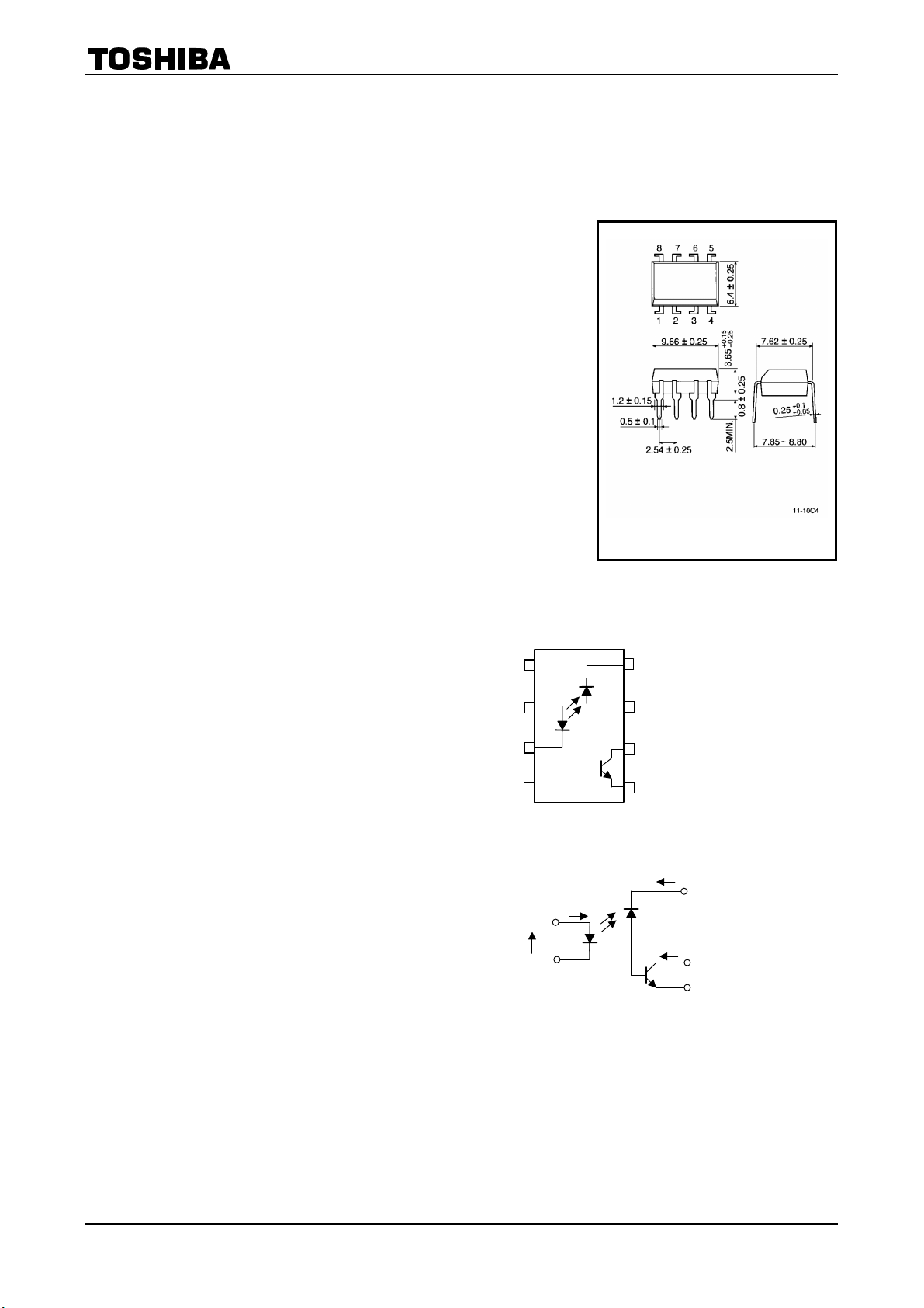
Pin Configuration
TOSHIBA 11−10C4
Weight: 0.54 g (typ.)
(top view)
TLP550
Unit in mm
1
2
3
4
8
7
6
5
1 : N.C.
2 : Anode
3 : Cathode
4 : N.C.
5 : Emitter
6 : Collector
7 : N.C.
8 : Cathode
Schematic
I
CC
V
I
F
2
V
F
3
CC
8
I
O
V
O
6
GND
5
2007-10-01 1

TLP550
Current Transfer Ratio
Current Transfer Ratio (%)
Classification
(IC/IF)
Marking of Classification
MIN MAX
(None) 10 ― Blank, O, Y
Rank O 19 ― O
Rank Y 35 ― Y
Absolute Maximum Ratings
(Ta = 25°C)
Characteristic Symbol Rating Unit
Forward current (Note 1) I
Pulse forward current (Note 2) I
Peak transient forward
current (Note 3)
LED
Reverse voltage V
Diode power dissipation
(Note 4)
Output current I
Peak output current I
Supply voltage V
Output voltage V
Detector
Output power dissipation
(Note 5)
Operating temperature range T
Storage temperature range T
Lead solder temperature (10s) T
Isolation voltage
(AC, 1min., R.H. = 40~60%) (Note 6)
I
FPT
P
OP
P
BV
FP
CC
opr
stg
sol
F
R
D
O
O
O
S
25 mA
50 mA
1 A
5 V
45 mW
8 mA
16 mA
−0.5~15 V
−0.5~15 V
100 mW
−55~100 °C
−55~125 °C
260 °C
2500 Vrms
Note: Using continuously under heavy loads (e.g. the application of high temperature/current/voltage and the
significant change in temperature, etc.) may cause this product to decrease in the reliability significantly even
if the operating conditions (i.e. operating temperature/current/voltage, etc.) are within the absolute maximum
ratings.
Please design the appropriate reliability upon reviewing the Toshiba Semiconductor Reliability Handbook
(“Handling Precautions”/
“Derating Concept and Methods”) and individual reliability data (i.e. reliability test report
and estimated failure rate, etc).
(Note 1) Derate 0.8mA above 70°C.
(Note 2) 50% duty cycle, 1ms pulse width.
Derate 1.6mA / °C above 70°C.
(Note 3) Pulse width 1μs, 300pps.
(Note 4) Derate 0.9mW / °C above 70°C.
(Note 5) Derate 2mW / °C above 70°C.
2007-10-01 2

TLP550
)
)
Electrical Characteristics
Characteristic Symbol Test condition Min. Typ. Max. Unit
Forward voltage V
Forward voltage
temperature coefficient
LED
Reverse current I
Capacitance between
terminal
High level output
current
Detector
High level supply
voltage
Current transfer ratio IO / I
Low level output
Coupled
voltage
Isolation resistance R
Capacitance between
input to output
Switching Characteristics
(Ta = 25°C)
F
/ΔTa IF = 16 mA ― −2 ― mV / °C
ΔV
F
R
C
T
I
OH (1)
I
OH (2)
I
OH
I
CCH
V
OL
S
C
S
(Ta = 25°C)
IF = 16 mA 1.45 1.65 1.85 V
VR = 5 V ― ― 10 μA
VF = 0, f = 1MHz ― 60 ― pF
IF = 0 mA, VCC = VO = 5.5 V ― 3 500 nA
IF = 0 mA, VCC = VO = 15 V ― ― 5 μA
IF = 0 mA, VCC = VO = 15 V
Ta = 70°C
IF = 0 mA, VCC = 15 V ― 0.01 1 μA
Ta = 25°C 10 30 ―
Rank : 0 19 30 ―
Rank : Y 35 50
Ta = 0~70°C 5 ― ―
F
IF = 16 mA
= 4.5 V
V
CC
= 0.4 V
V
O
Rank : 0, Y 15 ― ―
IF = 16 mA, VCC = 4.5 V
= 1.1 mA
I
O
(rank 0: I
R.H. = 40~60%, V = 1kV DC
(Note 6)
= 2.4mA)
O
V = 0, f = 1MHz ― 0.8 ― pF
― ― 50 μA
%
― ― 0.4 V
12
― 10
― Ω
Characteristic Symbol Test Condition Min. Typ. Max. Unit
Propagation delay time
(H→ L)
t
pHL
IF = 0→ 16 mA, VCC = 5V, RL = 4.1 kΩ ― 0.3 0.8
(Note 7) Rank 0: RL = 1.9 kΩ ― 0.5 0.8
Propagation delay time
(L→ H)
Common mode transient
immunity at high output
level
Common mode transient
immunity at low output
level
t
C
C
pLH
MH
ML
IF = 16→ 0 mA, VCC = 5V, RL = 4.1 kΩ ― 1.0 2.0
(Note 7) Rank 0: R
IF = 0 mA, VCM = 200 V
RL = 4.1 kΩ (rank 0: RL = 1.9 kΩ)
p−p
= 1.9 kΩ ― 0.6 1.2
L
― 1500 ― V /μs
(Note 8
IF = 16 mA, VCM = 200 V
RL = 4.1 kΩ (rank 0: RL = 1.9 kΩ)
p−p
― −1500 ― V /μs
(Note 8
(Note 6) Device considered two−terminal device: Pins 1, 2, 3 and 4 shorted together and pin 5, 6, 7 and 8 shorted together.
μs
μs
2007-10-01 3
 Loading...