

现货库存、技术资料、百科信息、热点资讯,精彩尽在鼎好!
TOSHIBA Photocoupler GaAs Ired & Photo-Thyristor
TLP541G,TLP542G
TLP541G, TLP542G
Programmable Controllers
AC−Output Module
Solid State Relay
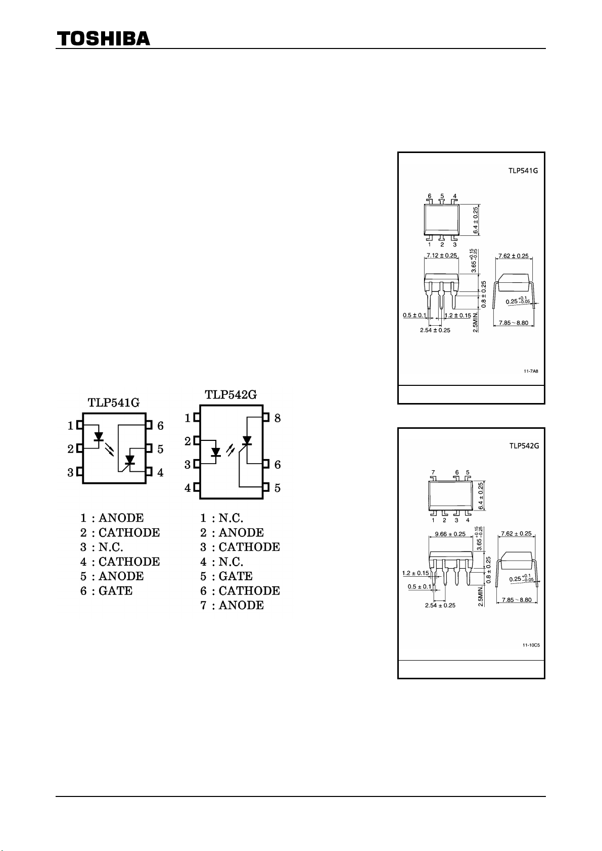
The TOSHIBA TLP541G consists of a photo−thyristor optically coupled
to a gallium arsenide infrared emitting diode in a six lead plastic DIP
package.
The TOSHIBA TLP542G consists of a photo−thyristor optically coupled
to a gallium arsenide infrared emitting diode in a seven lead plastic DIP
package.
• Peak off-state voltage: 400 V (min.)
• Trigger LED current: 7 mA (max.)
• On-state current: 150 mA (max.)
• Isolation voltage: 2500 V
• UL recognized: UL1577, file no. E67349
Pin Configuration
(min.)
rms
(top view)
Unit in mm
TOSHIBA 11−7A8
Weight: 0.4 g
TOSHIBA 11−10C5
Weight: 0.53 g
1
2002-09-25
TLP541G, TLP542G
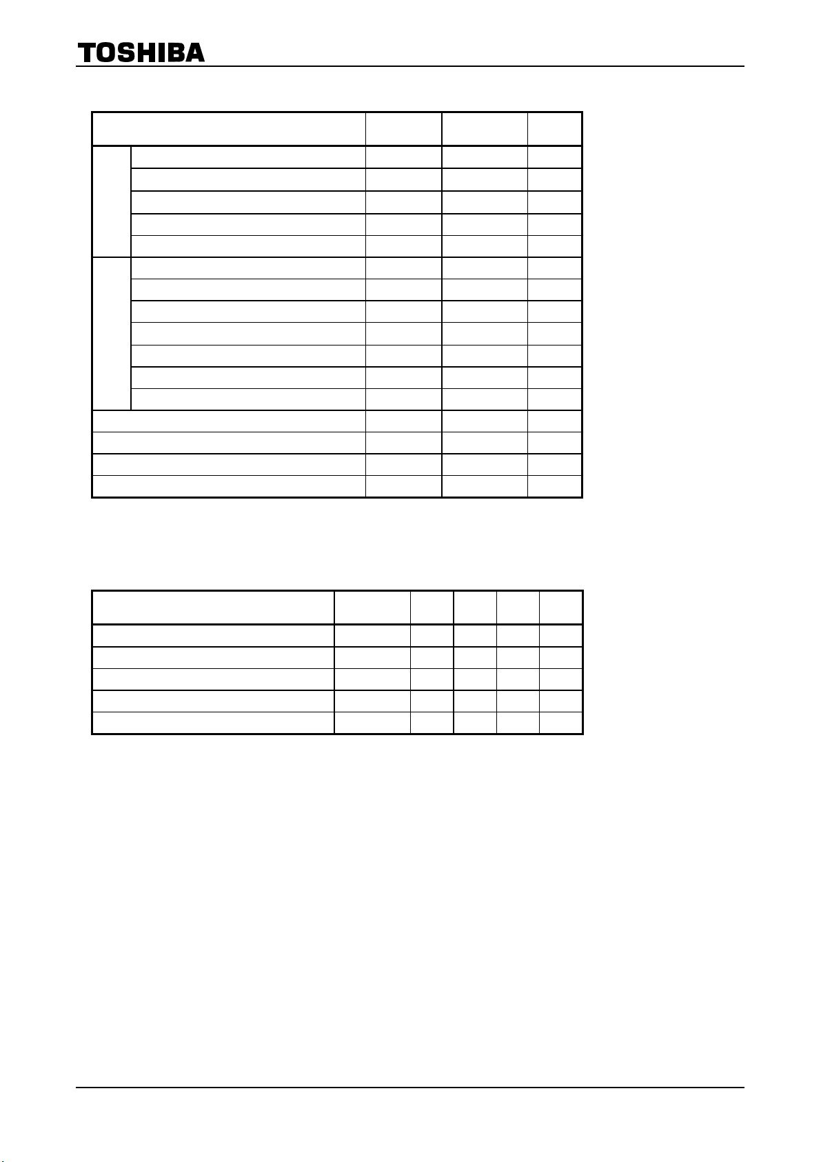
Maximum Ratings
Forward current IF 70 mA
Forward current derating (Ta ≥ 25°C) ΔIF / °C −0.7 mA / °C
Peak forward current (100 μs pulse, 100 pps) IFP 1 A
LED
Reverse voltage VR 5 V
Junction temperature Tj 125 °C
Peak forward voltage (RGK = 27kΩ) V
Peak reverse voltage (RGK = 27kΩ) V
On−state current I
On−state current derating (Ta ≥ 25°C) ΔIT / °C −2.0 mA / °C
Detector
Peak one cycle surge current I
Peak reverse gate voltage VGM −5 V
Junction temperature Tj 100 °C
Storage temperature range T
Operating temperature range T
Lead soldering temperature (10 s) T
Isolation voltage (AC, 1 min., R.H. ≤ 60%) (Note) BVS 2500 V
(Ta = 25°C)
Characteristic Symbol Rating Unit
400 V
DRM
400 V
RRM
150 mA
T (RMS)
2 A
TSM
−55~125 °C
stg
−30~100 °C
opr
260 °C
sol
rms
(Note) Device considered a two terminal device: LED side pins shorted together and detector side pins shorted
together.
Recommended Operating Conditions
Characteristic Symbol Min. Typ. Max. Unit
Supply voltage VAC ― ― 120 V
Forward current IF 10 16 25 mA
Operating temperature T
Gate to cathode resistance RGK ― 27 33 kΩ
Gate to cathode capacity CGK ― 0.01 0.1 μF
−30
opr
― 85 °C
ac
2
2002-09-25

TLP541G, TLP542G
Individual Electrical Characteristics
Characteristic Symbol Test Condition Min. Typ. Max. Unit
Forward voltage VF IF = 10 mA 1.0 1.15 1.3 V
Reverse current IR VR = 5 V ― ― 10 μA
LED
Capacitance CT V = 0, f = 1 MHz ― 30 ― pF
Off−state current I
Reverse current I
On−state voltage VTM ITM = 100 mA ― 0.9 1.3 V
Detector
Holding current IH RGK = 27 kΩ ― 0.2 1 mA
Off−state dv/dt dv/dt VAK = 280 V, RGK = 27 kΩ 5 10 ― V/μs
Capacitance Cj
Coupled Characteristics
Characteristic Symbol Test Condition Min. Typ. Max. Unit
(Ta = 25°C)
DRM
RRM
(Ta = 25°C)
V
AK
R
GK
V
KA
R
GK
V = 0, f = 1 MHz Anode to gate
Gate to cathode― ―
= 400 V
= 27 kΩ
= 400 V
= 27 kΩ
Ta = 25°C ― 10 5000 nA
Ta = 100°C ― 1 100 μA
Ta = 25°C ― 10 5000 nA
Ta = 100°C ― 1 100 μA
20
350 ― ―
pF
Trigger LED current IFT VAK = 6 V, RGK = 27 kΩ 1 4 7 mA
Turn−on time ton IF = 50 mA, RGK = 27 kΩ ― 10 ― μs
Capacitance
(input to output)
Isolation resistance RS VS = 500 V, R.H. ≤ 60% ― 1011 ― Ω
Isolation voltage BVS AC, 1 minute 2500 ― ― V
VS = 0, f = 1 MHz ― 0.8 ― pF
C
S
rms
3
2002-09-25

TLP541G, TLP542G
4
2002-09-25

TLP541G, TLP542G
5
2002-09-25

TLP541G, TLP542G
RESTRICTIONS ON PRODUCT USE
• The information contained herein is subject to change without notice.
• TOSHIBA is continually working to improve the quality and reliability of its products. Nevertheless, semiconductor
devices in general can malfunction or fail due to their inherent electrical sensitivity and vulnerability to physical
stress. It is the responsibility of the buyer, when utilizing TOSHIBA products, to comply with the standards of
safety in making a safe design for the entire system, and to avoid situations in which a malfunction or failure of
such TOSHIBA products could cause loss of human life, bodily injury or damage to property.
In developing your designs, please ensure that TOSHIBA products are used within specified operating ranges as
set forth in the most recent TOSHIBA products specifications. Also, please keep in mind the precautions and
conditions set forth in the “Handling Guide for Semiconductor Devices,” or “TOSHIBA Semiconductor Reliability
Handbook” etc.
• The TOSHIBA products listed in this document are intended for usage in general electronics applications
(computer, personal equipment, office equipment, measuring equipment, industrial robotics, domestic appliances,
etc.).These TOSHIBA products are neither intended nor warranted for usage in equipment that requires
extraordinarily high quality and/or reliability or a malfunction or failure of which may cause loss of human life or
bodily injury (“Unintended Usage”). Unintended Usage include atomic energy control instruments, airplane or
spaceship instruments, transportation instruments, traffic signal instruments, combustion control instruments,
medical instruments, all types of safety devices, etc.. Unintended Usage of TOSHIBA products listed in his
document shall be made at the customer’s own risk.
• The products described in this document shall not be used or embedded to any downstream products of which
manufacture, use and/or sale are prohibited under any applicable laws and regulations.
• The information contained herein is presented only as a guide for the applications of our products. No
responsibility is assumed by TOSHIBA for any infringements of patents or other rights of the third parties which
may result from its use. No license is granted by implication or otherwise under any patents or other rights of
TOSHIBA or the third parties.
20070701-EN
• GaAs(Gallium Arsenide) is used in this product. The dust or vapor is harmful to the human body. Do not break,
cut, crush or dissolve chemically.
• Please contact your sales representative for product-by-product details in this document regarding RoHS
compatibility. Please use these products in this document in compliance with all applicable laws and regulations
that regulate the inclusion or use of controlled substances. Toshiba assumes no liability for damage or losses
occurring as a result of noncompliance with applicable laws and regulations.
6
2002-09-25
 Loading...