

现货库存、技术资料、百科信息、热点资讯,精彩尽在鼎好!
TOSHIBA Photocoupler GaAs IRed & Photo−Transistor
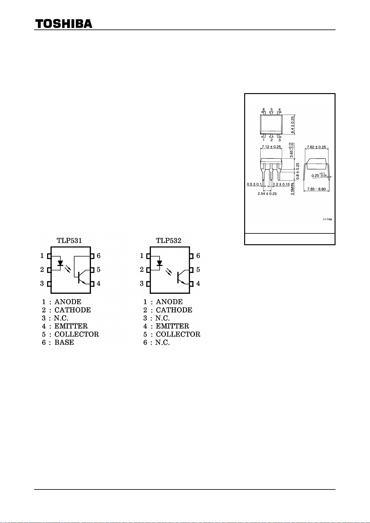
TLP531,TLP532
TLP531,TLP532
Programmable Controllers
AC / DC−Input Module
Solid State Relay
The TOSHIBA TLP531 and TLP532 consist of a photo−transistor
optically coupled to a gallium arsenide infrared emitting diode in a six
lead plastic DIP.
TLP532 is no−base internal connection for high−EMI environments.
· Collector−emitter voltage: 55 V (min.)
· Current transfer ratio: 50% (min.)
Rank GB: 100% (min.)
· Isolation voltage: 2500 V
· UL recognized: UL1577, file no. E67349
Pin Configurations
(min.)
rms
(top view)
Unit in mm
TOSHIBA 11−7A8
Weight: 0.4g
1
2002-09-25
TLP531,TLP532
Maximum Ratings
Forward current IF 70 mA
Forward current derating (Ta ≥ 50°C) ∆IF / °C 0.93 mA / °C
Peak forward current (100 µs pulse, 100pps) IFP 1 A
LED
Reverse voltage VR 5 V
Junction temperature Tj 125 °C
Collector-emitter voltage V
Collector-base voltage (TLP531) V
Emitter-collector voltage V
Emitter-base voltage (TLP531) V
Collector current IC 50 mA
Detector
Power dissipation PC 150 mW
Power dissipation derating (Ta ≥ 25°C) ∆PC / °C -1.5 mW / °C
Junction temperature Tj 125 °C
Storage temperature range T
Operating temperature range T
Lead soldering temperature (10s) T
Total package power dissipation PT 250 mW
Total package power dissipation derating (Ta ≥ 25°C) ∆PT / °C -2.5 mW / °C
Isolation voltage (AC, 1min., R.H.≤ 60%) BVS 2500 V
(Ta = 25°C)
Characteristic Symbol Rating Unit
55 V
CEO
80 V
CBO
7 V
ECO
7 V
EBO
-55~125 °C
stg
-55~100 °C
opr
260 °C
sol
rms
Recommends Operating Conditions
Characteristic Symbol Min. Typ. Max. Unit
Supply voltage VCC ― 5 24 V
Forward current IF ― 16 25 mA
Collector current IC ― 1 10 mA
Operating temperature T
-25 ― 85 °C
opr
2
2002-09-25
TLP531,TLP532
Individual Electrical Characteristics
Characteristic Symbol Test Condition Min. Typ. Max. Unit
Forward voltage VF IF = 10mA 1.0 1.15 1.3 V
Reverse current IR V
LED
Capacitance CT V = 0, f = 1MHz ― 30 ― pF
Collector-emitter
breakdown voltage
Emitter-collector
breakdown voltage
Collector-base
breakdown voltage (TLP531)
Emitter-base
Detector
breakdown voltage (TLP531)
Collector dark current I
Capacitance (collector to emitter) CCE V = 0, f = 1MHz ― 10 ― pF
V
(BR) CEOIC
V
(BR) ECOIE
V
(BR) CBOIC
V
(BR) EBOIE
CEO
Coupled Electrical Characteristics
Characteristic Symbol Test Condition Min. Typ. Max. Unit
(Ta = 25°C)
R
VCE = 24V ― 10 100 nA
V
CE
(Ta = 25°C)
= 5V ― ― 10 µA
= 0.5mA 55 ― ― V
= 0.1mA 7 ― ― V
= 0.1mA 80 ― ― V
= 0.1mA 7 ― ― V
= 24V, Ta = 85°C ― 2 50 µA
Current transfer ratio IC / IF
Collector-emitter
saturation voltage
V
CE (sat)
= 5mA, VCE = 5V
I
F
Rank Y
Rank YG
Rank GR
Rank GB
Rank BL
IC = 2.4mA, IF = 8mA ― ― 0.4 V
50 200 600
50 ― 150
50 ― 300
100 ― 300
100 ― 600
200 ― 600
%
3
2002-09-25

TLP531,TLP532
Isolation Characteristics
Characteristic Symbol Test Condition Min. Typ. Max. Unit
Capacitance
(input to output)
Isolation resistance RS VS = 500V, R.H.≤ 60% 5 ´ 1010 1014 ― Ω
Isolation voltage BVS AC, 1 minute 2500 ― ― V
(Ta = 25°C)
C
VS = 0, f = 1MHz ― 0.8 ― pF
S
Switching Characteristics
Characteristic Symbol Test Condition Min. Typ. Max. Unit
Rise time t
Fall time t
Turn-on time t
Turn-off time t
Turn-on time t
Storage time t
Turn-off time t
Turn-on time t
Storage time t
Turn-off time t
(Ta = 25°C)
r
f
ON
OFF
ON
s
OFF
ON
s
OFF
VCC = 10V
I
= 2mA
C
R
= 100Ω
L
RL = 1.9kΩ (Fig.1)
R
= open
BE
V
= 5V, IF = 16mA
CC
RL = 1.9Ω (Fig.1)
R
= 220kΩ (TLP531)
BE
V
= 5V, IF = 16mA
CC
― 2 ―
― 3 ―
― 3 ―
― 3 ―
― 2 ―
― 15 ―
― 25 ―
― 2 ―
― 12 ―
― 20 ―
rms
µs
µs
µs
Fig. 1 Switching time test circui
4
2002-09-25

TLP531,TLP532
5
2002-09-25

TLP531,TLP532
6
2002-09-25

TLP531,TLP532
7
2002-09-25

TLP531,TLP532
8
2002-09-25

TLP531,TLP532
A
RESTRICTIONS ON PRODUCT USE
· TOSHIBA is continually working to improve the quality and reliability of its products. Nevertheless, semiconductor
devices in general can malfunction or fail due to their inherent electrical sensitivity and vulnerability to physical
stress. It is the responsibility of the buyer, when utilizing TOSHIBA products, to comply with the standards of
safety in making a safe design for the entire system, and to avoid situations in which a malfunction or failure of
such TOSHIBA products could cause loss of human life, bodily injury or damage to property.
In developing your designs, please ensure that TOSHIBA products are used within specified operating ranges as
set forth in the most recent TOSHIBA products specifications. Also, please keep in mind the precautions and
conditions set forth in the “Handling Guide for Semiconductor Devices,” or “TOSHIBA Semiconductor Reliability
Handbook” etc..
· The TOSHIBA products listed in this document are intended for usage in general electronics applications
(computer, personal equipment, office equipment, measuring equipment, industrial robotics, domestic appliances,
etc.). These TOSHIBA products are neither intended nor warranted for usage in equipment that requires
extraordinarily high quality and/or reliability or a malfunction or failure of which may cause loss of human life or
bodily injury (“Unintended Usage”). Unintended Usage include atomic energy control instruments, airplane or
spaceship instruments, transportation instruments, traffic signal instruments, combustion control instruments,
medical instruments, all types of safety devices, etc.. Unintended Usage of TOSHIBA products listed in this
document shall be made at the customer’s own risk.
· The information contained herein is presented only as a guide for the applications of our products. No
responsibility is assumed by TOSHIBA CORPORATION for any infringements of intellectual property or other
rights of the third parties which may result from its use. No license is granted by implication or otherwise under
any intellectual property or other rights of TOSHIBA CORPORATION or others.
· The information contained herein is subject to change without notice.
000707EA
9
2002-09-25
 Loading...