

Page 1

FILE NO. 336-9707
TECHNICAL TRAINING MANUAL
3 LCD D ATA PROJECTOR
TLP511U
TLP510U
TLP511E
TLP510E
PRINTED IN JAPAN, Nov., 1997
S
Page 2

CONTENTS
1. MAIN POWER SUPPLY
CIRCUIT .....................................1-1
1-1. Description .................................................1-1
1-2. Output Control ..........................................1-1
1-3. Voltage Switching ...................................... 1-1
1-4. Over-voltage Protection............................ 1-1
1-5. Over-current Protection ........................... 1-2
1-6. Overheat Protection ..................................1-2
2. LAMP POWER SUPPLY
CIRCUIT (LAMP DRIVER).....2-1
2-1. Configuration.............................................2-1
3. OPTICAL SYSTEM...................3 -1
3-1. Configuration.............................................3-1
4. R.G.B. DRIVE CIRCUIT...........4-1
4-1. Outline ........................................................ 4-1
4-2. Operation Description .............................. 4-3
5. MICROPROCESSOR................5-1
5-1. System Outline...........................................5-1
5-2. System Microprocessor.............................5-3
5-3. Power Supply Reset Process..................... 5-4
5-4. Non-volatile Memory Process ..................5-4
5-5. Remote Control Reception Process..........5-4
5-6. RS-232C T ransmission/
Reception Process...................................... 5-4
5-7. Status Read Process .................................. 5-4
5-8. Status Display Process ..............................5-5
5-9. On-screen Display Process........................ 5-5
5-10. Video System Control Process.................. 5-6
5-11. Panel System Control Process.................. 5-6
5-12. Drive System Control Process.................. 5-7
5-13. Various Display Modes .............................5-7
5-14. Applicable Signal.......................................5-8
5-15. RS-232C Control Method ......................... 5-9
6. DIGITAL CIRCUIT ...................6-1
6-1. Outline ........................................................ 6-1
6-2. Each IC Description ..................................6-3
7. VIDEO SIGNAL PROCESS
CIRCUIT .....................................7-1
7-1. Circuit Component.................................... 7-1
7-2. Input Signal Switch Section...................... 7-3
7-3. Video Demodulation Block....................... 7-5
7-4. RGB Signal Amplification Section.........7-12
7-5. Microprocessor Interface .......................7-14
8. CCD CAMERA CIRCUIT
(For TLP511)...............................8 -1
8-1. Outline ........................................................ 8-1
9. FLUORESCENT LAMP
INVERTER CIRCUIT
(For TLP511)...............................9 -1
9-1. Operation Description .............................. 9-1
9-2. Troubleshooting .........................................9-2
9-3. Circuit Diagram......................................... 9-3
i
Page 3

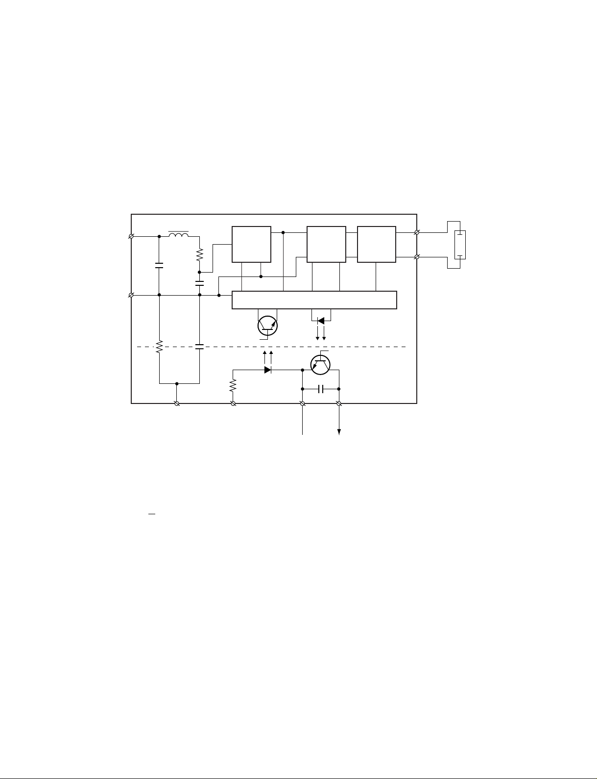
1. MAIN POWER SUPPLY CIRCUIT
1-3. Voltage Switching
1-1. Description
This power supply boosts up at boost-up-converter just
after bridge-rectifying AC input voltage, supplies the
voltage smoothed to DC 350V to the lamp output. Then
current resonance DC-DC converter which uses the DC
350V as an input converts the voltage and supplies S6V,
+6V, +10V, +13V, +15.5V and –12V.
The boost-up-converter control IC, IC301, stabilizes AC
rectified voltage to DC 350V. The current resonance DCDC converter, IC303, turns FET Q102 and Q103 “ON/
OFF” alternately using the drive transformer T103 and
converts the voltage to secondary side through the
converter transformer T101. At this time, the voltage of
S6V at the secondary side is detected by IC402, the
negative feedback to IC303 is carried out at photo
coupler PH301 and then the voltage is stabilized. Other
outputs are determined by the turn ratio of secondary
side of T101, and the voltage rectified, smoothed, but not
stabilized are stabilized through the series regulator.
(+10V is stabilized at IC203, +13V at IC202, +15.5V at
IC201.)
The voltage rectified and smoothed by D105 and C113 at
primary winding of T101 is supplied as a VCC voltage of
IC301, IC302 and IC303 on primary side ICs, and also
the voltage rectified and smoothed by D106 and C114 is
supplied as a gate bias voltage of D306 TRIAC (triode
AC switch) which short-circuits the inrush current
limiting resistor R305. Therefore, when the electric
current resonance DC-DC converter stops to oscillate, the
VCC voltage is not supplied so that the boost-upconverter stops to operate.
1-2. Output Control
When the voltage switching terminal of connector C
opens, pin 1 develops low, since the pin 2 of IC401 is 6V,
higher than pin 2 (3V), the voltage adjusted to 16.3V is
directly developed from IC201, since the status of Q205
turns off. When the voltage switching terminal develops
ground potential, since pin 2 of IC401 develops 0V and
the voltage of pin 2 develops low, pin 1 develops high,
Q205 turns on, voltage-set-up resistor of R201 is shortcircuited and the voltage of IC201 rises from 16.3V to
18.0V.
1-4. Over-voltage Pr otection
When the negative feedback circuit of current resonance
DC-DC converter is shut down, the secondary side
voltage control is unable to operate, the voltage begins to
develop high without any restriction. At this time, when
the voltage of S6V and +6V exceeds 8.5V, the base of
transistor Q401 is biased through the zener diode D201,
and turns on, and then the voltage higher than 7V is
added to pin 6 (OVP) of IC303 through the photo coupler
PH302. When the voltage higher than 7V is added to pin
6, IC303 is latched, all outputs are shut down. ( Boostup-converter stops simultaneously, too.)
When the voltage is added to +10V, +13V, +15.5V lines
from external side, (exceeding +15V for +10V line, 13V
for +13 line and 20V for +15.5V line), on each line
respectively through the zener diodes D202, D203 and
D204, the base voltage of Q401 is biased passing, IC303
is latched in the same way as the above-mentioned, all
outputs are shut down. When releasing the latch operation, stop to supply the commercial power supply and
then re-supply the commercial power after more than
approx. 120 seconds.
When the output control 1 and 2 of connector A develops
low, the voltage of approx. 14V is added to Q203 gate
and pins 4 of IC203, IC201, and IC202 through R205
and R206 respectively, since the transistors Q201 and
Q202 turn off. In this case, Q204, IC201, IC202 and
IC203 turn off, the voltages of +6V, +10V, +15.5V and
+13V are not developed.
When the output control 1 and 2 develop high, the
transistors Q201 and Q202 turn on, so no voltage is
added to the gate Q203, IC201, IC202 and IC203,
described above, and the voltage of +6V, +10V, –15.5V
and +13V are developed.
1-1
Page 4

1-5. Over-curr ent Protection
In S6V and +6V lines, the voltage drop owing to the
current flowing in L203 is detected by pins 5 and 6 of
IC401, when the total current amount exceeds 8A, pin 7
develops high and the voltage biasses the base voltage of
transistor Q401 passing through the zener diode D402
and diode D401. In the same way as described in the
item of the over-voltage protection, IC303 is latched and
all outputs are shutdown. The method to release the latch
operation is the same as the item of the over-voltage
protection.
Over-current protection at +10V, +13V, +15.5V lines are
carried out by the over-current protection characteristic
provided with the series regulator ICs (IC203, IC202 and
IC201). Refer to Fig. 1-5-1.
In this case, as only the line short-circuiting or overloading is protected, no effect appears on other outputs. The
protection is released by removing the over current
flowing condition.
When short-circuiting or overloading continues, the IC
overheats and the overheat protection circuit inside the
IC works to shut down the output voltage. In this case,
the overheat protection is released by unloading the
current and removing the overheat of IC.
100
80
60
40
20
Relative output voltage (%)
0
0 1.0 2.0 3.0 4.0
Output current Io (A)
Fig. 1-5-1
<Supplement>
The over-current protection for lamp output detects the
voltage drop of the current detection resistor R113 at
between pins 9 and 10 of IC302. When voltage switching
terminal of connector C opens (at 16.3V), the photo
coupler PH303 turns off since pin 1 of IC401 develops
low and the voltage of drop voltage at R113 is directly
compared at pin 10 of IC302. When the lamp output
current is from 0.7 to 0.9A, pin 8 develops high and the
voltage higher than 7V is added to pin 6 of IC303. Then
IC303 is latched and all outputs are shut down.
When the voltage switching terminal of connector C
develops the ground potential (at 18.0V), pin 1 of IC401
develops high, PH303 turns on and the voltage of drop
voltage at R113 and the voltage divided by R317 and
R327 are compared at pin 10 of IC302. When the lamp
output is from 1.05 to 1.35A, pin 8 of IC302 develops
high, IC303 is latched and all outputs are shut down. The
method to release the latch operation is the same as the
over-voltage protection description.
1-6. Overheat Protection
As an overheat protection of the power supply, the
temperature of switching FET Q301 of the boost-upconverter is detected. Positive characteristic thermistor
TH301 for temperature detection is attached on the heat
sink of Q301. When Q301 is overheated owing to the
overload and/or defect of cooling fan, etc., the resistor
value of TH301 increases abruptly, while the surface
temperature exceeds approx. 120°C. Then the transistor
Q302 turns on, the voltage higher than 7V is added to the
pin 6 (OVP) of IC303, IC303 is latched and all outputs
are shut down.
When releasing the latch operation, stop to supply the
commercial power by canceling, cool enough after more
than approx. 120 seconds, and then re-supply the
commercial power.
1-2
Page 5
2. LAMP POWER SUPPLY CIRCUIT
(LAMP DRIVER)
2-1. Configuration
The lamp power supply cicrcuit receives a DC220 to
390V (primary side) from the system power supply and
provides a AC voltage (70 to 100VAC at ever turning on
the lamp) to turn on the lamp. Fig. 2-1-1 shows the block
diagram.
Lamp Driver
L1
Stabilizer Igniter
R1
C1
Power
input
C2
CsRs
CB3
EMC GND
(optional)
I122
1K
CB2-1
SCI
The DC voltage is supplied to CB1 from the main power
supply unit through an interlock switch. This voltage
becomes AC input x 2Ö2 (= 340V for AC120V input)
when the lamp is off. CB2 is a connector for the lamp on
control signal input (SCI) and lamp off control signal
output (FLAG). When +5V is applied to SCI (CB2-1) in
the standby on, I122 FET transistor turns on, the igniter
develops a high voltage pulse (5 to 25 kV), and the lamp
starts to light up.
Commu-
tator
Control
100nF
CB2-2
Common Flag
Fig. 2-1-1
The pulse normally continues to be developed until the
lamp turns on (for max. 3s.). But if the lamp does not
turn on, I121 does not turn on, the voltage of CB2-3
develops high. I121 turns on and develops low after the
lamp turned on, the igniter circuit stops the operation.
Then the AC70 to 100V is applied to the lamp.
I121
L1
L2
Lamp
Mains
isolated
2-1
Page 6
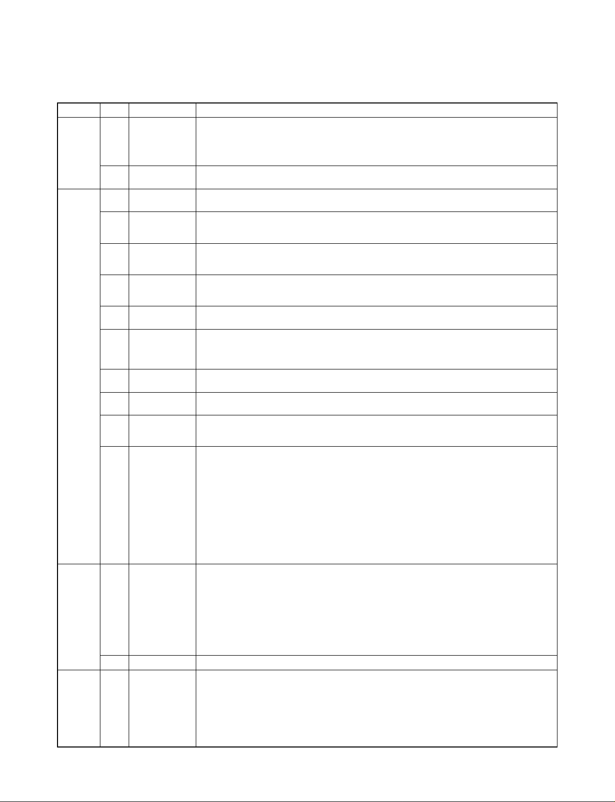
3. OPTICAL SYSTEM
3-1. Configuration
Lamp
unit
Mirror
box
unit
Prism
unit
Projection
lens
No.
1
2
3
4
5
6
7
8
9
10
11
12
13
14
15
Name
UHP lamp
Parabolic
reflector
UV IR filter
Multi-lenses
A, B
Polarization
light beam
splitter (PBS)
Phase
difference
plate
Condenser
lens
Dichroic
mirror
Full reflection
mirror
Field lens
Relay lens
Incident side
polarized
plate/Phase
difference
plate
Liquid crystal
panel
Cross prism
Projection
lens
Description
Light source of the optical system. AC lighting system 120W, arc length 1.3 mm.
As the arc length is shorter than the conventional metal halide lamp, the light source
operates as an ideal light point source and this improves the light convergence factor.
Also, the color temperature gets higher and this allows to reproduce more natural
white color.
Parabolic reflector converges light emitted from the UHP lamp forward in approximate
parallel light beams and illuminates the liquid crystal panel.
Optical filter to pass necessary visible rays and cut unnecessary ultraviolet rays and
infrared rays among light emitted from the UHP lamp.
Tw o multi-lenses A and B allow a circular beam light emitted from the light source to
illuminate the square liquid crystal panel evenly, thus providing projected pictures
with less brightness variation.
Separates the illuminating light from the light source into P polarization light and S
polarization light and leads both light to the multi-lens B with a little angle.
Converts the polarization direction of incident light via the multi-lens B into another
direction. Here, P polarization light waveform separated by PBS is converted into
another S polarization light waveform.
Converges the illuminating light emitted from the light source into the liquid crystal
panel.
Separates the white light emitted from the light source into RGB three primary colors.
The white light emitted from the light source reflects B light using a dichroic mirror 1
and the RG lights pass through the dichroic mirror 1. Of the RG lights passed, G light
is reflected by the dichroic mirror 2 and R light passes.
Reflection mirror to lead the R and B lights separated by the dichroic mirrors 1 and 2
to the liquid crystal panel.
Light transmitted through liquid crystal panel is converged in direction of focal point
and effectively entered entrance pupil of the projection lens.
In the R axis optical path which is longer than those of G, B, the relay lens works as
a correction lens to arrange the illumination distribution of the liquid crystal panel
surface with that of other liquid crystal panel.
The illumination lights separated into RGB have the S polarizing waveform component in processing the PBS and phase difference plate operation previously described.
The incident side polarized plate arranges the illumination light more effective direct
polarizing waveform. The phase difference plate used works to converge the S
polarizing waveform into the P polarizing waveform which fits to the transparent axis
of the liquid crystal panel.
Since the phase difference plate possesses the wavelength characteristics for light,
each RGB axis employs exclusive phase difference plate. These polarizing plates
and difference plates are constructed in one plate by attaching each other, and put
on a glass plate.
To increase the color pur ity ratio of three primar y colors, the glass plate possess the
dichroic filter characteristics for RG axis.
Light exit side polarized plate is put on the light exit plane. When no signal voltage is
applied, the polarization direction of transmission light rotates by 90 degrees. When a
voltage is applied, the polarization direction is controlled owing to the voltage
applied. That is, the liquid crystal panel employs such general TN type liquid crystal.
In this model, the incidence/exit polarization plate is placed (in normally white mode)
so that the light transmission amount becomes maximum (white) when no voltage is
added and the light transmission amount becomes minimum (black) when maximum
voltage is added.
According to the liquid crystal panel specification, exclusive panel for each RGB axis
is employed and shown by identification seals.
Works to mix RGB lights passed through the liquid crystal panel.
Demodulated by the video signal on the liquid crystal panel and projects pictures
displayed on the liquid crystal at a screen. Light axis of the projection lens is set at
upper side of center of the liquid crystal panel and this realizes easy viewing of the
panel because the projected screen position is upper than the unit position. The
projected light shows S polarizing waveform and is compatible with the polarizing
screen.
The projection lens employs the zoom & focus system and allows to project enlarging
a picture upto maximum approx. 300 inch.
3-1
Page 7
15
XGA 1.3 inch 3 plates system
14
10
9
9
11
-2
13
-3
10
12
12
9
-1
13
13
10
8
8
-2
-1
7
6
1
UHP (120W)
2
3
4
A
5
4
B
Fig. 3-1-1 Optical configuration diagram
3-2
Page 8
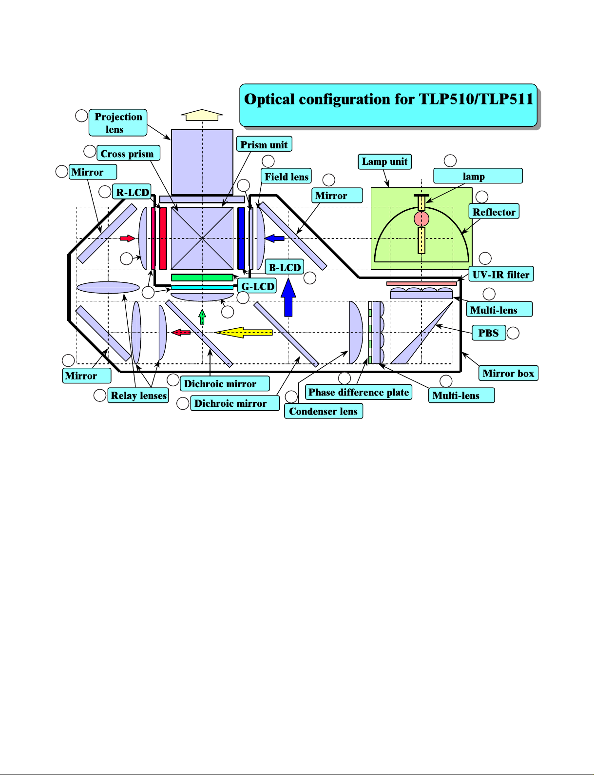
4. R.G.B. DRIVE CIRCUIT
1
1022 1023 1024
23
1st line
768 lines
768th line
1024 pixels
4-1. Outline
The outline of RGB drive circuit is described below
using the G process of the RGB drive circuit as an
example.
Odd number
pixel memory
Even number
pixel memory
Frame inverted
Digital PC board Drive PC board
SW2
SW1
1
DAC1 Amp.
2
1
DAC2
2
Q502
Q504
Amp.
Line inverted
Q505,Q506,Q507
Normal
amp.1
Q508,Q509,Q510
Inverted
amp.1
Q511,Q512,Q513
Normal
amp.2
Q523,Q524,Q510
Inverted
amp.2
1
2
1
2
Q514
SW3
Q514
SW4
Exclusive for odd number pixel
Q515
SW5
1
2
1
2
12-phase decomposite
Q516
&
Sample hold
1
Q515
SW6
even number pixel
&
Sample hold
2
Q517
Exclusive for
6-Phase decomposite
6-Phase decomposite
(12-phase collectively input)
Panel
VIDEO
input
12-phase composite
1
2
3
4
5
6
7
8
9
10
11
12
In the panel, 1024 pixels are arranged in a horizontal
direction and 768 lines of the pixels are in a vertical as
shown in Fig. 4-1-2.
As an H inverted drive system is employed, the panel
input signal waveform is as shown in Fig. 4-1-3.
Black level
White level
Center voltage
1st line
2nd line
White level
Black level
1st frame 2nd frame
Fig. 4-1-3
1st line
2nd line
Fig. 4-1-1
Fig. 4-1-2
4-1
Page 9
The signal as shown in Fig. 4-1-1 is separated into the
odd and even pixels at the digital PC board. After the
signal process is carried out in the drive PC board, the
odd and even pixel signals are synthesized to
decomposite the signal on the panel.
Referring to Fig. 4-1-1, the operation principle is
described.
When assuming;
1) the signal passing through DAC1 ® Q502 ® Normal
amp. 1 ® SW31 ® SW5 ® Q516 to the positive
phase 1,
2) the signal passing through DAC1 ® Q502 ® inverted
amp. 1 ® SW32 ® SW5 ® Q516 to the inverted
phase 1,
<1st frame>
3) the signal passing through DAC2 ® Q504 ® Normal
amp. 1 ® SW41 ® SW6 ® Q517 to the positive
phase 2 and
4) the signal passing through DAC2 ® Q504 ® inverted
amp. 2 ® SW42 ® SW6 ® Q517 to inverted phase
2,
the AC and DC levels of the positive phases 1, 2 and the
inverted phases 1, 2 are expected to be the same.
However, each voltage will vary slightly owing to the
adjustment variation. In this case, each frame signal is
assumed as follows.
Center voltage
Normal phase 1
voltage
Normal phase 2
voltage
<2nd line>
Inverted phase 2
voltage
Inverted phase 1
voltage
Center voltage
Inverted phase
2 voltage
Inverted phase
1 voltage
12345 6 7 8 9 10 11 12 Pixel
1st line
1 2 3 4 5 6 7 8 9 10 11 12 Pixel
1st line
Normal phase 1
voltage
Normal phase 2
voltage
123
1 2 3 4 5 6 7 8 9 10 11 12 Pixel
456789101112 Pixel
2nd line
2nd line
As shown in Fig. 4-1-4, even if a slight level difference
occurs among the positive phases 1, 2 and inverted
phases 1, 2 signals (approx. 100 mV), the level difference will be decreased visually by reducing the level
Fig. 4-1-4
variation of the same line between each frame and
inverting the pixel voltage of the adjacent lines (1st line
and 2nd line) between each frame.
4-2
Page 10
4-2. Operation Description
The video signal of the odd number pixel (even number
pixel) is sent to Q501 (Q503) base and supplied to pin 16
of Q502 (Q504), LM1201M. The signal is clamped at
pin 16 and the pedestal voltage is adjusted at pin 6 after
the DC level is stabilized and then AC level is adjusted at
pin 3.
The signal is developed from pin 8, supplied to the buffer
circuits of Q505 – Q507 and Q511 – Q513, and supplied
to the inverted circuits of Q508, Q509, Q510, Q523,
Q525 and Q510. These signals are supplied to pins 5, 6,
8, 13, 15 and 16 of 12 phases development IC.
CXA2504N, Q516 and Q517 of sample-and-hold passing
through the SW circuit composed of Q514 and Q515.
The signals are developed from pins 37, 35, 33, 25 and
23 for each input.
The signals at pins 4, 7, 14 are used as bias input and the
bias inputs set the center DC voltage of output equal to
the bias voltage.
Q519 works to suppress the noise occurred at 12 phases
collective input process of the panel.
4-2-1. Outline of Liquid Crystal Panel
The liquid crystal panel module is an active matrix panel
with a built-in driver of multi-crystal silicon. The liquid
crystal panel module is designed for use of color projectors in combination with an enlargement projection
system and dichroic mirror.
<Basic specification>
(1) Screen size 26.624 (W) x 19.968 (H)
(2) Pixel number 1024 (W) x 768 (H)
(3) Applicable to XGA
(4) Monochrome panel
(5) Drive system H inverted drive
(6) Dot clock 65 MHz
(7) Inverted function for UP/DOWN/LEFT/RIGHT di-
rections
4-2-2. Basic Component
Pin No.
1
2
3
4
5
6
7
8
9
Name
DT
CLY
CLY
VDDY
NRS2
NRS1
LCCOM
VID11
VID9
Pin No.
10
11
12
13
14
15
16
17
18
Table 4-2-1 Terminal description
Name
VID7
VID5
VID3
VID1
VSSX
CLX
CLX
DX
VDDX
Pin No.
19
20
21
22
23
24
25
26
27
Name
DIRX
DIRX
ENB2
ENB1
VSSX
VID2
VID4
VID6
VID8
Pin No.
28
29
30
31
32
33
34
35
36
Name
VID10
VID12
LCCOM
N.C.
NRG
DY
DIRY
DIRY
VSSY
4-3
Page 11
Table 4-2-2 Input terminal function description
Name
DX
CLX, CLX
DIRX, DIRX
ENB1 – ENB2
VID1 – VID12
DY
CLY , CLY
DIRY, DIRY
LCCOM
VDDX
VDD Y
VSSX
VSSY
NRG
NRS1 – NRS2
Function
Start pulse input ter minal of X shift register composing X driver.
Transfer clock input terminal X shift register composing X driver
X driver driving direction switch input terminal (DIRX = H R shift, DIRX = L L shift)
X driver enable pulse input terminal
X driver video signal input terminal
Start pulse input ter minal of Y shift register composing Y dr iver.
Transfer clock input terminal of Y shift register composing Y driver.
Transfer clock input terminal of Y shift register composing Y driver. (DIRX = H Down shift,
DIRX = L Up shift)
Diagonal electrode potential input terminal of liquid crystal panel
X driver positive power supply input terminal
Y driver positive power supply input terminal
X driver negative power supply input terminal
Y driver negative power supply input terminal
Drive signal input terminal for auxiliary signal circuit
Auxiliary signal input terminal
4-4
Page 12

5. MICROPROCESSOR
5-1. System Outline
The system microprocessor has features as shown below.
In considering easy maintenance for specification
modification, etc., the program content is written in the
built-in non-volatile memory.
The program is also developed in considering use of
structured notation, parts modularity, and multi filling
system.
Major functions of the system microprocessor are as
follows.
5-1-1. System Control
• Microprocessor program write process
• Non-volatile memory control process
• Remote control reception process
• RS-232C transmission/reception process
• Status read process
• On-screen display process
5-1-3. Adjustment Control
• Video controls (high & low brightness ratio,
brightness, color density, tint, sharpness)
• Panel adjustments (V position, H position,
phase, clock, user registration, user read-out)
• Mode adjustments (Wide, MIC, OSD mute,
projection)
• Language adjustments (English, Japanese,
French, German, Spanish, Italian)
5-1-4. Adjustment Control at Factory Delivery
• Video sub adjustments (RGB gain, sub-bright)
• Drive adjustments (each item for panel controls,
RGB trimming)
Fig. 5-1-1 shows the system block diagram.
5-1-2. Normal Control
• Power ON/OFF
(Main/Fan/Lamp)
• Input switch (RGB/Video/Camera)
• Sound volume control UP/DOWN
• Menu
• Adjust (Up/Down/Left/Right)
• All mute ON/OFF
• Audio mute ON/OFF
• Display ON/OFF
• Freeze ON/OFF
• Resize ON/OFF
• Focus UP/DOWN
(at camera use)
• Zoom UP/DOWN
(at camera use)
5-1
Page 13
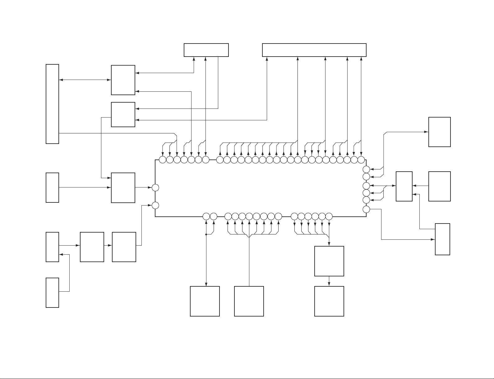
PL004PL010
5-2
PL001
2
/
3
/
PL006 QL003
PQ20VZ1U
PL001
HC125
QL012
HC125
QL005PL003
HC14
QL004
RN5VD27A
19
2
/
2
/
5
/
DRIVE
SENSOR
PL009
/
/
/
2
2
10117978457
77
QL002
HD64F3337YF16
1
16 17 24232221
25 26 27 28 44
12
/
/
4
4342414039
/
3
2
/
55596063646566676869707172747576
54
496162
58
57
53
52
51
48
6
/
2
QL010
HC165
3
/
PL002
/
2
CAT24C16J
QL006
/
8
SW LED
Fig. 5-1-1 System block diagram
HC541
6
/
QL007
Page 14
5-2. System Microprocessor
The system microprocessor QL002 employs an 8 bit
micro-controller (HD64F3337YF16).
In this system microprocessor, a program area is provided inside the non-volatile memory.
Table 5-2-1 Terminal functions of the system microprocessor
Using an exclusive data-writer allows easy maintenance
of the system microprocessor when specification modification, bug correction, etc. will occur.
Table 5-2-1 shows the terminal functions of the system
microprocessor.
Pin No.
1
2
3
4
5
6
7
8
9
10
11
12
13
14
15
16
17
18
19
20
21
22
23
24
25
26
27
28
29
30
31
32
33
34
35
36
37
38
39
40
Name
RES
XTAL
EXTAL
MD1
MD0
NMI
FVPF
VCC1
WDT
RXD0
TXD0
GND1
SDA
f
SEL
EEPCK
EEPDT
VD
REMOCON
AUX
KEY0
KEY1
KEY2
KEY3
KEY4
KEY5
KEY6
KEY7
AVCC
AD0
AD1
AD2
AD3
AD4
AD5
AD6
AD7
AGND
LED0
LED1
Function
Reset input
Clock input for oscillation
Clock output for oscillation
Mode 1
Mode 2
Priority interruption
Memory write voltage
Digital power supply
Not used
RS-232C reception for camera
RS-232C transfer for camera
Digital ground
Not used
Oscillation clock
Remote controller selection
Non-volatile memory clock
Non-volatile memory data
Not used
Remote controller reception
Not used
Key input 0
Key input 1
Key input 2
Key input 3
Key input 4
Key input 5
Key input 6
Key input 7
Analog power supply
Not used
Not used
Not used
Not used
Not used
Not used
Not used
Not used
Analog ground
LED data 0
LED data 1
I/O
O
O
O
I/O
O
O
O
I/O
O
O
O
Pin No.
I
I
I
I
I
I
I
I
I
I
I
I
I
I
I
I
I
I
I
I
I
I
I
I
I
I
I
I
I
41
42
43
44
45
46
47
48
49
50
51
52
53
54
55
56
57
58
59
60
61
62
63
64
65
66
67
68
69
70
71
72
73
74
75
76
77
78
79
80
Name
LED2
LED3
LED4
LED5
MAIN. PW
FAN. PW
V
CC2
LAMP. PW
OSDL
DDCV
SENL
SENC
SEND
VD0C
VD0D
GND2
DRVC
DRVD
OSDC
OSDD
PLLU
SYGL
SYGC
SYGD
D0
D1
D2
D3
D4
D5
D6
D7
GND3
CLK
R/W
ENB
RST
TXD1
RXD1
SCL
Function
LED data 2
LED data 3
LED data 4
LED data 5
Main power supply swtich
Fan power supply switch
Digital power supply
Lamp power supply switch
OSD load
Not used
Sensor load
Used for sensor
Used for sensor
Video I2C clock
Video I2C data
Digital ground
Drive I2C clock
Drive I2C data
OSD clock
OSD data
PLL enable
SYG load
SYG clock
SYG data
T-FORC data 0
T-FORC data 1
T-FORC data 2
T-FORC data 3
T-FORC data 4
T-FORC data 5
T-FORC data 6
T-FORC data 7
Digital ground
T-FORC clock
T-FORC read/write
T-FORC enable
T-FORC reset
RS-232C transfer for control
RS-232C reception for control
Not used
I/O
O
O
O
O
O
O
I
O
O
I
O
O
I
O
I/O
I
O
O
O
O
O
O
O
I/O
O
O
O
O
O
O
O
O
I
O
O
O
O
O
I
O
5-3
Page 15

5-3. Power Supply Reset Process
5-5. Remote Control Reception Process
In the power supply reset process, power supply reset IC
(RN5VD27A), QL004 is employed.
The reset IC,QL004, develops the reset signal when the
power supply voltage for the microprocessor varies and
becomes lower than the specified voltage, and sends the
signal to the reset terminal of the system microprocessor
(QL002).
5-4. Non-volatile Memory Control Process
In the non-volatile memory process, data reading and
saving for various adjustments are carried out on the
non-volatile memory, QL006 (CAT24C16J).
When the power (AC) is on, all the adjustment data are
read out by the system microprocessor (QL002), then the
previous status is realized.
When saving the data, all the adjustment data are written
by the system microprocessor (QL002), then the current
status is preserved.
However, if a failure (such as power interruption due to
lightning, etc.) occurs during the adjustment data writing,
a data error may occur. If the data is determined as
incorrect, the initial data memorized on the system
microprocessor (QL002) is read out and stored on the
non-volatile memory.
In the remote control reception process, a remote control
unit (CT-9925) connected to the remote control terminal
emits a remote control signal and a remote control signal
receive section on the front panel, the rear panel or the
camera arm (for TLP511) decodes the signal.
The remote control signals for rear panel and camera
section (for TLP511) are selected by QL012 buffer
(TC74HC125AF). Then both signals are mixed with the
remote control signal for front panel through QL005
buffer (74HC14AF).
Finally, the signal mixed is supplied to the remote control
terminal of the system microprocessor (QL002).
5-6. RS-232C Transmission/Reception
Process
In the RS-232C transmission/reception process, an RS232C signal entered through the RS-232C connector (DSUB 9P) is decoded in the RS-232C interface
(mPD4721), and fed to RXD1 terminal of the system
microprocessor (QL002).
In the RS-232C transmission process, RS-232C signal
developed from TXD0 terminal of the system microprocessor (QL002) is decoded in the RS-232C interface
(mPD4721) and fed to the camera microprocessor
section.
Signal name
Pin No.
QL010
(L)
(H)
A
11
FAN1. ER
Abnormal
Normal
5-7. Status Read Process
In the status read process, the following status shown in
the table below are read by QL010 (74HC165AF) and
the error process corresponding to each status is carried
out.
Table 5-7-1 shows the contents of the status read signals
and the logic.
Table 5-7-1 The contents of the status read signals and the logic
B
12
FAN1. SW
Normal
Abnormal
C
13
FAN2. ER
Abnormal
Normal
D
14
E
3
TEMP1. ER
Normal
Abnormal
F
4
G
5
LAMP. ER
Abnormal
Normal
H
6
MAIN. ER
Abnormal
Normal
5-4
Page 16

5-8. Status Display Process
5-9. On-screen Display Process
In the status display process, two-color lighting LEDs of
DL037, DL038 and DL039 turn ON for each kind of
status shown in the table below by using LED0 to LED5
terminal output of the microprocessor.
Table 5-8-1 Contents of the status display signals and the logic
ON
X
Green
Red
Orange
Green
Green
Green
Green
Orange
Red
Red
Red
Red
Red
Red
Red
LAMP
X
Green
Red
X
X
(Green)
Green
X
(Green)
X
Red
Orange
X
X
X
X
TEMP
X
Green
Red
X
X
X
X
X
X
X
X
X
(Red)
(Orange)
(Green)
Red
Stand-by power supply
abnormality
Non-volatile memory OK
Non-volatile memory NG
Stand-by
Lamp ON
Lamp Heat-up
Lamp Lighting
Lamp OFF
Lamp cool-down
Main power supply
abnormality
Lamp no-lighting
Lamp lighting-lifetime
Suction fan stop
Exhaust fan stop
Fan filter open
Temperature sensor
abnormality
Function
In the on-screen display process, control signals are
supplied to the OSD display IC QX003 (CD0016AM),
and the OSD display IC generates character display
signals at the timing determined by VD, HD and clock
supplied to the IC separately.
Status
At AC cord plugged
At AC cord plugged
At AC cord plugged
At power off
At power on
At power on
During power on
At power off
At power off
At power On/During
At power On/During
At power on
At power on
At power on
Ever
Ever
Countermeasure
Repair
Normal
At initial time
Normal
Normal
Normal
Normal
Normal
Normal
Repair
Repair or preparation failure
Operates after approx. 2500 H
operation
Repair
Repair
Close
Lower internal temperature of
the unit.
5-5
X: Lighting OFF
( ): Blinking
Page 17

5-10. Video System Contr ol Pr ocess
5-11. Panel System Control Process
In the video system control process, control signals are
supplied to various video system process ICs shown in
the table below. Table 5-10-1 shows the I2C control for
each kind of video system.
Table 5-10-1 I2C control for each kind of video system
Part No.
QV001
QV002
QV005
QV008
QV007
QV045
QB025
QV057
Type name
CXA1855Q
(Custom: $90)
TC9090N
(Custom: $B2)
TDA9141
(Custom: $8A)
TDA4780
(Custom: $88)
TDA4672
(Custom: $88)
CXA1315M
(Custom: $40)
CXA1315M
(Custom: $44)
M62320FP
(Custom: $71)
I/O SW process
Color signal process (3D Y/C separation)
Sync detection process (Custom: $8B)
Signal kinds identification (NTSC/PAL/SECAM, etc.)
Video control (Density, hue)
Video control (Sharpness control)
Input SW, MIC SW
Volume, mute, MIC gain
Brightness, contrast, RGB gain
Sync information
Camera ON/OFF (for TLP511), focus, zoom reading
Fan switch open
The panel system control process supplies various
control signals to the panel system control ICs shown in
the table below.
Table 5-11-1 shows the IC control for each kind of panel
system.
Process
Part No.
QX004
QX007
QX204
QX404
QX604
QX001
QX002
Table 5-11-1 IC control for each kind of panel system
Type name
SYG
(TC160G54AF1137)
CXA3106
TFORC
(TC203E2651AF-01)
M62320FP
(Custom: $78)
M62320FP
(Custom: $7A)
Process
Various kinds of screen display process (position, picture frame,
property)
Screen position control (Vertical position, horizontal position)
Screen position control (sampling phase, sampling frequency)
Picture frame control (R)
Picture frame control (G)
Picture frame control (B)
Panel mode control
A/D sample phase (R)
A/D sample phase (G)
A/D sample phase (B)
5-6
Page 18

5-12. Drive System Control Process
In the drive system control process, the control signal is
supplied to each kind of drive system process ICs shown
in the the table below.
Table 5-12-1 Each kind of the drive system IC control
Table 5-12-1 shows each kind of the drive system IC
control.
Part No.
Q701
Q702
Q703
Q704
Q705
Type name
M62399FP
(Custom: $90)
M62399FP
(Custom: $92)
M62399FP
(Custom: $94)
M62399FP
(Custom: $96)
M62399FP
(Custom: $98)
Process relative to R drive
Process relative to G drive
Process relative to B drive
Process relative to VCOM, NR
Process relative to NR, Bias
5-13. Various Display Modes
In this system, various LED display patterns are provided
in relation to the display modes shown in Table 5-8-1.
Operation processes from the status of AC cord plugged
to that of power on and power off will be given below.
(1) Data of the non-volatile memory are checked when
the AC cord is plugged, and all the LED are turned
on in red in the initial use. In second or later use, all
the LEDs are turned on in green and the unit enters
the standby status.
(2) In the standby status, only the ON/STANDBY LED
is turned on in orange, and the main power is off
and the lamp power is also off.
(3) When the power is on by pressing the ON/
STANDBY key, the unit enters a normal status in
passing through following processes.
1) The main power is on, and ON/STANDBY LED
turns on in green.
2) The fan power is on, and the fan starts to rotate.
3) The lamp power is on, and LAMP LED blinks
in green for about 3s.
4) With the lamp turned on, LAMP LED turns on
in green and the unit enters the normal status.
(4) If the lamp does not turn on, ON/STANDBY LED
turns on in orange, and the LAMP LED blinks in
green for about 1 min. and then the unit returns to
the standby status.
Process
(5) In the normal status, ON/STANDBY LED and the
LAMP LED are turned on in green, and the main
power and the lamp power are turned on.
(6) When the power is turned off by pressing the ON/
STANDBY key, the unit enters the standby status in
passing through following processes.
1) When the lamp power is turned off, ON/
STANDBY LED turns on in orange.
2) The LAMP LED blinks in green for about 1
min. For this period the lamp can not be turned
on again by the ON/STANDBY key.
3) When blinking of the LAMP LED stops, only
the ON/STANDBY LED turns on in orange.
After this, the lamp can be turned on again by
the ON/STANDBY key.
(7) Moreover, the fan works for about 2 min. to lower
temperature of the unit. When the main power turns
off, the fan also stops and returns to the standby
status.
(8) If an error occurs due to some causes, the ON/
STANDBY LED turns on in red, and the error
information is kept in the display status of the
LAMP and TEMP LEDs. When the error is
detected, the unit enters the standby status after
cooling down process for about 2 min. In this case,
if the error status continues, the error display is also
kept and any key entry is not accepted.
5-7
Page 19

5-14. Applicable Signal
Various kinds of signals are used as the applicable
signals in the preset mode (standard value) as shown in
Table 5-14-1. For the signals not fit to the preset modes,
a user mode is provided.
In the preset modes, the applicable signals are based on
the VESA standard, so the sample frequency (CLOCK
adjustment in the panel menu) is not used, but the
adjustment is allowed only in the user mode.
Table 5-14-1 Applicable signal
In other mode, the signal line number is detected to allow
the separate adjustment in the VGA system (basically
effective for line number of 480 lines), SVGA system
(basically effective for line number of 600 lines) and
XGA system (basically effective for line number of 768
lines).
In the user mode of SGA system (900 line system and
1024 line system), the input signal is applicable to the
plain display mode. That is, the signal is displayed in
different two ways owing to the line number in vertical
direction.
Mode
NTSC
PAL
V60
V72
V75
V85
M13
24K
T70
T70
T70
T70
T85
T85
T85
S56
S60
S72
S75
S85
M16
X60
X70
X75
X85
M21
SXGA1
SXGA2
Signal
Content
NTSC
PAL
VGA 60 Hz
VGA 72 Hz
VGA 75 Hz
VGA 85 Hz
MAC-13”
PC98-STD
VGA 70 Hz
VGA 70 Hz
VGA 70 Hz
VGA 70 Hz
VGA 85 Hz
VGA 85 Hz
VGA 85 Hz
SVGA 56 Hz
SVGA 60 Hz
SVGA 72 Hz
SVGA 75 Hz
SVGA 85 Hz
MAC-16”
XGA 60 Hz
XGA 70 Hz
XGA 75 Hz
XGA 85 Hz
MAC-21”
1152 system
1280 system
Resolution Frequency All Operation
H
664
756
640
640
640
640
640
640
720
720
640
640
640
640
720
800
800
800
800
800
832
1024
1024
1024
1024
1152
1152
1280
V
484
574
480
480
480
480
480
400
350
400
350
400
350
400
400
600
600
600
600
600
624
768
768
768
768
870
864
1024
H (kHz)
15.734
15.625
31.470
37.861
37.500
43.269
35.000
24.830
31.470
31.470
31.470
31.470
37.861
37.861
37.927
35.156
37.879
48.077
46.875
53.674
49.724
48.363
56.476
60.023
68.677
100.000
108.000
135.000
V (Hz)
59.940
50.000
59.940
72.809
75.000
85.008
66.667
56.420
70.020
70.020
70.020
70.020
85.080
85.080
85.039
56.250
60.317
72.188
75.000
85.061
74.550
60.004
70.069
75.029
84.997
68.653
67.500
79.976
Clock
(MHz)
12.590
12.500
25.175
31,500
31.500
36.000
30.240
21.053
28.322
28.322
28.322
28.322
31.500
31.500
35.500
36.000
40.000
50.000
49.500
56.250
57.283
65.000
75.000
78.750
94.500
75.030
75.000
75.025
H
800
800
800
832
840
832
864
848
900
900
800
800
832
832
936
1024
1056
1040
1056
1048
1152
1344
1328
1312
1376
1456
1600
1688
525
625
525
520
500
509
525
444
450
450
450
450
445
445
446
625
628
666
625
631
667
806
806
800
808
915
900
1066
Sync
V
H/V
N/N
N/N
N/N
N/N
N/N
N/N
N/N
N/N
P/N
N/P
P/N
N/P
P/N
N/P
N/P
N/N
N/N
N/N
N/N
N/N
N/N
N/N
N/N
N/N
N/N
N/N
N/N
N/N
Corre-
spondence
O
O
O
O
O
O
O
O
D
D
O
O
O
O
D
O
O
O
O
O
O
O
O
O
O
X
X
X
Remarks
Video input
Video input
Plain display
Plain display
Plain display
• In the sync column of Table 3-14-1, P shows the positive polarity and N shows the negative polarity.
• In the operation column, O shows a standard mode, D
shows pull-in mode, X shows plain display mode.
5-8
Page 20

5-15. RS-232C Control Method
Table 5-15-1 RS-232C connection signals
Signals are connected to the RS-232C connector in a
straight format as shown in Table 5-15-1 RS-232C
connection signals. This is because a crossing connection is provided inside the unit. Communication conditions are set to meet the conditions given in Table 5-15-2.
Table 5-15-3 shows the command list of RS-232C.
When transmitting the command, be always sure to keep
100 ms interval between each command. Moreover, the
process time is required for a while when turning the
power ON/OFF and/or selecting the input mode. So in
such cases, also be always sure to keep enough intervals
between the commands.
Table 5-15-2 RS-232C communication conditions
Item
Communication system
Communication type
Transmission speed 9600 baud, No par ity, Data length 8 bit, Stop bit: 1 bit
STX (1 byte) + CMD (3 byte) + ETX (1 byte) = 1 block
STX is 02h, ETX is 03h, CMD is command string (Uppercase character)
Pin No.
2
3
4
5
6
7
8
Conditions
Signal name
RXD
TXD
DTR
S. G
DSR
RTS
CTS
Signal content
Receive data
Transmit data
Data terminal ready
Signal ground
Data set ready
Transmission request
Transmission enable
I/O
I
O
O
I
I
O
I
5-9
Page 21

Table 5-15-3 RS-232C command list
Item
Normal status
RGB
Camera (for TLP511)
Common adjustment
Video
Command
PON
POF
IN1
IN2
IN3
VUP
VDW
DON
DOF
MON
MOF
AON
AOF
FON
FOF
RON
ROF
CFU
CFD
CZU
CZD
ALF
ARG
AUP
ADW
RST
SAV
VCN
VBR
VCL
VTN
VSH
Content
Power supply ON
Power supply OFF
Video input
RGB input
Camera input
Volume UP
V olume DOWN
Display ON
Display OFF
All Mute ON
All Mute OFF
Audio Mute ON
Audio Mute OFF
Freeze ON
Freeze OFF
Resize ON
Resize OFF
Focus UP
Focus DOWN
Zoom UP
Zoom DOWN
Menu left shift/
adjustment value
DOWN
Menu right shift/
adjustment value UP
Menu up shift
Menu down shift
Standard setting for
each item
Adjustment value
storing
Contrast
Bright
Color
Tint
Sharp
Item
Panel
Mode
Language
Camera
Command
PVP
PHP
PPH
PCK
PL0
PL1
PL2
PL3
PL4
PL5
PS0
PS1
PS2
PS3
PS4
PS5
MW1
MW0
MM1
MM0
MO1
MO0
PJ0
PJ1
PJ2
PJ3
LEN
LJP
LFR
LGR
LSP
LIT
CSH
CSL
SIR
Content
Vertical position
Horizontal position
Sampling phase
Sampling frequency
Wide ON
Wide OFF
MIC ON
MIC OFF
OSD mute ON
OSD mute OFF
Floor mounted front
projection
Ceiling mounted front
projection
Floor mounted rear
projection
Ceiling munted rear
projection
English display
Japanese display
French display
German display
Spanish display
Italian display
High sensitivity ON
High sensitivity OFF
Iris adjustment
5-10
Page 22

6. DIGITAL CIRCUIT
6-1. Outline
A Configuration of digital circuit is shown in Fig. 6-1-1.
The functions of digital circuit are described on the
following pages.
QX202, 203, 205, 206
MB814265/HM514265
(MEMORY)
R signal
(2.0V - 4.0V)
G signal
(2.0V - 4.0V)
B signal
(2.0V - 4.0V)
FREEZE
(MPU or camera)
VD
HD
For RGB signal
For VIDEO signal
QX201
CXA3026Q
(A/D CONV.)
CLK (PECL)
QX028
CXA3106Q
(PLL IC)
QX029
TLC2932
(PLL IC)
1/2 CLK
R CHANNEL
VD (INPUT)
HD (INPUT)
1/2 CLK
QX204
TC203E2651AF-01
(T-FORC)
G CHANNEL (RX4**, CX4**, QX4**)
B CHANNEL (RX6**, CX6**, QX6**)
42 MHz
System clock
for T-FORC
ZX003
42 MHz
X'tal OSC
QX004
TC160G54AF1137
(SYG)
Reference clock
for signal format
measurement
EPM7064LC68
(EXCHANGE)
VD (PANEL)
HD (PANEL)
LCD panel
clock
Reference
clock for
LCD drive
ZX003
32.5 MHz
X'tal OSC
QX207
QX003
ON SCREEN
DISPLAY
QX009
EMP7160ELC84
(TIMING)
MB40950
(D/A CONV.)
QX008
TLC2932
(PLL IC)
QX208
R signal
(3.0V - 5.0V)
G signal
(3.0V - 5.0V)
B signal
(3.0V - 5.0V)
Timing signals
for LCD drive
Fig. 6-1-1
6-1
Page 23

6-1-1. PLL Circuit
The PLL circuit develops the clock signal synchronized
with the horizontal sync signal, using the horizontal sync
signal entered.
For RGB signals, a highly stable CXA3106 (QX028) is
used. For video signal, a highly traceable TLC2932
(QX029) is used.
6-1-4. Gamma Correction Circuit
The gamma correction is carried out in the digital circuit.
So the digital circuit develops the signal corrected in
gamma.
The gamma correction circuit is built in the T-FORC
(QX207, QX407 and QX607) and the gamma correction
characteristics are set by the microprocessor using a bus.
6-1-2. Video Signal Format Con version
The LCD panel used for the unit requires a non-interlace
signal of 65 Hz dot clock entered. Accordingly, all the
RGB signals are converted into XGA 60 Hz format (Dot
clock = 65 MHz). In the same way, the video signal
(interlace signal) is converted into a non-interlace signal
with 64 MHz dot clock in keeping the vertical sync
signal frequency. These processes are carried out by the
newly developed ICs T-FORC (QX207, QX407 and
QX607) and memories (QX202, QX203, QX205,
QX206, QX402, QX403, QX405, QX406, QX602,
QX603, QX605 and QX606).
Furthermore, as the clock of XGA signal reaches approx.
80 MHz (max.), all signal processes are carried out in
parallel for even and odd pixels grouped. The video
signal entered is converted into the digital video signals
for two systems by the A/D converters (QX204, QX401
and QX601).
The signals divided into two systems are processed in
parallel in stages after the digital circuit. In case of the
process carried out in parallel as described above, if the
characteristics between two systems differ, the vertical
stripes will appear on the screen. In order to reduce this
vertical stripes, the signal system used is exchanged for
every one line and one field by the EXCHANGE PLD
(QX207, QX407 and QX607). The signals exchanged are
returned to the original order just before reaching the
LCD panel.
6-1-5. Panel Driving Timing Signal Generation
The driving for LCD panel requires various kinds of
timing signals. These timing signals are generated in the
digital circuit and especially generated by the timing
generation PLD (QX009).
6-1-6. ON-SCREEN Character Generation
The ON-SCREEN character timing signal is generated
and superimposed inside the digital circuit. So the signal
composed of the ON-SCREEN character is developed
from the digital circuit.
6-1-7. Signal Format Measurement
The RGB signals consist of various kinds of signal
formats, and the timing signal, enlargement ratio and etc.
must be switched corresponding to each signal format.
For this purpose, the signal format identification is
carried out by measuring the HD signal frequency
entered and the line number per 1 frame. This circuit is
built in the SYG (QX004) and the processed result is
read by the microprocessor through the bus line.
6-1-3. Screen Size Enlargement and Reduction
The pixel number of the LCD panel used for the unit is
1024 x 768 pixels. As for a signal entered, various kinds
of signals are used ranging from 640 x 480 pixels of
VGA signal to 1280 x 1024 pixels of SXGA signal. In
this unit, these signals are displayed on the whole screen
by enlarging/reducing the signals. The enlargement/
reduction process are also carried out by the ICs T-FORC
(QX207, QX407 and QX607) and memories (QX202,
QX203, QX205, QX206, QX402, QX403, QX405,
QX406, QX602, QX603, QX605 and QX606).
6-2
Page 24

6-2. Each IC Description
6-2-1. PLL IC CXA3106Q (QX028) for RGB Signals
A configuration of CXA3106Q is shown in Fig. 6-2-1.
The PLL IC of CXA3106Q is an IC with high performance and low jitter, and can generate the clock signal
synchronized with the horizontal sync signal of max. 120
MHz.
RC 1 RC 2
VCO
(TTL)
VCO
(PECL)
SYNC
(TTL)
SYNC
(PECL)
HOLD
(TTL)
TTLIN
PECLIN
TTLIN
PECLIN
TTLIN
DAC CONTROL REGISTER
POLARITY
1 bit
DETECTOR
1 bit
PHASE
ON/OFF
1 bit
READ OUT
TTLOUT
CHARGE
PUMP
2 bits
1/16 20/16 CLK
DELAY
5 bits
1/256 1/4096
PROGRAMMABLE
COUNTER
12 bits
ON/OFF
TTLOUT TTLIN
FINE
1 bit
The VCO, phase comparator, loop filter and frequency
dividing circuit are built in the IC, so the IC can generate
the clock signal by itself.
1 bit
VCO MUX
1 bit
LATCH
LOGIC
2 bits
SYNTHESIZER
POWER SAVE
1 bit
1 - 4 CLK
COARSE
DELAY
2 bits 1 bit
DIV
POLARITY
REST
1/2
WHOLE CHIP
POWER WAVE
ON/OFF
ON/OFF
ON/OFF
ON/OFF
ON/OFF
ON/OFF
TTLOUT
PECLOUT
1 bit
TTLOUT
1 bit
TTLOUT
PECLOUT
1 bit
TTLOUT
1 bit
TTLOUT
PECLOUT
1 bit
UNLOCK
DETECT
PECL
DSYNC
(TTL)
DSYNC
(PECL)
CLK
(TTL)
NCLK
(TTL)
CLK
(PECL)
CLK/2
(TTL)
NCLK/2
(TTL)
CLK/2
(PECL)
UNLOCK
VBB
1 REF
SENABLE SCLK SDATA SEROUT DIVOUT TLOAD CS
Fig. 6-2-1
6-3
Page 25

6-2-2. PLL IC TLC2932 (QX029) for Video Signal
The PLL IC of TLC2932 is composed of a phase
comparator and a VCO. As a frequency dividing circuit is
not built in, so the IC works as a PLL circuit by connecting to the external VCO terminal of QX028 and using the
frequency dividing circuit of QX028.
6-2-3. Sync Process IC SYG (QX004)
A configuration of the SYG component is shown in Fig.
6-2-2. The SYG IC is used as a sync process IC and
composed of the timing generation circuit for 2 systems,
one for the input signal and the other is for the panel
display, and the input signal measurement circuit. The IC
supplies the HD/VD signal to each IC and the IC works
on the timing signal basis. Also, the field identification at
video signal is carried out by the IC. In the unit, as the
PLL circuit is independent from the SYG, the sync signal
(DSYNC) enters from the PLL circuit to pin 139. The pin
is connected to the reset terminal of the horizontal
counter (for input signal).
6-2-4. Timing Signal Generation PLD (QX009)
A configuration of timing signal generation PLD is
shown in Fig. 6-2-3. The timing generation PLD generates the clock pulse and the timing signal to drive the
panel. As the signal timing and clock differ owing to the
inverted driving for top/bottom/left/right of panel and
kinds of input signals, the mode signal controls the
timing signal generation PLD.
PLL IC
QX008
AD CLK/2
32.5 MHz
Mode
CLK, HD, VD
PLL
CIRCUIT
SW
MODE
DECODER
PANEL TIMING
GENERATOR
PCLK
Timing signals
for
LCD panel
Fig. 6-2-3
32.5 MHz
HD, VD
SIGNAL FORMAT
BUS
INTERFACE
MPU
Fig. 6-2-2
MEASUREMENT
TIMING SIGNAL
GENERATOR 1
TIMING SIGNAL
GENERATOR 2
6-2-5. A/D Converter CXA3026Q
(QX201, QX401 and QX601)
A configuration of CXA3026Q is shown in Fig. 6-2-4.
The max. conversion speed of 120 MHz is supported by
CXA3026Q, A/D converter.
A frequency dividing circuit is built in the A/D converter
and the converter develops the data for two systems. The
clock speed is fast, so that the clock signal to be entered
is a differential input of PECL level. The input level of
analog signal ranges from 2.0 to 4.0V.
6-4
Page 26

V
RT
V
RM3
V
RM2
V
V
RM1
V
RB
(ECL)
CLK
(TTL)
INV
R1
R/2
R
R
0
1
6 bits
R
R
R
63
64
65
8 bits 8 bits
LATCH A
TTLOUT
6 bits
R
R
R
IN
R
126
127
128
129
ENCODER
6 bits
6 bits LATCH + ENCODER
R
R
R
191
192
193
6 bits
8 bits
LATCH B
TTLOUT
R
R
R/2
254
255
(LSB)
P1D0
P1D1
P1D2
P1D3
P1D4
P1D5
P1D6
P1D7
(MSB)
(LSB)
P2D0
P2D1
P2D2
P2D3
P2D4
P2D5
P2D6
P2D7
R2
DELAY
(MSB)
1/2
(ECL)
NRSET
(TTL)
SELECTOR
Fig. 6-2-4
6-5
SELECT
TTL
OUT
CLK OUT
Page 27

6-2-6. Picture Size of View Conversion IC T-FORC
(QX204, QX404, QX604)
A configuration of T-FORC is shown in Fig. 6-2-5. The
T-FORC is a newly developed picture size conversion IC.
By using the IC, smooth picture enlargement and
reduction, and format conversion will be made. Also, a
gamma correction circuit is built in the IC.
Video
signal
Video
signal
SEL
SW
SW
OSD, OSDI, PBLK
OSD SW
BLANKING SW
Video
signal
Video
signal
Memory Freeze
MEMORY
INTERFACE
FORMAT
CONVERTER
MEMORY
INTERFACE
Memory MPU
GAMMA
(LOOK UP
TABLE)
INTERFACE
OSD SW
BLK SW
(NOT USED)
BUS
Input CLK
System CLK
(42 MHz)
Panel CLK
(32.5 MHz)
Fig. 6-2-5
6-2-7. Memory
The memory uses four general 4 M bits EDO-DRAMs
(256k x 16 bits) per 1 channel.
From
timing PLD
PANEL TIMING
TRIM
MPU
To LCD panel
(ENB, DX)
Fig. 6-2-6
6-2-9. D/A Converter
MB40950 is a 10 bits 3 channels D/A converter of which
max. conversion speed is 60 MHz. In order to reduce the
difference of two systems of each RGB channel, each
RGB channel possesses one IC respectively. So one
channel of 3 channels D/A converter built in the IC is not
used. The output signal level ranges from 3.0 to 5.0V.
6-2-8. Exchange PLD
A configuration of timing signal generation PLD is
shown in Fig. 6-2-6. In the unit, the signal process is
carried out in parallel by dividing the process into two
systems. In order to reduce the characteristic difference
between these two systems, the signals of both systems
are switched for every 1 line and 1 frame. The PLD
carries out the process. Also, the ON-SCREEN display
signal superimposing, addition of non-display section for
top and bottom and left and right, etc. are carried out by
the PLD.
6-6
Page 28

7. VIDEO CIRCUIT
7-1. Circuit Component
The video circuit performs selection of input signals,
video signal (NTSC, PAL, SECAM) demodulation to
RGB signals, RGB input signal amplification and audio
signal amplification.
Fig. 7-1-1 shows the block diagram.
7-1-1. Input Signal SW Section
<Video input section>
All the video and audio signals entered are sent to the
input SW IC (except for RGB signals). In the input SW
IC, the signals are switched corresponding to the
composite, Y/C and color modes (NTSC, PAL SECAM
and BLACK & WHITE) respecti vely. Processing routes
for the composite video signals are changed depending
on the color modes (NTSC, P AL, SECAM and BLACK &
WHITE). Y/C signals, SECAM and Black & White
signals are supplied to the video color process IC in the
next stage passing through the input SW IC. NTSC, PAL
and 4.43 NTSC color signals only are separated into the
luminance Y signal and color C signal by the digital
comb filter and then enter the input SW IC again as the
Y/C signals.
In the cases other than described above, when the power
is on or the input switching occurs, the signals are
supplied to the video/color process IC as a composite
video signal passing through the input SW IC.
<RGB input section>
The RGB signals entered are divided in two systems; the
internal signal process and external output systems.
The signals for the external output system enter 75 ohm
driver IC and then enter D-sub 15 pin for output. The
RGB signals for internal signal process system enter the
mute IC. When the video signal is selected, the RGB
signals are muted by the mute IC output.
7-1-2. Video Demodulation Section
In the video demodulation section, the composite video
signal and Y/C signals are demodulated into the RGB
signals.
In the video/color process IC, the color demodulation is
carried out corresponding to the color mode of the video
signal entered. The applicable color modes are NTSC,
4.43 NTSC, P AL and SECAM.
The mode identification is automatically carried out by
the video/color process IC.
When the power turns on and the input is switched, the
composite video signal passing through the input SW IC
enters and the color mode is determined. The microprocessor detects the result of color mode determination and
sets a corresponding color mode. The color difference
signal demodulated by the video/color process IC is
developed after processed its phase and signal level via
1H delay IC.
The luminance signal enters the picture quality correction IC and the color difference signal enters the RGB
demodulation IC via the delay line for matching with
the luminance signal.
In the RGB demodulation IC, the gamma correction,
color adjustment, etc. are carried out as well as the
luminance color difference signal is demodulated to the
RGB signals.
7-1-3. RGB Signal Amplification Section
In the RGB signal amplification section, the RGB input
signals and the video signal demodulated to the RGB
signals are switched and the contrast and brightness
adjustments are carried out. Further, the gain adjustment
for each RGB signal is also carried out.
The sync signals of the RGB signals correspond to
HD,VD, composite sync (CS) and SYNC ON G signals.
7-1-4. Audio Signal Amplification Section
The audio signal inputs of the video and RGB inputs
correspond to L and R stereo input. After switching the
input, the signal develops at the audio terminal through
the output buffer circuit. After L and R signals are mixed,
the sound volume control IC controls its level, thus
controlled signal is amplified to the sufficient level to
drive the speaker by the audio output IC, and then sent
to the speaker.
7-1
Page 29

7-2
Fig. 7-1-1 Block diagram
Page 30

7-2. Input Signal Switch Section
The signal SW section works as a circuit to supply the
signal to the signal process section in the next stage and
each output terminal by switching the signal entered
(video, audio).
Each input signal is sent to QV001 (CXA1855Q) as
shown in Fig. 7-2-1. The IC control is carried out by I2C
bus.
7-2-1. Video Signal
The composite video signal enters pins 43 (V1) and 45
(Y1) at the same time. When the composite signal
entered is a NTSC/PAL color signal, pin 43 (V1) is
selected. When it is either a SECAM or Black & White
signal and when the input switching is carried out, pin
45 (Y1) is selected.
This is because the composite signal is supplied to the
video/color process IC in the next stage passing through
the Y/C separation IC QV002 (TC9090AN) when the
composite signal is either SECAM or black & white
signal and when the input switching is carried out.
This is also because in the Y/C separation IC QV002
(TC9090AN), the SECAM signal cannot be separated
into Y and C signals, and it is not necessary for the Black
& White signal to be separated in Y and C signals.
The signal developed from pin 34 is Y/C-se parated by Y/
C separation IC QV002 (TC9090AN) and then enters the
signal SW IC QV001 (CXA1855Q) again. (Pin 31 (Y),
pin 29 (C))
The Y/C signals entered from S terminal enter pins 3 and
5 respectively.
VIDEO
VIDEO
AUDIO
L
R
43
V1
Y1
45
44
LV1
RV1
46
QV001
CXA1855Q
V OUT 1
In case of TLP511, the video signal from the camera
section is supplied as Y/C signals and enters pins 9 and
11 respectively.
The video signal selected finally develops from pins 37
(Y) and 29 (C) respectively.
7-2-2. Audio Signal
The audio signal employs two input systems; one is for
video signal and the other is for RGB signals. Each
system is applicable to L and R stereo inputs respectively.
The audio signal for the video signal is selected when
the video signal is selected and the audio signal for RGB
signals is selected when the RGB signals are selected.
The audio signal selected develops from pins 33 (L) and
32 (R).
7-2-3. RGB Signal
The RGB signals are entered using a high density D-SUB
15 and separated in two systems for the internal signal
process and the external output signal. The external
output signal develops at PV002 (RGB output connector) via QB007 (6 dB amp.). When the power turns on,
the RGB output signals always develop if any signal
enters at the RGB input terminal.
On the other hand, the internal process signals for the
RGB signals enter QB004, QB005 and QB006, respectively. The input signal switch IC controls to mute the
RGB input signals when selecting the video input.
QV002
TC9090AN
Y IN 1
C IN 1
34
31
29
COMB
FILTER
S1/S2
CAMERA
RGB
AUDIO
Y
S
C
Y
C
L
R
3
Y2
5
C2
S2
6
9
Y3
C3
11
25
LEV
REV
26
Y OUT 1
C OUT 1
L OUT 1
R OUT 1
SCL
SDA
37
39
33
32
13
14
QV005
TDA9141
AUDIO
Microprocessor
Fig. 7-2-1
7-3
Page 31

TV
EV
V1
V2
V3
Y1
Y2
Y3
C1
C2
C3
41
27
43
45
47
11
6 dB
1
7
3
9
5
6 dB
0 dB
0 dB
6 dB
6 dB
6 dB
0 dB
0 dB
6 dB
6 dB
6 dB
6 dB
34
31
37
35
39
29
23
21
24
19
17
38
30
VOUT1
YIN1
YOUT1
TRAP1
COUT1
CIN1
VOUT2
YOUT2
TRAP2
COUT2
VOUT3
Vcc
GND
LTV
LEV
LV1
LV2
LV3
RTV
REV
RV1
RV2
RV3
42
25
44
2
8
40
26
46
4
10
BIAS
6 dB
6 dB
6 dB
6 dB
6 dB
Logic
6 dB
Fig. 7-2-2 Internal block diagram of CXA1855Q
36
33
32
22
20
18
16
13
14
15
48
6
12
28
BIAS
LOUT1
ROUT1
LOUT2
ROUT2
LOUT3
ROUT3
SCL
SDA
ADR
S1
S2
S3
MUTE
7-4
Page 32

7-3. Video Demodulation Block
Table 7-3-1 Terminal function of TC9090AN
7-3-1. Y/C Separation Circuit
This circuit separates Y and C signals from a composite
video signal. Fig. 7-3-1 shows the pin configuration of
TC9090AN and Fig. 7-3-2 shows the block diagram.
The composite video signal enters pin 3. A fsc (3.58/
4.43 MHz) developed from the video/color IC enters pin
19 and is converted into a 4fsc of the drive clock
frequency inside the IC. The composite video signal
entered is processed at a rate of the clock frequency of
the IC and output as Y and C signal.
V
REFH
V
SS1
ADIN
DD1
V
V
REFL
BIAS1
P/S
SDA
SCL
RESET
TEST1
TEST2
KILLER
PLLSEL
1
2
3
4
5 24
6 23
7 22
8 21
9 20
10 19
11 18
12 17
13 16
14 15
28
27
26
25
SS4
V
V
DD4
V
REF1
Y
OUT
BIAS2
OUT
C
BIAS3
2/1V
VFIL
CKIN
V
DD2
V
SS2
V
SS3
V
DD3
DD
Fig. 7-3-1 Pin configuration of TC9090AN
Pin
No.
1
2
3
4
5
6
7
8
9
10
11
12
13
14
15
16
17
18
19
20
21
22
23
24
25
26
27
28
Name
V
REFH
V
SS1
ADIN
V
DD1
V
REFL
BIAS1
P/S
SDA
SCL
RESET
TEST1
TEST2
KILLER
PLLSEL
V
DD3
V
SS3
V
SS2
V
DD2
CKIN
VFIL
2/1 V
DD
BIAS3
C
OUT
BIAS2
Y
OUT
V
REF1
V
DD4
V
SS4
Function
ADC bias
ADC GND
Video input
ADC VDD
ADC bias
ADC bias
Selection function control
I2C bus clock input
I2C bus data input, check output
I2C bus reset
est terminal
T
Test terminal
Clock killer switch
Selection input clock
Digital VDD
Analog GND
PLL GND
PLL VDD
Clock input
VCO filter
Line memory bias
DAC bias
C output
DAC bias
Y output
DAC bias
DAC VDD
DAC GND
Composite
video signal
Clock
ADC
2
8 bits
CLAMP
19
LINE
MEMORY
4.43 MHz NTSC
PLL
VERTICAL EDGE
ENHANCE CIRCUIT
BPF
BPF
BPF
DYNAMIC
4 FSC
COLOR KILLER CIRCUIT
BPF
COMB
FILTER
1 LINE DOT
IMPROVE
CIRCUIT
CORING
CIRCUIT
2
I
C BUS
8 9
Bus
++
PEDESTAL
BPF
CLIP
YDAC
8 bits
CDAC
8 bits
25
23
Y
output
C
output
Fig. 7-3-2 Block diagram of TC9090AN
7-5
Page 33

7-3-2. Video/Color Circuit
The video/color circuit consists of two ICs, QV005
(TDA9141: NTSC/P AL/SECAM DECODER), QV006
(TDA4665T : BASE BAND DELA Y LINE), and supports
each system of NTSC, P AL and SECAM.
Fig. 7-3-4 shows the pin configuration of TDA9141 and
Fig. 7-3-5 shows the block diagram of TD A9141. Fig. 73-6 shows the pin configuration of TDA4665T and Fig.
7-3-7 shows the block diagram of TDA4665T.
Color difference signal
12 11 16 14
43 2110
(NTSC/PAL/SECAM)
Fig. 7-3-3
Serial data
input/output
Serial clock
input
Color difference signal
TDA4665T
(1H DL IC)
5
Sand castle pulse
TDA9141
Horizontal
PLL filter
Vertical acquisition
synchronization pulse
Sand castle
output
1
-(R-Y)
-(B-Y)
2
Uin
3
Vin
4
SCL
5 28
SDA
6 27
Supply
7 26
Digital supply decoupling
Digital ground
Sand castle
8 25
9 24
10 23
VA
11 22
Yout
12 21
Vout
13 20
Uout
14 19
15 18
16 17
Fig. 7-3-4 Pin configuration of TDA9141
GREEN
Clamping pulse/
HA synchronization
pulse input/output
RED
input
input
BLUE
input
Fast switch
select input
32
SECAM reference
Second crystal
31
Reference crystal
30
CPLL
29
Filter reference
Analog ground
Y/CVBS in
Cin
HPLL
Fscomb
Address in / CVBS out
R
G
B
FI / O port
CLP / HAO port / LLC
Chrominance
U input
Chrominance
voltage input
Address
input
(CVBS output)
Input/output
port
Output port/
line-locked
clock output
Chrominance
input
Luminance/
CVBS input
Digital
supply
decoupling
5 6 24 10 11 17 21 20 19 18 3 4
PLL
VA
HA
CLP
29 30 31 2327 9 7
PLL
loop filter
TDA9141
FILTER
TUNING
PLL
Reference
crystal input
STM
Second
crystal
input
MATRIX
SECAM
DEMODULATOR
HUE
FSC
BUFFER
Comb filter
status input/output
SWITCH
IDENTIFICATION
SWITCH
PAL/NTSC
DEMODULATOR
2
22
15
16
25
26
8
I CBUS
INTERFACE
LCA
CHROMINANCE
SWITCH
DELAY
BIAS
Analog
ground
ground
Positive supplyDigital
VERTICAL
SYNC
SYNC
SEPARATOR
ACC
TRAP
TIMING
GENERATOR
HORIZONTAL
CLOCHE
FILTER
CHROMINANCE
BANDPASS
14
13
12
32
1
2
28
Chrominance
U output
Chrominance
V output
Luminance output
SECAM reference
decoupling
Chrominance
outputs
Filter reference
decoupling
Fig. 7-3-5 Block diagram of TDA9141
7-6
Page 34

TDA9141 has two input terminals for the composite
video/Y signal (pin 25) and C signal (pin 26), and each
of the signals is automatically identified through I2CBUS control.
V
P2
N.C.
GND2
I.C.
SAND
N.C.
I.C.
I.C.
1
2
3
4
5
6
7
8
MED849
TDA4665
16
15
14
13
12
11
10
9
V
i(R-Y)
N.C.
V
i(B-Y)
N.C.
V
o(B-Y)
V
o(R-Y)
GND1
V
P1
Fig. 7-3-6 Pin configuration of TDA4665T
Table 7-3-2 Terminal function of TDA4665T
Pin No.
1
2
3
4
5
6
7
8
9
10
11
12
13
14
15
16
Name
V
P2
N.C.
GND2
I.C.
SAND
N.C.
I.C.
I.C.
VP1
GND1
V
o(R-Y)
V
o(B-Y)
N.C.
V
i(B-Y)
N.C.
V
i(R-Y)
Function
+5V power supply for
digital block
Not used
GND (0V) for digital block
Internal connection
Sandcastle pulse input
Not used
Internal connection
Internal connection
+5V power supply for
analog block
GND (0V) for analog
block
± (R–Y) output signal
± (B–Y) output signal
Not used
± (B–Y) input signal
Not used
± (R–Y) input signal
±
(R-Y)
Color difference
input signals
±
(B-Y)
V
P1
Sand castle
pulse input
16
14
9
5
SIGNAL
CLAMPING
SIGNAL
CLAMPING
analog supply
SANDCASTLE
DETECTOR
10
GND 1
Pre-amplifiers
FREQUENCY
PHASE
DETECTOR
LINE
MEMORY
LINE
MEMORY
DIVIDER
BY 192
Digital supply
LP
Fig. 7-3-7 Block diagram of TDA4665T
7-3-3. Luminance (Y) Signal Process Circuit
The processing method differs as follows depending on
type of the signal entered.
(a) For a SECAM input, it passes through a burst signal
trap circuit.
Output
buffers
8
MED848
11
Color difference
Output signals
12
N.C.
2
N.C.
6
N.C.
13
N.C.
15
I.C.
7
3 MHz shifting clock
1
V
P2
SAMPLE
AND
HOLD
SAMPLE
AND
HOLD
6 MHz
CCO
LP
LP
TDA4665
DIVIDER
BY 2
Addition
stages
GND 2
34
(b) For a NTSC/PAL (with b urst signal) input (Y/C-sepa-
rated signals), the burst signal trap circuit is bypassed.
It passes through a delay circuit for a phase matching to the color signal.
(c) For a NTSC/PAL (without burst signal) input, abo v e
trap circuit and the delay circuit are bypassed to perform a stable color killer operation.
±
±
(R-Y)
(B-Y)
7-7
Page 35

7-3-4. Color Signal Process Circuit
The color signal is level adjusted in the ACC (automatic
color control) circuit, corrected in passing through a
band pass circuit in the NTSC/PAL system, or a bell filter
correction is carried out in the SECAM system, and then
enters the color demodulation circuit.
The input burst signal is locked with a crystal oscillator
frequency (3.58 MHz/4.43 MHz) in the PLL circuit and
then demodulated into color difference signals after a
tint adjustment (in the NTSC system). The demodulation
for the SECAM signal is carried out using a PLL circuit.
The demodulated color difference signals are output
through low pass filters, delayed by 1H in passing
through TDA4665T, fed to TDA9141 again and directly
output.
7-3-5. Picture Sharpness Correction Circuit
The picture sharpness is carried out by QV007,
TDA4672. Fig. 7-3-8 shows the pin configuration of
TDA4672 and Fig. 7-3-9 shows the block diagram.
Picture sharpness correction frequency is set to 2.6 MHz.
MED757
V
P
C
DL
V
i(R-Y)
V
o(R-Y)
N.C.
V
o(R-Y)
V
i(B-Y)
GND2
SDA
1
2
3
4
5
6
7
8
9
TDA4672
18
17
16
15
14
13
12
11
10
GND1
SAND
V
i(Y)
C
REF
C
CLP2
C
CLP1
V
o(Y)
C
COR
SCL
Fig. 7-3-8 Pin configuration of TDA4672
Table 7-3-3 Terminal function of TDA4672
Pin
No.
1
2
3
4
5
6
7
8
9
10
11
12
13
14
15
16
17
18
Name
V
P
C
DL
V
i(R–Y)
V
o(R–Y)
N.C.
V
o(B–Y)
V
i(B–Y)
GND2
SDA
SCL
C
COR
V
o(Y)
C
CLP1
C
CLP2
C
REF
V
i(Y)
SAND
GND1
Positive power supply
Capacitor for delay time control
± (R–Y) color difference input signal
± (R–Y) color difference output signal
Not used
± (B–Y) color difference output signal
± (B–Y) color difference input signal
GND 2 (0V)
I2C bus data line
I2C bus clock line
Magnetic core capacitor
Delay luminance output signal
Black level clamp capacitor 1
Black level clamp capacitor 2
Reference voltage capacitor
Luminance input signal
Sandcastle pulse input
GND 1 (0V)
Function
7-8
Page 36

Sand castle
pulse
17 2 910 1 15
100 nF
SDA SCL V = 5V to 8V
P
100 nF
Y
100 nF
100 nF
100 nF
-(R-Y)
-(B-Y)
SAND CASTLE PULSE
DETECTOR
BK
V
REF
BLACK LEVEL
CLAMP
V
REF
450
ns
16
13
14
3
7
BK.H+V
180
ns
I2 C • BUS
BLACK
LEVEL
CLAMP
V
REF
DELAY TIME
CONTROL
180
ns
Y delay
Control signal
90
ns
I2 C • BUS RECEIVERS
Sand castle
5V / 12V
V
REF
100
45
ns
8185
90
ns
ns
100
90
ns
ns
Coring
on / off
BLACK
LEVEL
CLAMP
NC
Peaking
frequency
5 MHz
2.6 MHz
5 MHz
2.6 MHz
-0.5
-0.5
+1
TDA4672
GENERATION
CORING
V
REF
CORING
PEAKING
V
REF
2
I
C • BUS
2
I
C • BUS
MED758
11
100 nF
Y
12
-(R-Y)
4
-(B-Y)
6
Fig. 7-3-9 Block diagram of TDA4672
7-3-6. RGB Demodulation
The demodulation from Y and color difference signals to
RGB signals is carried out by QV008, TDA4780. Fig. 73-10 shows the pin configuration of TDA4780 and Fig.
7-3-11 shows the block diagram. The T DA4780 performs
the RGB demodulation and adjusts color, contrast, and
brightness.
FSW
R
G
B
V
-(B-Y)
-(R-Y)
GND
R
G
B
FSW
SC
1
2
2
2
2
3
4
2
5
P
6
7
TDA4780
8
Y
9
10
1
11
1
12
1
13
1
14
28
27
26
25
24
23
22
21
20
19
18
17
16
15
SCL
SDA
YHUE
C
R
R
O
C
G
G
O
C
B
B
O
Cl
C
POST
C
L
C
PDL
BCL
Fig. 7-3-10 Pin configuration of TDA4780
7-9
Page 37

Pin
No.
1
2
3
4
5
6
7
8
9
10
11
12
13
14
Name
FSW
2
R
2
G
2
B
2
V
P
–(B–Y)
–(R–Y)
Y
GND
R
1
G
1
B
1
FSW
1
SC
Table 7-3-4 Terminal function of TDA4780
Function
High speed switch 2 input
Red input 2
Green input 2
Blue input 2
Power supply voltage
Color difference input – (B–Y)
Color difference input – (R–Y)
Luminance input
GND
Red input 1
Green input 1
Blue input 1
High speed switch 1 input
Sandcastle pulse input
Pin
No.
15
16
17
18
19
20
21
22
23
24
25
26
27
28
Name
BCL
C
PDL
CL
C
POST
CI
B
O
C
G
G
O
C
G
R
O
C
R
YHUE
SDA
SCL
Function
Equal beam current limit input
Memory capacitor for peak limit
Memory capacitor for leakage current
compensation
Memory capacitor for peak dark
Cut-off measurement input
Blue output
Blue cut-off memory capacitor
Green output
Green cut-off memory capacitor
Red output
Red cut-off memory capacitor
Y output/hue adjustment output
I2C bus serial data input/check output
I2C bus serial clock input
-(B-Y)
-(B-Y)
R
1 10 nF
G
1 10 nF
B
1 10 nF
R
2 10 nF
G
2 10 nF
B
2 10 nF
10 nF
10 nF
Y 47 nF
FSW1 FSW2
13 1
C
10
L
11
A
M
12
P
C
2
L
3
A
M
4
P
C
6
L
7
A
M
8
P
YHI
0.45V
1.43V
Y
SC5
DELOF
PAL/SECAM
NTSC
MATRIX
FSBL
HDTV
CONTROL REGISTERS
NMEN
YEXH
BCOF
INPUT
SELECTOR
R
G
B
RELC
TCPL
FSON1
FSDI51
FSON2
TDA4780
R
G
B
FSDI52
Y-MATRIX
COLOR
DIFFERENCE
MATRIX
8 DATA 6 DATA
BREN
Peak dark
storage
Y
ADAPTIVE
BLACK
Y
R-Y
G-Y
B-Y
2
C-BUS
I
RECEIVER
SCL SDA
2
I C-bus
YHUE
Y-output
hue adjust
1 µF
output
18 26 9 5
YEXH
HUE
ADJUST
YBLY
GAMMA
ADBL
V
SC5
SAND CASTLE
DETECTOR
DELOF
P
-BV
V
SUPPLY
BAND GAP
REFERENCE
UGAP
gamma
BL
SATURATION
ADJUST
REGISTERS
DIGITAL ANALOG CONVERTERS
UGAP
CL
HV
(H)
1428 27
Sand castle input
SC
200
R
G
B
F SBL
GENERATOR
15
AVERAGE
BEAM
CURRENT
LIMITING
VOLTAGE
COMPARATOR
CONTRAST
ADJUST
NMEN
HDTV
TIMING
Average
beam
current
limiting
input
BLANK
MINIMUM
DETECTOR
COMPARATOR
R
G
B
MOD2
MP
Peak drive
limiting strage
VOLTAGE
BRIGHTNESS
ADJUST
1ST AND 2ND
SWITCH-ON
DELAY
1 µF
16
PEAK DRIVE
LIMITER
ABSOLUTE LEVEL
PEAK DRIVE
LIMITER
CUT-OFF RELATED
TCPL RELC
R
G
B
BLUE
STRETCH
Leakage storagee
RELC
WHITE
R
POINT
ADJUST
BLANK MP
WHITE
G
POINT
ADJUST
BLANK MP
WHITE
BB
POINT
ADJUST
330 nF
BLANK
CUT-OFF
CONTROL
LEAKAGE
CURRENT
COMPARATOR
UGAP
MP
BCOF
BLST
17
21
23
220 nF 220 nF220 nF
Cut-off storage
TDA4780
OUTPUT
BUFFER
OUTPUT
BUFFER
OUTPUT
BUFFER
UGAP
OUTPUT
CLAMP
25
BCOF
24
22
20
19
R
O
G
O
B
O
Leakage and
cut-off
current input
a2 ki
Fig. 7-3-11 Block diagram of TDA4780
7-10
Page 38

7-3-7. Audio Circuit
Fig. 7-3-12 shows the audio circuit block diagram.
Signal path from the QV001 to the LINE OUT terminal
is: QV001 ® transistor buffer ® LINE OUT terminal.
Signal path from the QV001 to the speaker is as follows.
The audio signal developed from the QV001 becomes
one signal with its L and R signal components mixed.
The mixed audio signal enters the electrical volume IC
QA01 (M5222FP) and the output level is controlled
within a range of about 0 dB to –80 dB by an external
DC voltage (DAC). The audio signal thus controlled by
the IC QA01 is fed to the speaker amplifier IC QA02
(TDA7056A) and amplified by about 36 dB to drive the
speaker.
VIDEO
L
R
RGB
L
R
LINEOUT
R
L
CXA1315M
QV001
INPUT SELECTOR
CXA1855Q
BUFFER
BUFFER
DAC
VOLUME
MUTE
QA01 M5222FP
VOL / MUTE
QA02 TDA7056A
SOUND OUT
SPEAKER
1.5W
Fig. 7-3-12 Audio circuit block diagram
7-11
Page 39

7-4. RGB Signal Amplif ication Section
HD (CS) and VD signals are also switched in the same
way as described above. This IC provides the exclusive
7-4-1. RGB Signal Switch Circuit
output terminal for SYNC/G.
The RGB input signals and the video signal demodu-
The RGB signals developed enter the RGB amplification
lated into RGB signals are switched by QB011 (Analog
circuit via buffers, and the HD (CS), VD, SYNC/G signals
SW: M52348FP). The block diagram of QB011 is shown
enter the sync signal process circuit.
in Fig. 7-4-1.
Vcc
5V
0.01µ
36 35 34 33 32 31 30 29 28 27 26 25 24 23 22 21 20 19
0.01µ 0.01µ
Fig. 7-4-1 Block diagram of M52348FP
OUTPUT
R OUT
G OUT
B OUT
G OUT (for Sync on G)
+
47µ
0.01µ
H OUT
V OUT
1 2 3 4 5 6 7 8 9 10 11 12 13 14 15 16 17 18
0.01µ
RGB
input
Demodulation
VIDEO
RGB
RIN1
G
IN1
IN1
B
H
IN1
V
IN1
IN2
R
IN2
G
B
IN2
IN2
H
V
IN2
+
0.01µ
+ +
+
7-4-2. Sync Signal Process Circuit
0.01µ
+ +
0.01µ
+ + +
0.01µ
High : Demodulation
VIDEO
Low : RGB input
7-12
Page 40

The sync signal process circuit is applicable to the HD,
VD, CS (composite sync), SYNC/G signals. HD (CS), VD
and G signals developed from QB011 enter the sync
separation IC (QB012: M52347FP). The sync separation
priority of the sync separation IC is; HD, VD, CS and
SYNC ON G in this order.
The HD and VD signals sync-separated enter the buffers
QB019 and QB020 (TC7S08F) and the outputs are sent
to the digital PC board.
RGB IN
7-4-3. RGB Signal Amplifier Section
The RGB signal processing section employs a wide band
RGB signal IC applicable to the XGA signal. Fig. 7-4-3
shows a block diagram of QB024 (M52320SP). The
control items of the IC are five items; main contrast,
brightness and sub contrast for each RGB.
The brightness and main contrast controls are provided
for the user adjustment, and the sub contrast are provided
to equal the R, G, B levels when entering A/D converter
of the digital PC board.
13
14
HD/CS
VD
Q512
TC74HCT240AF
QV005
TDA9141
2
R
5
G
B
7
8
RGB/HD
9
RGB/VD
11
VIDEO/R
VIDEO/G
13
16
VIDEO/B
17
VIDEO/HD
18
VIDEO/VD
QB011
M52348FP
G OUT
H OUT
V OUT
25
22
21
QB012
M52347FP
1
G IN
4
H/CS
6
IN
8
V IN
20
17
14
13
HD
VD
TC7S08F
1
2
3
TC7S08F
1
2
3
QB019
V
QB020
V
DD
DD
Fig 7-4-2
SUB OSD
(G)
OUTPUT (R) HOLD (R) GND2 (R) GND2 (B)OUTPUT (R) HOLD (B)
MAIN
OSD ADJUST
36 35 34 33 32 31 30 29 28 27 26 25 24 23 22 20 19 18
V
(R) V
CC2
SUB OSD
ADJUST (R)
R
BRIGHTNESS
OUTPUT (G)
V
CC2
ADJUST (G)
HOLD (G) GND2 (G)
BRIGHTNESS
SUB OSD
ADJUST (B)
(B)
CC2
G
B
BRIGHTNESS
5
4 HD
5
4
MAIN
NC
BRIGHTNESS
+5V
+5V
VD
R
AMP
R
OSD MIX
R
CLAMP
1 2 3 4 5 6 7 8 9 10 11 12 13 14 15 16 17 18
BLK IN INPUT (R)
(R) SUB CONTRAST
V
CC1
R
HOLD
R
BLANKING
R
CONTRAST
OSD IN (R) V
GND2 (R) INPUT (G) GND IN (G) V
(R)
AMP
OSD MIX
CLAMP
(G)
CC1
G
G
G
SUB CONTRAST
G
HOLD
G
BLANKING
G
CONTRAST
(G)
B
AMP
B
OSD MIX
B
CLAMP
GND2 (G) INPUT (B) OSD IN (B) MAIN
(B) SUB CONTRAST
CC1
B
HOLD
B
BLANKING
B
CONTRAST
(B)
CONTRAST
GND2 (B) CP IN
Fig. 7-4-3
7-13
Page 41

7-5. Microprocessor Interface
The peripheral block diagram of the microprocessor
shows in Fig. 7-5-1. All kinds of control such as signal
SW, etc. are carried out by the I2C of microprocessor. The
level control of RGB signal process IC (QB024:
M52320SP) and the sync polarity information of the
sync process IC (QB012: M52347FP) are carried out in
QB025 (CXA1315M). Refer to table 7-5-1 for the logic
about the polarity information of sync signal.
QB025
CXA1315M
From
Microprocessor
SCL
SDA
Vcc
16 1
SCL
15 2
14 3
SDA
13 4
SAD2
12 5
SAD1
11 6
SAD0
10 7
SW3
SW2
9 8
SW1
SW0
DAC4
DAC3
DAC2
DAC1
DAC0
GND
R SUB CONTRAST
G SUB CONTRAST
B SUB CONTRAST
MAIN CONTRAST ADJUST
BRIGHT ADJUST
RGB/VIDEO SW , Audio mute/volume adjustment, etc.
are controlled in QV045 (CXA1315M). Further, using
camera or not, camera zoom and focus adjustment
controls are carried out in QV057.
H. STATE
V. STATE
M52347FP
H. POL
V. POL
M52320SP
QV045
CXA1315M
Vcc
16 1
SCL
15 2
14 3
SDA
13 4
SAD2
12 5
SAD1
11 6
SAD0
10 7
SW3
SW2
9 8
SW1
SW0
DAC4
DAC3
DAC2
DAC1
DAC0
GND
RGB/VIDEO
SW
MUTE
VOL
ENABLE
SELECT
Fig. 7-5-1
FIL/SW
VDET
SYUSEN
CAMON1
PV013
QV057
M62320FP
CS0
16 1
CS1
15 2
14 3
CS2
13 4
Vcc
12 5
D7
11 6
D6
10 7
D5
D4
9 8
SO
SCL
SDA
D0
D1
D2
D3
GND
FOCUS +
FOCUS ZOOM +
ZOOM -
7-14
Page 42

Table 7-5-1
QB012 (M52347FP) Input status
Pin 6: HD. COMP
HD . COMP . (POS.)
HD . COMP . (POS.)
HD . COMP . (POS.)
HD . COMP. (NEG.)
HD . COMP. (NEG.)
HD . HD . COMP.
(NEG.)
NON
NON
NON
QB012 (M52347FP) output terminal
Pin 8: VD
NON
VD (POS.)
VD (NEG.)
NON
VD (POS.)
VD (NEG.)
NON
VD (POS.)
VD (NEG.)
SW0 (Pin 2)
H
H
L
H
H
L
H
H
L
V. POL (Pin 19)
QB025 (CXA1315M)
SW1 (Pin 1)
H
H
H
L
L
L
H
H
H
V. POL (Pin 18)
SW2 (Pin 9)
L
L
L
L
L
L
H
H
H
H. STATE (Pin 1)
SW3 (Pin 10)
H
L
L
H
L
L
H
L
L
V. STATE (Pin 2)
7-15
Page 43

8. CCD CAMERA CIRCUIT
(For TLP511)
8-1. Outline
The camera section of the unit employs the color board
camera with 3 times zoom lens. The camera video circuit
is assembled in one PC board and composed of the CCD
and drive circuit, pre-amp and AD converting circuit
(CDS, AGC and AD), video signal process circuit (DSP,
MICON) and power supply circuit.
Fig. 8-1-1 shows a block diagram of CCD camera circuit.
8-1-1. CCD and Drive Circuit
The CCD (Q101) circuit employs 1/3 inch 480,000 pixels
IT-CCD. The horizontal transmission pulse (H1, H2 and
RG) and vertical transmission pulse (øV1 – øV4 and
SUB) are supplied through the drive signal generation
circuit and vertical drive IC (Q103 and Q202) inside DSP
(Q203) by 28.5 MHz clock signal output from the
oscillator (Z201).
8-1-2. Pre-amp and AD Coversion Circuit
(CDS, AGC, AD)
The video signal developed from CCD (Q101) enters the
pre-amp IC (Q201) through the buffer (Q102).
After the signal is processed the noise reduction process
(CDS) inside the IC and amplified (AGC), the signal is
converted to AD, and then output as 10 bits digital data.
8-1-4. Power Supply Circuit
The power supply circuit generates DC voltages (+15V,
+5V, +3.3V, –8.2V) necessary to the camera signal
process and power supply voltage (+9V, +5V) for lens.
Lens +9V, develops the power supply voltage (+9V)
entered from outside directly and for lens +5V, input +9V
is developed through the regulator IC (Q801).
The signal process +5V develops the power supply
voltage (+5V) entered from outside directly and the
signal process +3.3V, the input +5V is developed through
the regulator IC (Q802). The DC voltage of +15V, –8.2V
are developed from the constant voltage circuit through
the change pump circuits of Q804 – Q806.
8-1-3. Video Signal Process Circuit
(DSP , MICON)
The video signal, which became 10 bits digital data,
enters the DSP (Q203) for video signal process. After the
signal is separated into the luminance and color signals,
the signal process is carried out on the luminance and
color signals respectively and DA-converted.
The luminance signal adds the sync signal and passes
through 7 MHz low pass filter. The color signal is
developed through the video driver IC (Q206) after
passing 4.43 MHz band pass filter.
All kinds of parameters on DSP (Q203) are set up by the
microprocessor (Q303) and picture quality adjustment,
etc. are carried out.
These parameters are memorized in the E2PROM
(Q306). Also, the zoom, focus, etc. controls of lens are
carried out by communicating with the external device
through RS-232C driver IC (Q304).
8-1
Page 44

8-2
Fig. 8-1-1 CCD camera circuit block diagram
Page 45

9. FLUORESCENT LAMP
INVERTER CIRCUIT
(For TLP511)
9-1. Operating Description
The base current at start-up passes through QI002,
RI003, RI004, RI009 and then flows into the base of
QI003. QI002 works as a ON/OFF switch for start-up
operation and turns ON when the base voltage develops
“L”. When the base voltage develops “H” (12V), QI002
turns off. A current flows into QI001 and RI002 only
when the start-up operation is carried out, thus improves
the start-up characteristics by increasing the base current
of QI003. Especially, this circuit takes effective under
the low temperature status where the start-up operation
is likely to difficult.
DI003, DI004 and DI005 connected to QI003 base
prevents an inverse break down overvoltage at QI003
VBE. DI003 and DI004 are connected in series to prevent
the overheat at short-circuiting.
When the resistor value of RI006 is small, heat generation of QI003 lowers. However, if the value is too small,
the current of DI003, DI004 and DI005 in continuity
becomes large.
DI002 increases only the base current of QI003 when it
turns on and reduces the VCE (sat) of QI003 to lower the
heat generation. RI005 works as a current limitation
resistor of DI002.
CI004 prevents a rapid increase of the collector current
of QI003 before the fluorescent lamp turns on.
Also, RI009 is a protective posistor to prevent QI003
from generating temperature more than 100°C.
The specification of LI002 is shown in Figs. 9-1-1, 9-1-2
and Table 9-1-1.
Dot Mark : Polarity
6
5
NP1
4
3
NP2
2
(Primary side) (Secondary side)
NS1
7
8
NS2
9
NS3
10
Fig. 9-1-1 Winding specification
Table 9-1-1
No.
1
2
3
4
5
Coil
NP1
NP2
NP2
NP3
NP1
Terminal
5 – 4
3 – 2
9 – 8
10 – 9
7 – 6
Turns
24
4
144
10
10
Weight : (9)g
Wire
UEW 0.3
UEW 0.2
UEW 0.2
UEW 0.2
UEW 0.2
Winding
method
FIT
SPACE
FIT
FIT
FIT
Lot No. 2 Month
1 Year
T D K
3.0 min.
20.0 max.
All products must be impregnated by var nish.
(5.0 mm typ.)
3.81 0.1
Fig. 9-1-2 Appearance and dimensions
22.5 max.
9-φ1.2
UNIT : mm
17.0 max.
5
4
3
2
9-φ0.7
2
56
12.7 0.3
TOP VIEW
6
7
8
9
10
10
9-1
Page 46

CI005 and CI006 are capacitors to stabilize the fluores-
+30V
– 80V
0V
– 0.22A
+0.16A
0
Fluorescent
lamp
voltage
Fluorescent
lamp
current
70 kHz
cent lamp discharging current. After the discharging
starts, CI005 and CI006 limit the flow of the current
with the reactance (XC = 1/wc) of C I005 and CI006.
Before the fluorescent lamp turns on, the collector
pulse of QI007 is 70 – 80 V(p-p). The voltage is
stepped up to 420 – 480 V(p-p) by LI002 and applied to
the fluorescent lamp. When a filament is warmed, the
discharging starts and the collector voltage of QI003
becomes approx. 30 V(p-p). The fluorescent tube
voltage at turning on is approx. 120 V(p-p).
ARM SW works as a ON/OFF switch for the camera
power supply. When ARM SW turns on, the power is
supplied to the camera.
The waveforms of each section at operation is shown in
Figs. 9-1-3 and 9-1-4.
QI003
Collector
voltage
Collector
current
Fig. 9-1-3
70 kHz
31V
0
0
1.5A
9-2. Troubleshooting
9-2-1. Fluorescent does not turn on
Higher than 10V.
Check fluorescent
lamp ON/OFF SW
(SM005)
and ARM SW.
Fluorescent lamp
does not turn on.
Replace
fluorescent lamp.
NG
12V : between pins
5 and 7 of PM01.
YES
QI002 base.
Lower than 3V.
Pulse higher than
25 V(p-p) is developed at
QI003 collector.
YES
Check secondary
side of LI002.
Fig. 9-1-4
OK
OK
NO
Check power
supply unit.
NO
Check primary
side of LI002.
Fig. 9-2-1
9-2
Page 47

TOSHI B A AMERICA CONSUMER PRODUCTS, INC.
NATIONAL SERVICE DIVISION
1420-B TOSHIBA DRIVE
LEBANON, TN 37087
 Loading...