

TOSHIBA TLP3021 Technical data
现货库存、技术资料、百科信息、热点资讯,精彩尽在鼎好!
TLP3021(S),TLP3022(S),TLP3023(S)
TOSHIBA PHOTOCOUPLER GaAs IRED & PHOTO-TRIAC
TLP3021(S),TLP3022(S),TLP3023(S)
OFFICE MACHINE
HOUSEHOLD USE EQUIPMENT
TRIAC DRIVER
SOLID STATE RELAY
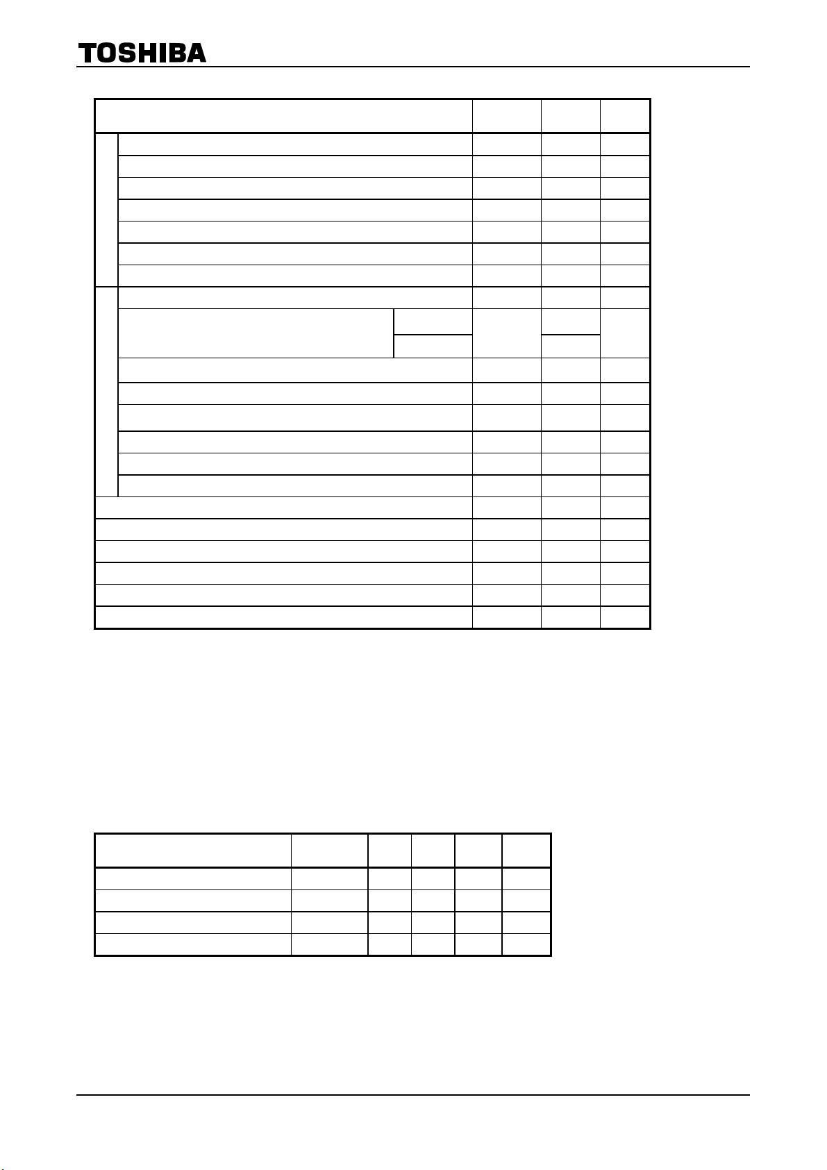
The TOSHIBA TLP3021 (S), TLP3022 (S) and TLP3023 (S) consist of
photo-triac optically coupled to a gallium arsenide infrared emitting diode
in a six lead plastic DIP.
z Peak Off-State Voltage : 400 V (min)
z Trigger LED Current : 15 mA (max) (TLP3021(S))
10 mA (max) (TLP3022(S))
5 mA (max) (TLP3023(S))
z On-State Current : 100 mA (max)
z Isolation Voltage : 5000Vrms(Min)
z UL Recognized : UL1577,File No.E67349
z SEMKO Approved : SS EN60065
SS EN60950, File No.9841105
z BSI Approved : BS EN60065, File No.8385
BS EN60950, File No.8386
z Option (D4) type
VDE approved: DIN EN60747-5-2
Approved No. 40009302
Maximum operating insulation voltage: 890V
Highest permissible over voltage: 8000V
(Note):When a EN60747-5-2 approved type is needed,
please designate the "Option (D4)"
z Construction Mechanical Rating
Creepage Distance
Clearance
Insulation Thickness
7.62 mm pich
Standard Type
7.0 mm (Min)
7.0 mm (Min)
0.5 mm (Min)
PK
10.16 mm pich
TLPxxxxF Type
8.0 mm (Min)
8.0 mm (Min)
0.5 mm (Min)
PK
JEDEC ―
EIAJ ―
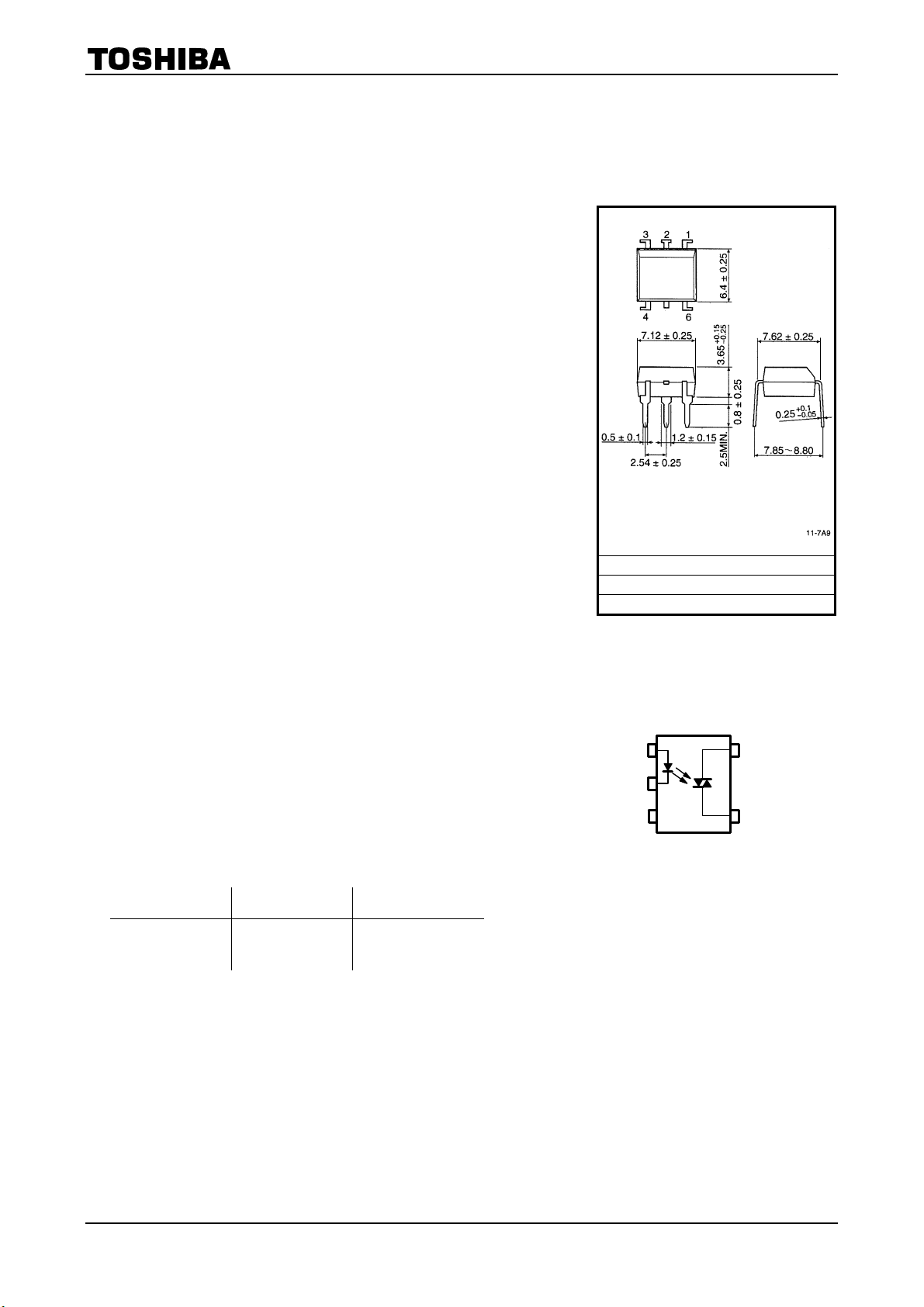
TOSHIBA 11-7A9
Weight : 0.39g
Pin Configuration
(top view)
1
2
3
1: Anode
2: Csthode
3: N.C.
4:Terminal 1
6:Terminal 2
Unit: mm
6
4
1
2007-10-01
Absolute Maximum Ratings (Ta=25°C)
CHARACTERISTIC SYMBOL RATING UNIT
TLP3021(S),TLP3022(S),TLP3023(S)
Forward Current I
Forward Current Derating (Ta≥53°C) ∆IF /°C −0.7 mA /°C
Peak Forward Current (100μs pulse, 100pps) I
LED
Power Dissipation PD 100 mW
Power Dissipation Derating (Ta≥25°C) ∆PD /°C -1.0 mW/°C
Reverse Voltage V
Junction Temperature Tj 125 °C
Off-State Output Terminal Voltage V
On-State RMS Current
On-State Current Derating (Ta≥25°C) ∆IT/°C -1.1 mA /°C
Peak On-State Current (100μs pulse, 120pps) I
Peak Nonrepetitive Surge Current (Pw=10ms,DC=10%) I
DETECTOR
Power Dissipation PD 300
Power Dissipation Derating (Ta≥25°C) ∆PD /°C -4.0
Junction Temperature T
Storage Temperature Range T
Operating Temperature Range T
Lead Soldering Temperature (10s) T
Total Package Power Dissipation PT 330
Total Package Power Dissipation Derating (Ta≥25°C) ∆PT/°C -4.4
Isolation Voltage (AC,1min. , R.H.≤60%) (Note 2) BV
Ta=25°C 100
Ta=70°C
F
FP
R
DRM
I
T(RMS)
TP
1.2 A
TSM
j
stg
opr
sol
S
50 mA
1 A
5 V
400 V
50
2 A
115
−55~150 °C
−40~100 °C
260
5000 Vrms
mA
mW
mW/°C
°C
°C
mW
mW /°C
Note: Using continuously under heavy loads (e.g. the application of high temperature/current/voltage and the
significant change in temperature, etc.) may cause this product to decrease in the reliability significantly even
if the operating conditions (i.e. operating temperature/current/voltage, etc.) are within the absolute maximum
ratings.
Please design the appropriate reliability upon reviewing the Toshiba Semiconductor Reliability Handbook
(“Handling Precautions”/“Derating Concept and Methods”) and individual reliability data (i.e. reliability test
report and estimated failure rate, etc).
(Note 2) Device considered a two terminal device :Pins1,2 and 3 shorted together and pin4 and pin6 shorted
together.
Recommended Operating Conditions
CHARACTERISTIC SYMBOL MIN. TYP. MAX. UNIT
Supply Voltage V
Forward Current I
Peak On-State Current I
Operating Temperature T
AC
F*
TP
opr
Note: Recommended operating conditions are given as a design guideline to obtain expected performance of the
device. Additionally, each item is an independent guideline respectively. In developing designs using this
product, please confirm specified characteristics shown in this document.
*In The case of TLP3022
— —
15 20 25 mA
— —
−25 — 85 °C
120 Vac
1 A
2
2007-10-01
 Loading...