

Page 1

4
查询TLP283供应商
TLP283,TLP283-4
TOSHIBA PHOTOCOUPLER GaAs IRED & PHOTO-TRANSISTOR
TENTATIVE
TLP283,TLP283-4
PROGRAMMABLE CONTROLLERS
AC adapters for PDAs/ on-board power supplies
I/O interface boards
TLP283 and TLP283-4 is a very small and thin coupler,suitable
for surface mount assembly in applications such as on-board power
supplies,programmable controllers.
TLP283 and TLP283-4 consist of photo transistor,optically coupled
to a gallium arsenide infrared emitting diode.
l Collector-Emitter Voltage : 100 V (MIN)
l Current Transfer Ratio : 100% (MIN)@IF=1mA
l 1 Pulse delay time(Note 1)
l Isolation Voltage : 2500 Vrms (MIN)
l UL Recognized : UL1577 , File No. E67349
Note 1 : 1 Pulse delay time = tON+tOFF
: 100us(MAX)@IF=1mA,RL=10kΩ
PIN CONFIGURATION(Top view)
TLP283 TLP283-4
1
4
1
16
TOSHIBA 11-3A1
Weight: 0.05 g
Unit in mm
TLP283
Unit in mm
TLP283-
2
1:ANODE
2:CATHODE
3:EMITTER
4:COLLECTOR
3
2
3
4
5
6
15
14
13
12
11
7 10
8 9
1,3,5,7 :ANODE
2,4,6,8 :CATHODE
9,11,13,15 :EMITTER
10,12,14,16 :COLLECTOR
TOSHIBA 11-10F1
Weight: 0.19 g
1
2002-09-04
Page 2
TLP283,TLP283-4
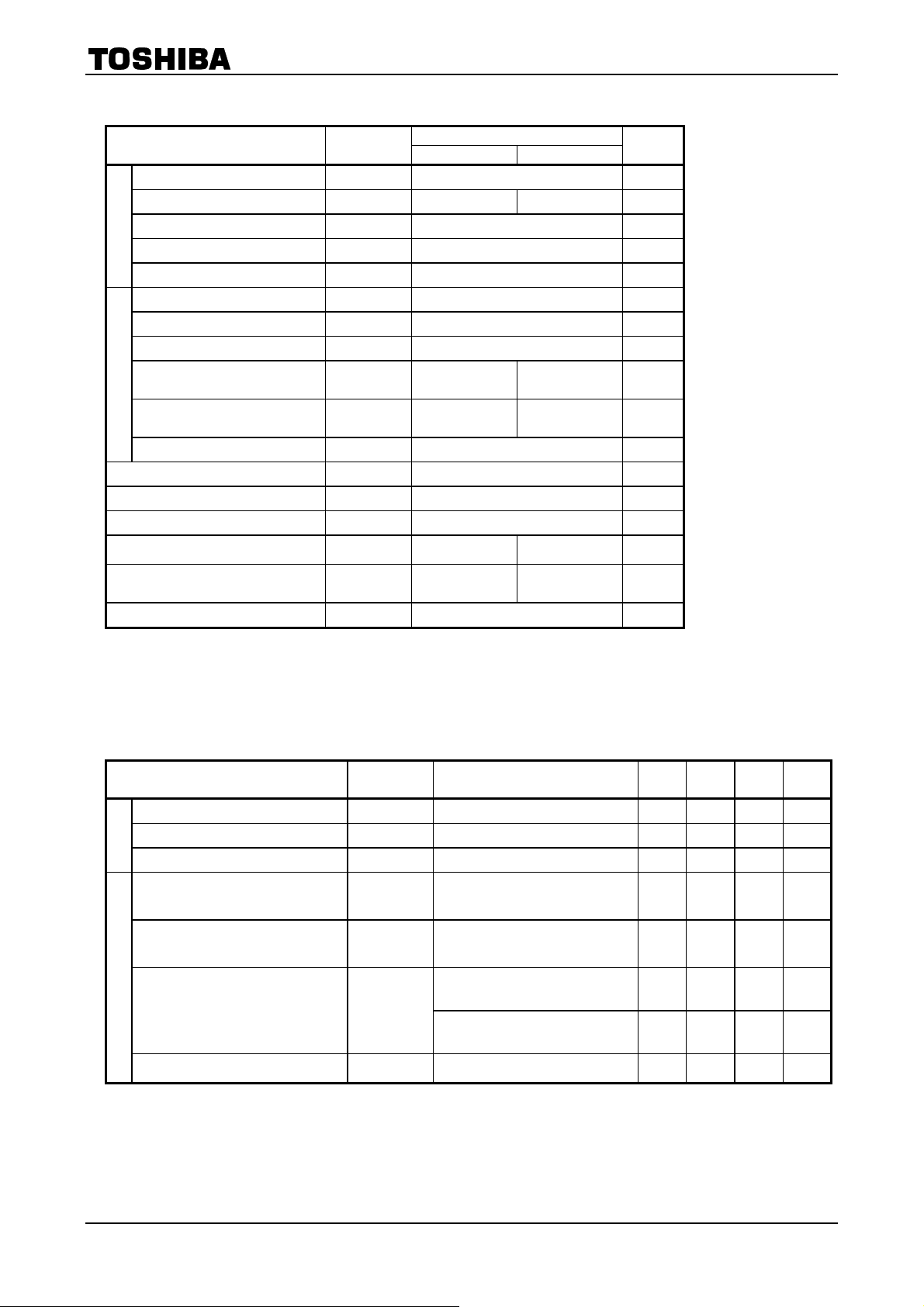
MAXIMUM RATINGS
CHARACTERISTIC SYMBOL
Forward Current IF 50 mA
Forward Current Derating ∆IF /°C −0.7 (Ta≥53°C) −0.5 (Ta≥25°C) mA /°C
Pulse Forward Current IFP 1 A
LED
Reverse Voltage VR 5 V
Junction Temperature Tj 125 °C
Collector-Emitter Voltage V
Emitter-Collector Voltage V
Collector Current IC 50 mA
Collector Power Dissipation
(1 Circuit)
DETECTOR
Collector Power Dissipation
Derating(Ta≥25°C) (1 Circuit)
Junction Temperature Tj 125 °C
Operating Temperature Range T
Storage Temperature Range T
Lead Soldering Temperature T
Total Package Power Dissipation
(1 Circuit)
Total Package Power Dissipation
Derating (Ta≥25°C) (1 Circuit)
Isolation Voltage (Note2) BVS 2500(AC,1min,R.H.≤60%) Vrms
(Ta = 25℃℃℃℃)
∆P
∆P
RATING
TLP283 TLP283−4
100 V
CEO
7 V
ECO
P
150 100 mW
C
/°C −1.5 −1.0 mW /°C
C
−55~100 °C
opr
−55~125 °C
stg
260 (10s) °C
sol
P
200 170 mW
T
/°C −2.0 −1.7 mW /°C
T
UNIT
(Note2)Device considered a two terminal device : LED side pins shorted together and
DETECTOR side pins shorted together.
INDIVIDUAL ELECTRICAL CHARACTERISTICS
(Ta = 25℃℃℃℃)
CHARACTERISTIC SYMBOL TEST CONDITION MIN. TYP. MAX. UNIT
Forward Voltage VF IF = 10 mA 1.0 1.15 1.3 V
Reverse Current IR VR = 5 V
LED
Capacitance CT V = 0, f = 1 MHz
Collector-Emitter
Breakdown Voltage
Emitter-Collector
Breakdown Voltage
Collector Dark Current
DETECTOR
Capacitance
(Collector to Emitter)
(Note3)
V
(BR) CEOIC
V
(BR) ECOIE
I
CEO
C
V = 0, f = 1 MHz
CE
= 0.5 mA 100
= 0.1 mA 7
VCE = 48 V,
Ambient Light Below
(100 ℓx)
V
= 48 V, Ta = 85°C
CE
Ambient Light Below
(100 ℓx)
(Note3) Because of the construction,leak current might be increased by ambient light.
Please use photocoupler with less ambient light.
—
—
—
—
—
— 10 µA
30 — pF
— —
— —
0.01
(2)
(4)
10 — pF
0.1
(10)
2
50
(50)
V
V
µA
µA
2
2002-09-04
Page 3

TLP283,TLP283-4
COUPLED ELECTRICAL CHARACTERISTICS
CHARACTERISTIC SYMBOL TEST CONDITION MIN. TYP. MAX. UNIT
Current Transfer Ratio IC / I
Saturated CTR IC / I
Collector-Emitter
Saturation Voltage
Off-State Collector Current I
V
ISOLATION CHARACTERISTICS
CHARACTERISTIC SYMBOL TEST CONDITION MIN. TYP. MAX. UNIT
Capacitance
(Input to Output)
Isolation Resistance R
Isolation Voltage BV
SWITCHING CHARACTERISTICS
F (sat)
CE (sat) IC
C (off)
(Ta = 25℃℃℃℃)
C
(Ta = 25℃℃℃℃)
IF = 1 mA, VCE = 5 V 100
F
IF = 1 mA, VCE = 0.4 V 50 —
= 0.2 mA, IF = 1 mA
VF = 0.7 V, VCE = 48 V
VS = 0 V, f = 1 MHz — 0.8
S
VS = 500 V, R.H.≤60% 5×10
S
AC , 1 minute 2500 —
AC , 1 second,in OIL
S
DC , 1 minute, in OIL
(Ta = 25℃℃℃℃)
400 %
—
%
pF
Ω
Vrms
Vdc
0.2 0.4 V
—
—
—
10
14
10
5000
—
5000
—
—
10 µA
—
—
—
—
—
CHARACTERISTIC SYMBOL TEST CONDITION MIN. TYP. MAX. UNIT
Turn-On Time t
Turn-Off Time t
1 Pulse delay time t
(Fig.1)SWITCHING TIME TEST CIRCUIT
ON
OFF
ON+ tOFF
VCC = 5 V, IF = 1 mA
R
= 10kΩ
L
—
—
—
7.5
70
80
20
90
100
µs
3
2002-09-04
Page 4

TLP283,TLP283-4
RESTRICTIONS ON PRODUCT USE
· TOSHIBA is continually working to improve the quality and reliability of its products. Nevertheless, semiconductor
devices in general can malfunction or fail due to their inherent electrical sensitivity and vulnerability to physical
stress. It is the responsibility of the buyer, when utilizing TOSHIBA products, to comply with the standards of
safety in making a safe design for the entire system, and to avoid situations in which a malfunction or failure of
such TOSHIBA products could cause loss of human life, bodily injury or damage to property.
In developing your designs, please ensure that TOSHIBA products are used within specified operating ranges as
set forth in the most recent TOSHIBA products specifications. Also, please keep in mind the precautions and
conditions set forth in the “Handling Guide for Semiconductor Devices,” or “TOSHIBA Semiconductor Reliability
Handbook” etc..
· The TOSHIBA products listed in this document are intended for usage in general electronics applications
(computer, personal equipment, office equipment, measuring equipment, industrial robotics, domestic appliances,
etc.). These TOSHIBA products are neither intended nor warranted for usage in equipment that requires
extraordinarily high quality and/or reliability or a malfunction or failure of which may cause loss of human life or
bodily injury (“Unintended Usage”). Unintended Usage include atomic energy control instruments, airplane or
spaceship instruments, transportation instruments, traffic signal instruments, combustion control instruments,
medical instruments, all types of safety devices, etc.. Unintended Usage of TOSHIBA products listed in this
document shall be made at the customer’s own risk.
· Gallium arsenide (GaAs) is a substance used in the products described in this document. GaAs dust and fumes
are toxic. Do not break, cut or pulverize the product, or use chemicals to dissolve them. When disposing of the
products, follow the appropriate regulations. Do not dispose of the products with other industrial waste or with
domestic garbage.
· The products described in this document are subject to the foreign exchange and foreign trade laws.
000707EBC
· The information contained herein is presented only as a guide for the applications of our products. No
responsibility is assumed by TOSHIBA CORPORATION for any infringements of intellectual property or other
rights of the third parties which may result from its use. No license is granted by implication or otherwise under
any intellectual property or other rights of TOSHIBA CORPORATION or others.
· The information contained herein is subject to change without notice.
4
2002-09-04
 Loading...