

现货库存、技术资料、百科信息、热点资讯,精彩尽在鼎好!
TOSHIBA Photocoupler GaAs Ired & Photo−MOS FET / Photo−Transistor
TENTATIVE
TLP270D
TLP270D
Mobile / Note PCs
PDAs
Multimedia TVs
Modems
TLP270D has many multi−functions in DAA circuits for modems,
which is a fully integrated design photocoupler in a 14pin(SOP16).
(1) Photorelay
Dial pulsing switch, hookswitch
· 1 form A
· Peak off−state voltage: 200V (min.)
· Trigger LED current: 3mA (max.)
· On−state current: 150mA (max.)
(2) Photocoupler
Ring detection
· Collector−emitter voltage: 80V (min.)
· Current transfer ratio: 50% (min.)
(3) Darlington transistor
Electronic inductor
· Collector―emitter voltage: 30V (min.)
· Collector current: 150mA (max.)
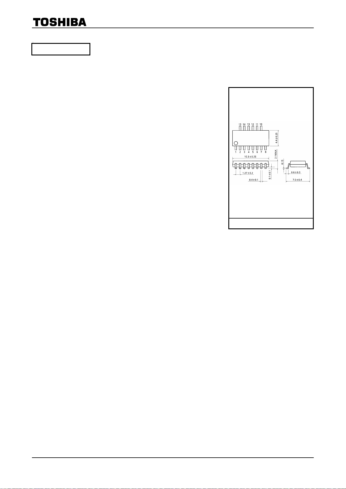
Unit in mm
TOSHIBA
Weight: 0.2g
1
2002-09-25
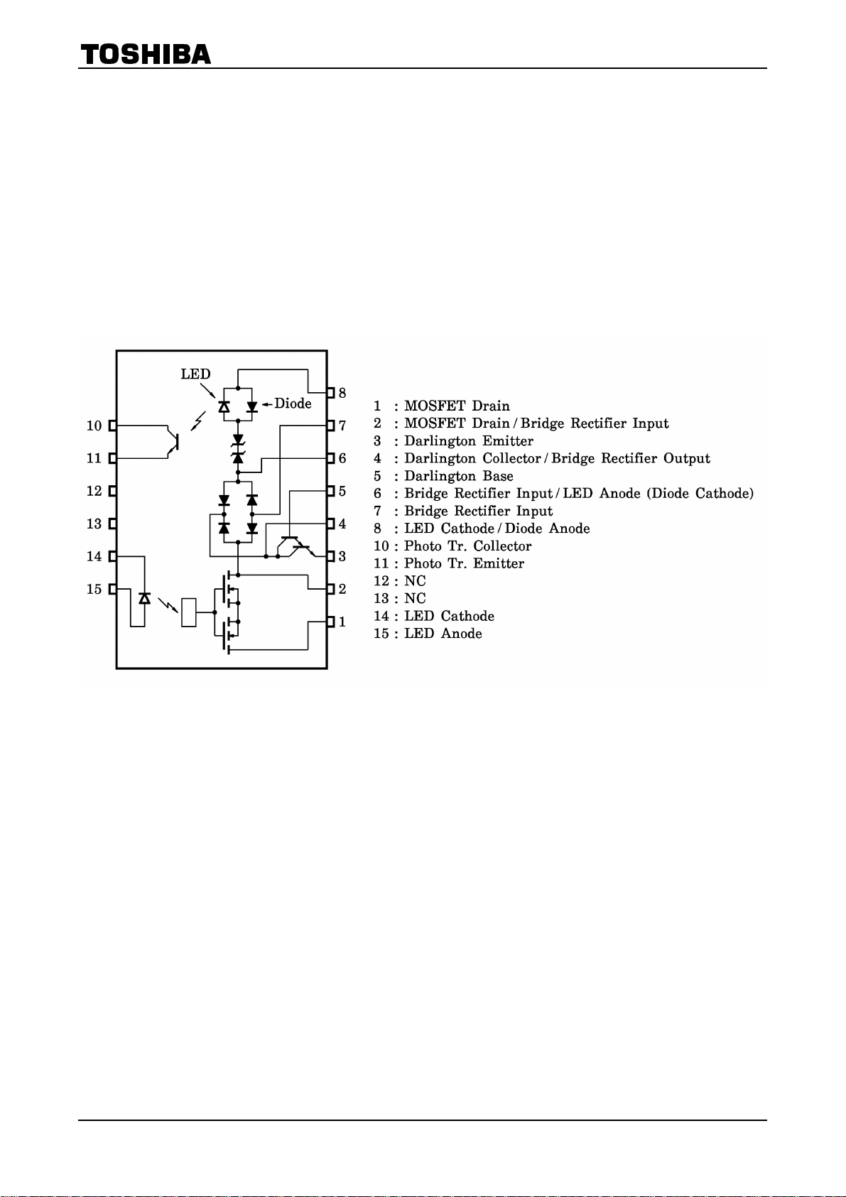
(4) Bridge rectifier
Polarity protection
· Reverse voltage: 30V (min.)
· Forward voltage: 1.7V (max.)
(5) Zener diode
Ring detection protector
· Zener voltage: 22~32V
(Common)
· Isolation voltage: 1500Vrms (min.)
· UL recognized: UL1577, file No. E67349
Pin Configuration
(top view)
TLP270D
2
2002-09-25
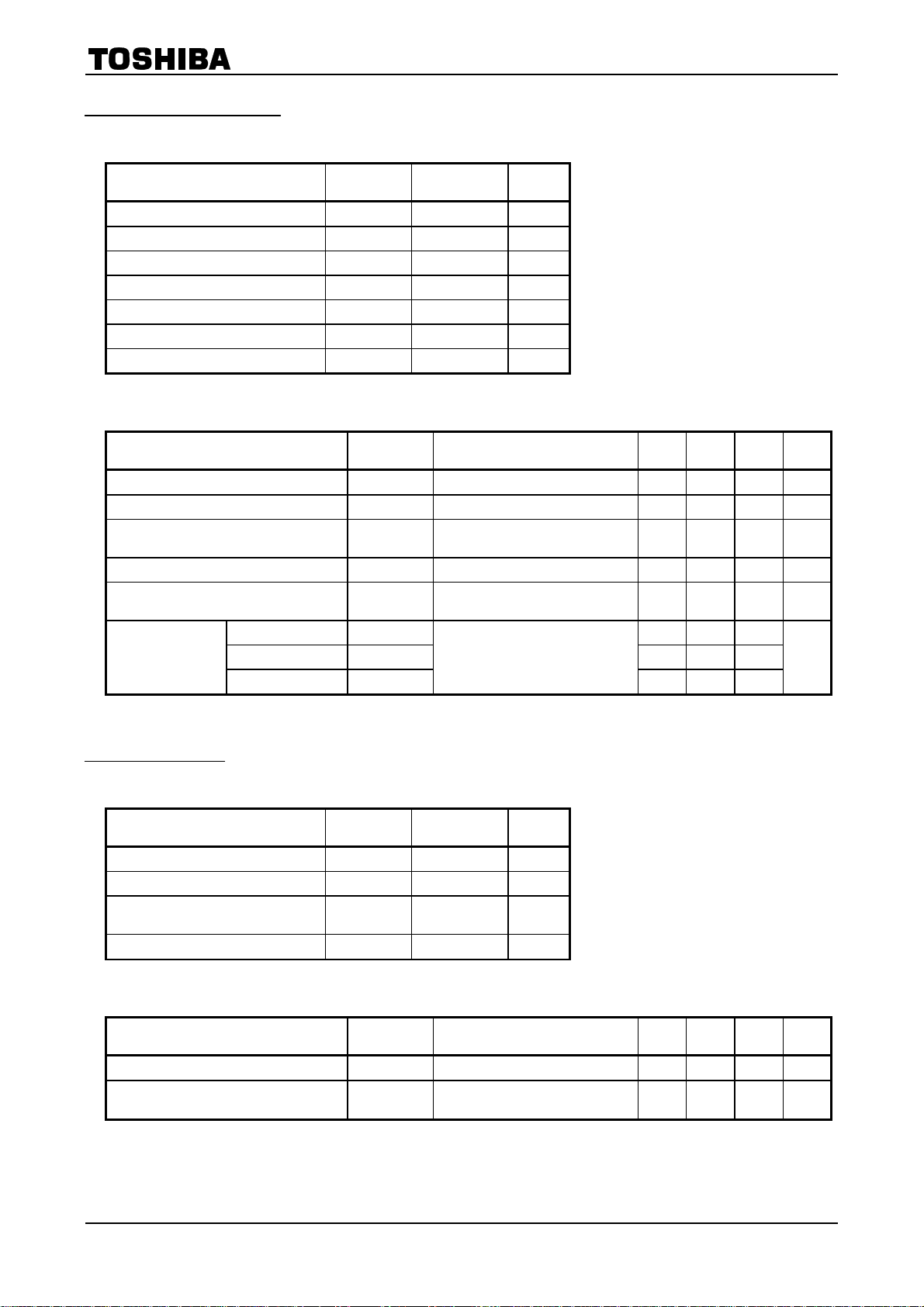
TLP270D
Photorelay
(1----form----A)
Maximum Ratings
Characteristic Symbol Rating Unit
Forward current IF 50 mA
Forward current derating
(Ta ≥ 25°C)
Peak forward current
LED
(100ms pulse, 100pps)
Reverse voltage VR 5 V
Junction temperature Tj 125 °C
Off-state output terminal
voltage
On-state RMS current ION 150 mA
On-state RMS current
Detector
derating(Ta ≥ 25°C)
Junction temperature Tj 125 °C
(Ta = 25°C)
∆I
/ °C -0.5 mA / °C
F
I
1 A
FP
V
200 V
OFF
∆I
/ °C -1.5 mA / °C
ON
Individual Electrical Characteristics
(Ta = 25°C)
Characteristic Symbol Test Condition Min. Typ. Max. Unit
Forward voltage VF IF=10mA 1.0 1.15 1.3 V
Reverse current IR VR=5V ― ― 10 mA
LED
Capacitance CT V=0, f=1MHz ― 30 ― pF
Off-state current I
Detector
Capacitance C
V
OFF
V=0, f=1MHz ― 90 ― pF
OFF
=200V ― ― 1 mA
OFF
Coupled
Trigger LED current IFT ION=150mA ― 1 3 mA
On-state resistance RON ION=150mA, IF=5mA ― 5 8 W
Electrical Characteristics
Characteristic Symbol Test Condition Min. Typ. Max. Unit
(Ta = 25°C)
Switching Characteristics
Characteristic Symbol Test Condition Min. Typ. Max. Unit
Turn-on time tON ― ― 1.5
Turn-off time t
(Ta = 25°C)
OFF
R
=200W, VCC=20V,
L
=5mA
I
F
― ― 1
ms
3
2002-09-25
TLP270D
Photocoupler
Maximum Ratings
Forward current IF ±50 mA
Forward current derating
(Ta ≥ 25°C)
LED
Pulse forward current
(100ms pulse,100pps)
Junction temperature Tj 125 °C
Collector-emitter voltage V
Emitter-collector voltage V
Collector current IC 50 mA
Collector power dissipation
(1 circuit)
Detector
Collector power dissipation
derating(Ta ≥ 25°C) (1 circuit)
Junction temperature Tj 125 °C
(AC----input transistor output)
(Ta = 25°C)
Characteristic Symbol Rating Unit
∆I
/ °C -0.5 mA / °C
F
I
1 A
FP
80 V
CEO
7 V
ECO
P
150 mW
C
∆P
/ °C -1.5 mW / °C
C
Individual Electrical Characteristics
(Ta = 25°C)
Characteristic Symbol Test Condition Min. Typ. Max. Unit
Forward voltage VF IF=±10mA 1.0 1.15 1.3 V
LED
Capacitance CT V=0, f=1MHz ― 60 ― pF
Collector-emitter
breakdown voltage
Emitter-collector
breakdown voltage
Detector
Collector dark current ID
Capacitance CCE V=0, f=1MHz ― 10 ― pF
V
(BR)CEO
V
(BR)ECO
IC=0.5mA 80 ― ― V
IE=0.1mA 7 ― ― V
VCE=48V
(ambient light: 100 lx)
=48V, Ta=85°C
V
CE
(ambient light: 100 lx)
― ― 0.01
(2)
―
―
(4)
0.1
(20)
2
50
(50)
mA
mA
4
2002-09-25

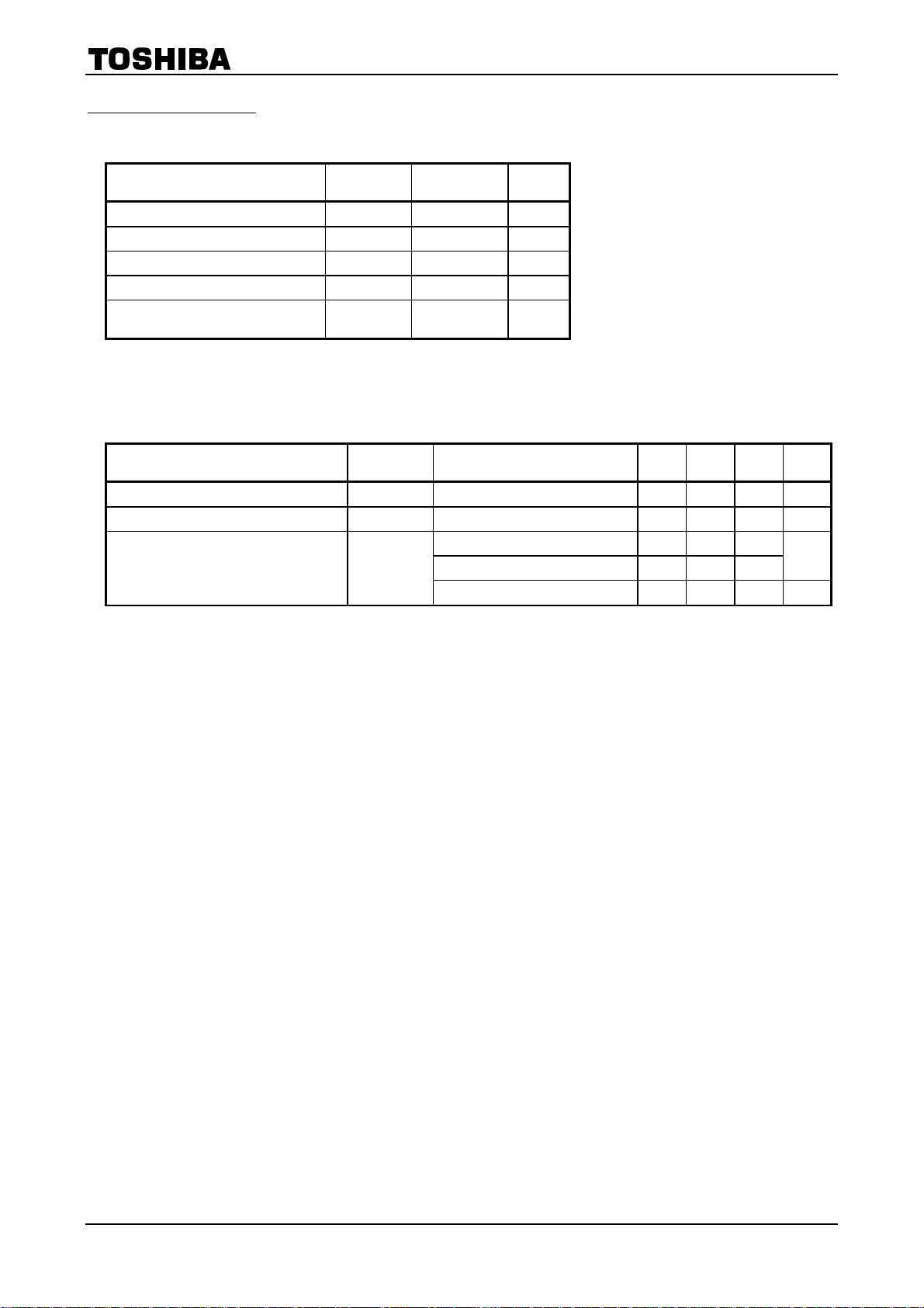
TLP270D
Coupled Electrical Characteristics
Characteristic Symbol Test Condition Min. Typ. Max. Unit
Current transfer ratio
(CTR)
Saturated CTR
Collector-emitter saturation
voltage
Off-state collector current I
I
I
V
CE(sat)
(Ta = 25°C)
C/ IF
C/ IF
(sat)
VF=0.7V, VCE=48V ― ― 10 mA
C(off)
I
=5mA, VCE=5V
F
=1mA, VCE=0.4V
I
F
IC=2.4mA, IF=8mA ― ― 0.4
I
=0.2mA, IF=1mA
C
Rank GB
Rank GB
Rank GB
50 ― ―
100 ― ―
― 60 ―
30 ― ―
― 0.2 ―
― ― 0.4
Switching Characteristics
Characteristic Symbol Test Condition Min. Typ. Max. Unit
Rise time tr ― 2 ―
Fall time tf ― 3 ―
Turn-on time ton ― 3 ―
Turn-off time t
Turn-on time tON ― 2 ―
Storage time ts ― 25 ―
Turn-off time t
(Ta = 25°C)
off
OFF
V
=10V, IC=2mA,
CC
R
=100W
L
=1.9kW, VCC=5V,
R
L
I
=16mA
F
― 3 ―
― 40 ―
Zener Diode
%
%
V
ms
Individual Electrical Characteristics
Characteristic Symbol Test Condition Min. Typ. Max. Unit
Zener voltage VZ ― 22 27 32 V
(Ta = 25°C)
5
2002-09-25
Darlington Transistor
TLP270D
Maximum Ratings
Characteristic Symbol Rating Unit
Collector-base voltage V
Collector-emitter voltage V
Emitter-base voltage V
Collector current IC 0.15 A
Base current IB 20 mA
Collector power dissipation PC 350 mW
Junction temperature Tj 125 °C
(Ta = 25°C)
30 V
CBO
30 V
CEO
10 V
EBO
Individual Electrical Characteristics
Characteristic Symbol Test Condition Min. Typ. Max. Unit
Collector off current I
Emitter off current I
Collector-emitter breakdown
voltage
DC current gain hFE VCE=2V, IC=150mA 4000 ― ―
Collector-emitter saturation
voltage
Turn-on time ton ― 0.20 ―
Switching
time
Storage time t
Fall time t
(Ta = 25°C)
VCB=30V, IE=0 ― ― 10 mA
CBO
VEB=10V, IC=0 ― ― 10 mA
EBO
V
V
IC=10mA, IB=0 30 ― ― V
(BR)CEO
IC=0.15A, IB=1mA ― ― 1.5 V
CE(sat)
I
=1mA, VCC=15V,
B
― 0.6 ―
stg
f
R
L
=15W
― 0.3 ―
Bridge Rectifier
ms
Maximum Ratings
Characteristic Symbol Rating Unit
Repetitive peak reverse voltage V
Average output rectified current IO 0.15 A
Peak one cycle surge forward
current
Junction temperature Tj 125 °C
(Ta = 25°C)
30 V
RRM
I
0.5 A
FSM
Individual Electrical Characteristics
Characteristic Symbol Test Condition Min. Typ. Max. Unit
Forward voltage VFM IFM=0.12A ― ― 1.7 V
Repetitive peak reverse
current
(Ta = 25°C)
I
V
RRM
RRM
=rated ― ― 10 mA
6
2002-09-25
TLP270D
Package
(common)
Maximum Ratings
Characteristic Symbol Rating Unit
Total package power dissipation PT 650 mW
Storage temperature range T
Operating temperature range T
Lead soldering temperature(10s) T
Isolation voltage
(AC, 1min., R.H.≤ 60%) (Note 1)
(Note 1): Device considered a two-terminal device: Pins1, 2, 3, 4, 5, 6, 7 and 8 shorted together and pins 10, 11, 12,
13, 14 and 15 shorted together.
Isolation Characteristics
Characteristic Symbol Test Condition Min. Typ. Max. Unit
Capacitance input to output CS VS=0, f=1MHz ― 0.8 ― pF
Isolation resistance RS VS=500V, R.H.≤ 60% 5 ´ 1010 1014 ― W
Isolation voltage BVS
(Ta = 25°C)
(Ta = 25°C)
-55~100 °C
stg
-20~85 °C
opr
260 °C
sol
BV
1500 Vrms
S
AC, 1 minute 1500 ― ―
AC, 1 second, in oil ― 3000 ―
DC, 1 minute, in oil ― 3000 ― Vdc
Vrms
7
2002-09-25

TLP270D
RESTRICTIONS ON PRODUCT USE
· TOSHIBA is continually working to improve the quality and reliability of its products. Nevertheless, semiconductor
devices in general can malfunction or fail due to their inherent electrical sensitivity and vulnerability to physical
stress. It is the responsibility of the buyer, when utilizing TOSHIBA products, to comply with the standards of
safety in making a safe design for the entire system, and to avoid situations in which a malfunction or failure of
such TOSHIBA products could cause loss of human life, bodily injury or damage to property.
In developing your designs, please ensure that TOSHIBA products are used within specified operating ranges as
set forth in the most recent TOSHIBA products specifications. Also, please keep in mind the precautions and
conditions set forth in the “Handling Guide for Semiconductor Devices,” or “TOSHIBA Semiconductor Reliability
Handbook” etc..
· The TOSHIBA products listed in this document are intended for usage in general electronics applications
(computer, personal equipment, office equipment, measuring equipment, industrial robotics, domestic appliances,
etc.). These TOSHIBA products are neither intended nor warranted for usage in equipment that requires
extraordinarily high quality and/or reliability or a malfunction or failure of which may cause loss of human life or
bodily injury (“Unintended Usage”). Unintended Usage include atomic energy control instruments, airplane or
spaceship instruments, transportation instruments, traffic signal instruments, combustion control instruments,
medical instruments, all types of safety devices, etc.. Unintended Usage of TOSHIBA products listed in this
document shall be made at the customer’s own risk.
· Gallium arsenide (GaAs) is a substance used in the products described in this document. GaAs dust and fumes
are toxic. Do not break, cut or pulverize the product, or use chemicals to dissolve them. When disposing of the
products, follow the appropriate regulations. Do not dispose of the products with other industrial waste or with
domestic garbage.
· The products described in this document are subject to the foreign exchange and foreign trade laws.
000707EBC
· The information contained herein is presented only as a guide for the applications of our products. No
responsibility is assumed by TOSHIBA CORPORATION for any infringements of intellectual property or other
rights of the third parties which may result from its use. No license is granted by implication or otherwise under
any intellectual property or other rights of TOSHIBA CORPORATION or others.
· The information contained herein is subject to change without notice.
8
2002-09-25
 Loading...