

现货库存、技术资料、百科信息、热点资讯,精彩尽在鼎好!
TOSHIBA photocoupler GaAℓAs IRed & Photo IC
TLP2631
Isolated Line Receiver
Simplex / Multiplex Data Transmission
Computer-Peripheral Interface
Microprocessor System Iinterface
Digital Isolation For A / D, D / A Conversion
The TOSHIBA TLP2631 dual photocoupler consists of a pair of GaAℓAs
light emitting diode and integrated high gain, high speed photodetector.
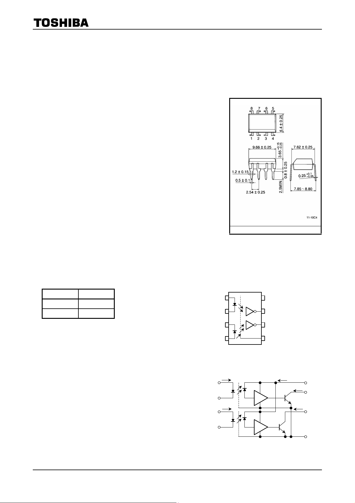
This unit is 8-lead DIP.
The output of the detector circuit is an open collector, Schottky clamped
transistor.
A Faraday shield integrated on the photodetector chip reduces the effects
of capacitive coupling between the input LED emitter and the high gain
stages of the detector. This provides an effective common mode transient
immunity of 1000V / μs.
• Input current
• Switching speed: 10MBd(typ.)
• Common mode transient immunity: ±1000V / μs(min.)
• Guaranteed performance over temperature: 0~70°C
• Isolation voltage: 2500V
• UL recognized: UL1577, file no. E67349
Truth Table
threshold: I
= 5mA(max.)
F
(min.)
rms
(positive logic)
Pin Configuration (top view)
TLP2631
Unit in mm
TOSHIBA 11−10C4
Weight: 0.54g
Input Output
H L
L H
A 0.01 to 0.1μF bypass capacitor must
connected between pins 8 and 5(see Note 1).
1
2
3
4
Schematic
I
F1
1
+
V
F1
2
−
I
F2
4
+
V
F2
3
−
Shield
Shield
VCC
GND
1 : Anode 1
8
2 : Cathode 1
3 : Cathode 2
7
4 : Anode 2
5 : GND
6
6 : V
O2
7 : V
5
O1
8 : V
CC
ICC
(Output 2)
(Output 1)
8
V
I
O1
7
V
I
O2
6
V
5
GND
CC
O1
O2
1
2007-10-01
TLP2631
Absolute Maximum Ratings
Characteristic Symbol Rating Unit
Forward current (each channel) I
Pulse forward current
LED
(each channel)*
Reverse voltage (each channel) VR 5 V
Output current (each channel) I
Output voltage (each channel) VO −0.5~7 V
Supply voltage
(1 minute maximum)
Detector
Output collector power
dissipation (each channel)
Operating temperature range T
Storage temperature range T
Lead soldering temperature
(10s)**
Isolation voltage
(AC, 1 min., R.H.≤ 60%, Note 3)
(no derating required up to 70°C)
F
I
30 mA
FP
O
V
7 V
CC
P
40 mW
O
−55~125 °C
stg
−40~85 °C
opr
T
260 °C
sol
BV
2500 Vrms
S
20 mA
16 mA
Note: Using continuously under heavy loads (e.g. the application of high temperature/current/voltage and the
significant change in temperature, etc.) may cause this product to decrease in the reliability significantly even
if the operating conditions (i.e. operating temperature/current/voltage, etc.) are within the absolute maximum
ratings and the operating ranges.
Please design the appropriate reliability upon reviewing the Toshiba Semiconductor Reliability Handbook
(“Handling Precautions”/“Derating Concept and Methods”) and individual reliability data (i.e. reliability test
report and estimated failure rate, etc).
* t ≤ 1 msec duration.
** 2mm below seating plane.
Recommended Operating Conditions
Characteristic Symbol Min. Typ. Max. Unit
Input current, low level, each channel IFL 0 ― 250 μA
Input current, high level, each channel IFH 6.3* ― 20 mA
Supply voltage**, output VCC 4.5 5 5.5 V
Fan out (TTL load, each channel) N ― ― 8
Operating temperature T
Note: Recommended operating conditions are given as a design guideline to obtain expected performance of the
device. Additionally, each item is an independent guideline respectively. In developing designs using this
product, please confirm specified characteristics shown in this document.
0 ― 70 °C
opr
*6.3mA is a guard banded value which allows for at least 20% CTR degradation.
Initial input current threshold value is 5.0mA or less.
**This item denotes operating ranges, not meaning of recommended operating conditions.
2
2007-10-01
Electrical Characteristics
Characteristic Symbol Test Condition Min. Typ. * Max. Unit
Input forward voltage
(each channel)
(Ta = 0~70°C unless otherwise noted)
IF = 10mA, Ta = 25°C ― 1.65 1.75 V
V
F
TLP2631
Input diode temperature
coefficient (each channel)
Input reverse breakdown
voltage (each channel)
Input capacitance
(each channel)
High level output current
(each channel)
Low level output voltage
(each channel)
High level supply current
(both channels)
Low level supply current
(both channels)
Isolation voltage RS VS = 500V, R.H. ≤ 60% (Note 3) 5×10¹⁰ 1014 ― Ω
Capacitance (input−output) CS f = 1MHz (Note 3) ― 0.6 ― pF
Input−input leakage
current
Resistance (input−input) R
Capacitance (input−input) C
* All typical values are at V
= 5V, Ta = 25°C.
CC
/ ΔTa IF = 10mA ― −2.0 ― mV / °C
ΔV
F
IR = 10μA, Ta = 25°C 5 ― ― V
BV
R
VF = 0, f = 1MHz ― 45 ― pF
C
T
= 5.5V, VO = 5.5V
V
CC
I
OH
V
OL
V
I
CCH
V
I
CCL
I
I−I
V
I−I
f = 1MHZ (Note 6) ― 0.25 ― pF
I−I
= 250μA
I
F
= 5.5V, IF = 5mA
V
CC
(sinking) = 13mA
I
OL
= 5.5V, IF = 0 ― 14 30 mA
CC
= 5.5V, IF = 10mA ― 24 38 mA
CC
R.H. ≤ 60%, t = 5s
= 500V (Note 6)
V
I−I
= 500V (Note 6) ― 1011 ― Ω
I−I
― 1 250 μA
― 0.4 0.6 V
― 0.005 ― μA
3
2007-10-01

TLP2631
Switching Characteristics
Characteristic Symbol
Propagation delay time to
low output level
Propagation delay time to
high output level
Output rise time, output
fall time (10~90%)
Common mode transient
immunity at high output
level
Common mode transient
immunity at low output
level
(Ta = 25°C, V
Test
Circuit
HL 1
t
p
LH 1
t
p
, tf 1
t
r
2
CM
H
2
CM
L
CC
= 5V)
Test Condition Min. Typ. Max. Unit
= 0→7.5mA, RL = 350Ω
I
F
= 15pF (each channel)
C
L
= 7.5mA→0, RL = 350Ω
I
F
= 15pF (each channel)
C
L
= 0 7.5mA, RL = 350Ω
I
F
= 15pF (each channel)
C
L
I
= 0, RL = 350Ω
F
= 400V,
V
CM
(min.) = 2V
V
O
(each channel, Note 4)
I
= 7.5mA, RL = 350Ω
F
= 400V
V
CM
(max.) = 0.8V
V
O
(each channel, Note 5)
― 60 75 ns
― 60 75 ns
― 30 ― ns
1000 10000 ― V / μs
−1000 −10000 ― V / μs
(Note 1) 2mm below seating plane
(Note 2) The VCC supply voltage to each TLP2631 isolator must be bypassed by a 0.01μF capacitor or larger. This
can be either a ceramic or solid tantalum capacitor with good high frequency characteristic and should
be connected as close as possible to the package V
and GND pins each device.
CC
(Note 3) Device considered a two−terminal device: Pins 1, 2, 3 and 4 shorted together, and pins 5, 6, 7 and 8
shorted together.
(Note 4) CM
・the maximum tolerable rate of rise of the common mode voltage to ensure the output will remain in
H
the high state (i.e., V
OUT
> 2.0V).
Measured in volts per microsecond (V / μs).
Volts/ microsecond can be translated to sinusoidial voltages:
μsV / ==
(dVCM)
dt
fMax.
(p.p.)
V
CM
CM
Example:
V
= 319Vpp when f
CM
= 1MHz using CML and CMH = 1000V / μs data sheet specified minimum.
CM
(Note 5) CML・the maximum tolerable rate of fall of the common mode voltage to ensure the output will remain in
the low output state (i.e., V
OUT
> 0.8V).
Measured in volts per microsecond (V / μs).
(Note 6) Measured between pins 1 and 2 shorted together, and pins 3 and 4 shorted together.
4
2007-10-01

Test Circuit 1. tpHL and tpLH
TLP2631
Pulse input
PW = 10μs
Duty cycle = 1/10
Monitor
I
F
* C
is approximately 15pF which includes probe and stray
L
wiring capacitance.
1
2
3
100Ω
4
VCC
GND
8
7
6
5
5V
I
F
R
L
350Ω
0.1μF
C
L
Monitor
V
O
V
O
Test Circuit 2. Transient Immunity And Typical Waveforms.
IF
1
2
B
A
V
FF
3
4
Pulse generator
Z
50Ω
O =
VCC
8
7
6
5
GND
V
CM
+
−
0.1μF
C
L
V
R
350Ω
O
5V
L
Monitor
V
CM
V
O
(IF = 0mA)
V
O
= 7.5mA)
(I
F
7.5mA
3.75mA
0mA
t
r
t
pHL
t
r
90%
10%
tf
5V
4.5V
1.5V
0.5V
t
pLH
tf
V
OL
400V
0V
5V
2V
0.8V
V
OL
CM
* C
CM
L
320(V)
=,
)(
μsrt
320(V)
=
H
)(
μsrt
is approximately 15pF which includes probe and stray
L
wiring capacitance.
5
2007-10-01

TLP2631
(mA)
F
Forward current I
100
10
0.1
Ta = 25 °C
1
I
– VF
F
Forward voltage temperature
−2.6
−2.4
−2.2
/ ΔTa (mV / °C)
−2.0
F
−1.8
−1.6
coefficient ΔV
ΔV
/ ΔTa – IF
F
0.01
1.0
1.2
1.4 1.6
1.8
2.0
Forward voltage VF (V)
– IF
V
8
6
(V)
O
4
2
RL = 350Ω
1kΩ
4kΩ
O
VCC = 5 V
Ta = 25 °C
Output voltage V
0
0
2
1
34
6
5
Forward current IF (mA)
−1.4
0.1
0.3
1
3
10
30
50
Forward current IF (mA)
– Ta
I
100
50
(μA)
30
OH
10
5
3
OH
IF = 250 μA
VCC = 5.5 V
VO = 5.5 V
High level output current I
1
10
0
20
30 40
50
60
70
Ambient temperature Ta (°C)
20
V
OL
– Ta
40
IF = 5 mA
VCC = 5.5 V
VE = 2 V
IOL=16mA
12.8mA
9.6mA
6.4mA
60
80
– IF
V
Ta = 70°C
0°C
2
O
VCC = 5 V
34
RL = 350Ω
RL = 4kΩ
5
0.5
(V)
OL
0.4
0.3
Low level output voltage V
0.2
0
6
Ambient temperature Ta (°C)
10
8
(V)
6
O
4
Output voltage V
2
0
0
1
Forward current IF (mA)
6
2007-10-01

t
120
100
(ns)
pLH
t
pHL,
t
80
60
40
pHL, tpLH
Propagation delay time
20
0
5 19
9
7
Forward current IF (mA)
320
VCC = 5 V
IF = 7.5 mA
300
280
(ns)
f
t
r,
80
60
40
Rise, fall time t
20
0
10 20 30
0
– IF
Ta = 25 °C
VCC = 5 V
tf
tf
tf
tr
RL = 4kΩ
1kΩ
350Ω
350Ω
RL = 4kΩ
60
t
pLH
t
pLH
t
pHL
11 13 15 17
– Ta
t
r, tf
40 50
1kΩ
4kΩ
1kΩ
350Ω
350Ω
1kΩ
4kΩ
70
120
100
(ns)
pLH
t
pHL,
t
Propagation delay time
80
60
40
20
0
0
Ambient temperature Ta (°C)
t
pHL, tpLH
10 20 30
– Ta
t
pLH
t
pLH
t
pHL
40 50
Ambient temperature Ta (°C)
RL = 4kΩ
VCC = 5 V
IF = 7.5 mA
TLP2631
350kΩ
1kΩ
350Ω
1kΩ
4kΩ
70
60
7
2007-10-01

TLP2631
RESTRICTIONS ON PRODUCT USE
• The information contained herein is subject to change without notice.
• TOSHIBA is continually working to improve the quality and reliability of its products. Nevertheless, semiconductor
devices in general can malfunction or fail due to their inherent electrical sensitivity and vulnerability to physical
stress. It is the responsibility of the buyer, when utilizing TOSHIBA products, to comply with the standards of
safety in making a safe design for the entire system, and to avoid situations in which a malfunction or failure of
such TOSHIBA products could cause loss of human life, bodily injury or damage to property.
In developing your designs, please ensure that TOSHIBA products are used within specified operating ranges as
set forth in the most recent TOSHIBA products specifications. Also, please keep in mind the precautions and
conditions set forth in the “Handling Guide for Semiconductor Devices,” or “TOSHIBA Semiconductor Reliability
Handbook” etc.
• The TOSHIBA products listed in this document are intended for usage in general electronics applications
(computer, personal equipment, office equipment, measuring equipment, industrial robotics, domestic appliances,
etc.).These TOSHIBA products are neither intended nor warranted for usage in equipment that requires
extraordinarily high quality and/or reliability or a malfunction or failure of which may cause loss of human life or
bodily injury (“Unintended Usage”). Unintended Usage include atomic energy control instruments, airplane or
spaceship instruments, transportation instruments, traffic signal instruments, combustion control instruments,
medical instruments, all types of safety devices, etc.. Unintended Usage of TOSHIBA products listed in his
document shall be made at the customer’s own risk.
• The products described in this document shall not be used or embedded to any downstream products of which
manufacture, use and/or sale are prohibited under any applicable laws and regulations.
• The information contained herein is presented only as a guide for the applications of our products. No
responsibility is assumed by TOSHIBA for any infringements of patents or other rights of the third parties which
may result from its use. No license is granted by implication or otherwise under any patents or other rights of
TOSHIBA or the third parties.
20070701-EN
• GaAs(Gallium Arsenide) is used in this product. The dust or vapor is harmful to the human body. Do not break,
cut, crush or dissolve chemically.
• Please contact your sales representative for product-by-product details in this document regarding RoHS
compatibility. Please use these products in this document in compliance with all applicable laws and regulations
that regulate the inclusion or use of controlled substances. Toshiba assumes no liability for damage or losses
occurring as a result of noncompliance with applicable laws and regulations.
8
2007-10-01
 Loading...