

TOSHIBA TLP2105 Technical data
现货库存、技术资料、百科信息、热点资讯,精彩尽在鼎好!
A
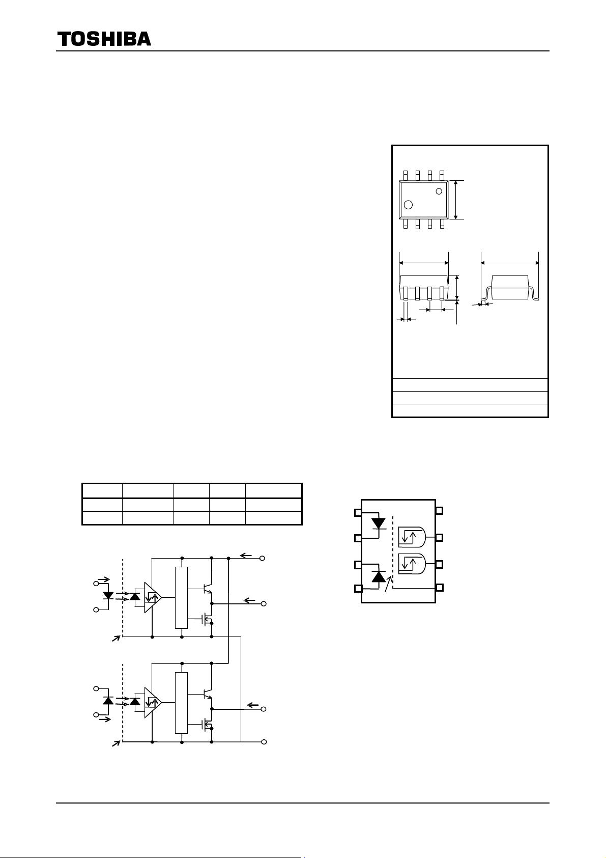
TOSHIBA PHOTOCOUPLER GaAℓAs Ired & PHOTO-IC
TLP2105
Isolated Bus Drivers
TLP2105
Unit: mm
High Speed Line Receivers
Microprocessor System Interfaces
The Toshiba TLP2105 consists of GaAℓAs light emitting diodes and
integrated high gain, high-speed photodetectors.
The TLP2105 is housed in the 8-pin SO package.
The photodetector has totem-pole output stage that can source and sink
current.
The photodetector has an internal Faraday shield that provides a
guaranteed common-mode transient immunity of ±10 kV/μs.
The TLP2105 provides noninverting logic output. An inverting logic
version, the TLP2108, is also available.
z Buffer logic output (totem-pole output)
z Guaranteed performance over -40 to 100°C
z Power supply voltage: 4.5 to 20 V
z Input threshold current: I
z Switching time (t
pLH
/ t
z Common mode transient immunity: ±10 kV/μs
z Isolation voltage: 2500 Vrms
Truth Table
Input LED1(2) Tr1(3) Tr2(4) Output 1(2)
H
L
ON ON OFF
OFF OFF ON
Schematic
I
F1
1
+
VF1
2 -
LED1
=1.6 mA(max)
FLH
): 250 ns (max)
pHL
Tr1
Tr2
I
CC
I
O1
H
1
L
8
V
CC
7
V
O1
2
3
4
8 6 5
7
3.95 ± 0.25
3 4
2
1
5.1 ± 0.2
0.38
2.5 ± 0.2
1.27 ± 0.15
0.1 ± 0.1
6.0 ± 0.2
0.305 min
JEDEC ―
JEITA ―
TOSHIBA 11−5K1
Weight: 0.21 g (typ.)
Pin Configuration (Top View)
SHIELD
V
CC
GND
1: ANODE 1
8
2: CATHODE 1
3: CATHODE 2
7
4: ANODE 2
5: GND
6
6: VO2(Output 2)
7: VO1(Output 1)
5
8: VCC
11- 5K1
SHIELD
LED2
Tr3
Tr4
I
O2
6
V
O2
5
GND
1
2008-11-26
3
-
VF 2
4 +
I
F2
SHIELD
bypass capacitor of 0.1μF must be
connected between pins 8 and 5.
TLP2105
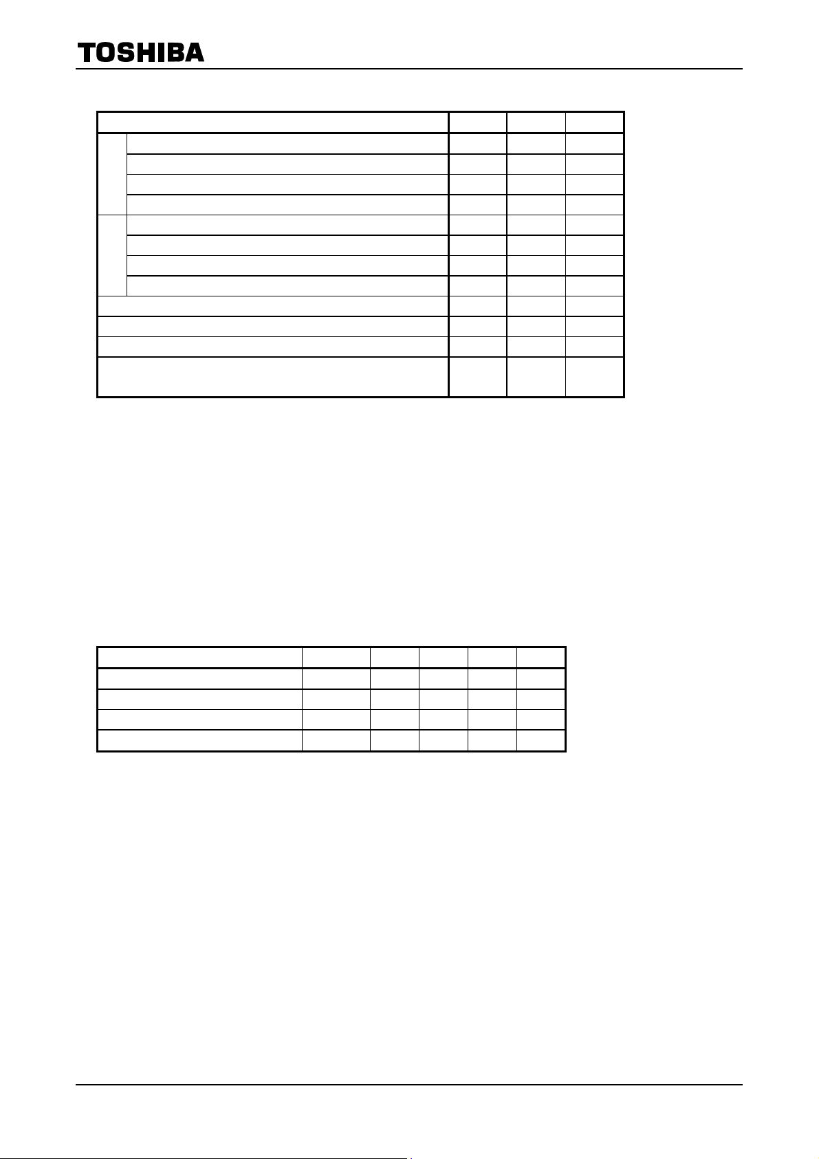
Absolute Maximum Ratings (Ta=25°C)
CHARACTERISTIC SYMBOL RATING UNIT
Forward Current (Note 1) IF 20 mA
Forward current derating (Ta≥75°C) ΔIF/ΔTa -0.48 mA/°C
LED
Peak Transient Forward Current (Note 1,2) I
Reverse Voltage (Note 1) VR 5 V
Output Current 1 (Ta ≤ 25℃) (Note 1) IO1 25/-15 mA
Output Current 2 (Ta = 100℃) (Note 1) IO2 5/-5 mA
Output Voltage (Note 1) VO -0.5 to 20 V
DETECTOR
Supply Voltage VCC -0.5 to 20 V
Operating Temperature Range T
Storage Temperature Range T
Lead Soldering Temperature (10 s) T
Isolation Voltage
(AC,1 min, R.H.
≤ 60%,Ta=25°C) (Note 3)
Note: Using continuously under heavy loads (e.g. the application of high temperature/current/voltage and the
significant change in temperature, etc.) may cause this product to decrease in the reliability significantly even
if the operating conditions (i.e. operating temperature/current/voltage, etc.) are within the absolute maximum
ratings.
Please design the appropriate reliability upon reviewing the Toshiba Semiconductor Reliability Handbook
(“Handling Precautions”/“Derating Concept and Methods”) and individual reliability data (i.e. reliability test
report and estimated failure rate, etc).
Note 1: Each Channel.
Note 2: Pulse width ≤ 1μs, 300 pps.
Note 3: This device is regarded as a two terminal device: pins 1, 2, 3 and 4 are shorted together,
as are pins 5, 6, 7 and 8.
1 A
FPT
-40 to 100 °C
opr
-55 to 125 °C
stg
260 °C
sol
BVs 2500 V
rms
Recommended Operating Conditions
CHARACTERISTIC SYMBOL MIN TYP. MAX UNIT
Input Current , ON I
Input Voltage , OFF V
Supply Voltage* VCC 4.5 ― 20 V
Operating Temperature
2 ― 10 mA
F(ON)
F(OFF)
T
opr
0 ― 0.8 V
-40 ― 100 °C
* This item denotes operating range, not meaning of recommended operating conditions.
Note: Recommended operating conditions are given as a design guideline to obtain expected performance of the
device. Additionally, each item is an independent guideline respectively. In developing designs using this
product, please confirm specified characteristics shown in this document.
2
2008-11-26
Electrical Characteristics
(Unless otherwise specified, Ta=-40 to 100°C, VCC=4.5 to 20 V)
TLP2105
CHARACTERISTIC SYMBOL
Input Forward Voltage VF ― IF=10 mA , Ta=25°C 1.3 1.65 1.75 V
Temperature Coefficient
of Forward Voltage
Input Reverse Current IR ― VR=5 V, Ta=25°C ― ― 10 μ A
Input Capacitance CT ― V=0 , f=1 MHz, Ta=25°C ― 45 ― pF
Logic Low Output Voltage VOL 1 IOL=3.5 mA, VF=0.8 V ― 0.2 0.6 V
Logic High Output Voltage VOH 2
Logic Low Supply Current I
Logic High Supply Current I
Logic Low Short Circuit
Output Current (Note 4)
Logic High Short Circuit
Output Current (Note 4)
Input Current Logic High
Output
Input Voltage Logic Low
Output
Input Current Hysteresis I
*All typical values are at Ta=25°C, V
ΔVF/ΔTa
CCL
CCH
I
OSL
I
OSH
I
FLH
V
FHL
HYS
CC
TEST
CIRCUIT
― I
3 VF=0 V
4 IF1=IF2=5 mA
5 VF=0 V
6
― VCC=5 V ― 0.05 ― mA
― I
― I
=5 V unless otherwise specified
TEST CONDITION MIN TYP. MAX UNIT
=10 mA ― -2.0 ― mV/°C
F
IOH=-2.6 mA,
IF=5 mA
IF=5 mA
=GND
V
O
=-2.6 mA, VO>2.4 V ― 0.4 1.6 mA
O
=3.5 mA, VO<0.6 V 0.8 ― ― V
O
VCC=4.5 V
VCC=20 V 17.4 18.1
VCC=20 V ― ― 6.0
VCC=5.5 V
VCC=20 V ― ― 6.0
VCC=5.5 V
VCC=VO=5.5 V 15
VCC=VO=20 V 20
VCC=5.5 V -5
VCC=20 V -10
2.7 4.0
―
―
― ― 6.0
― ― 6.0
80
90
-15
-20
―
―
―
―
V
mA
mA
mA
mA
Note 4: Duration of output short circuit time should not exceed 10 ms.
Isolation Characteristics
(Ta = 25℃)
CHARACTERISTIC SYMBOL TEST CONDITION MIN TYP. MAX UNIT
Capacitance input to output CS VS = 0, f = 1 MHz (Note 3) ― 0.8 ― pF
12
Isolation resistance R
Isolation voltage BV
S
(Note 3)
AC,1 minute 2500 ― ―
AC,1 second, in oil ― 5000 ―
S
DC,1 minute, in oil ― 5000 ― V
R.H. ≤ 60%, VS = 500 V
1×10
3
14
10
― Ω
V
2008-11-26
rms
dc

TLP2105
A
A
A
A
Switching Characteristics
(Unless otherwise specified, Ta=-40 to 100℃、VCC=4.5 to 20 V)(Each Channel)
|
I
CCL
-
TEST
CIRCUIT
7,8
I
O
V
O
TEST CONDITION MIN TYP. MAX UNIT
IF=0→3 mA
IF=3→0 mA
―
=0→3 mA , VCC=5 V ― 30 75 ns
F
IF=3→0 mA , VCC=5 V ― 30 75 ns
VCM=1000 V
VCC=20 V, Ta=25°C
9
VCM=1000 V
VCC=20 V, Ta=25°C
, IF=5 mA,
p-p
, IF=0 mA,
p-p
IF
1
2
V
V
CC
OL
V
3
4
1
I
F1
2
I
IF
3
F2
1
V
CC
2
V
CC
3
4
30 150 250 ns
30 150 250 ns
― ― 220 ns
-10000
10000
― ― V/μs
― ― V/μs
8
VCC
7
6
0.1 μF
5
GND
SHIELD
Test Circuit
CCH
VCC
8
I
CCH
7
0.1 μF
6
5 4
GND
SHIELD
Test Circuit
OSH
8
VCC
7
I
OSH
0.1 μF
SHIELD
GND
6
5
IO
V
O
V
V
CC
V
O
CHARACTERISTIC SYMBOL
Propagation Delay Time
to Logic High output
Propagation Delay Time
to Logic Low output
Switching Time Dispersion
between ON and OFF
Rise Time (10 – 90 %) tr I
Fall Time (90 – 10 %) tf
Common Mode transient
Immunity at High Level Output
Common Mode transient
Immunity at Low Level Output
t
pLH
t
pHL
|t
pHL
t
pLH
CMH
CML
*All typical values are at Ta=25°C
Note 5: A ceramic capacitor (0.1 μA) should be connected from pin 8 to pin 5 to stabilize the operation of the high gain
linear amplifier. Failure to provide the bypassing may impair the switching property. The total lead length between
capacitor and coupler should not exceed 1 cm.
TEST CIRCUIT 1: VOL Test Circuit TEST CIRCUIT 2: VOH Test Circuit
VF
TEST CIRCUIT 3: I
TEST CIRCUIT 5: I
1
V
2
CC
3
4
SHIELD
CCL
1
2
5
GND
Test Circuit TEST CIRCUIT 4: I
8
V
CC
7
3 6
4
SHIELD
OSL
5
GND
Test Circuit TEST CIRCUIT 6: I
1
V
CC
2
3
4
GND
SHIELD
8
7
6
8
7
6
5
0.1 μF
0.1 μF
I
OSL
0.1 μF
V
CC
V
CC
4
2008-11-26
 Loading...