

TOSHIBA TLP191B Technical data
现货库存、技术资料、百科信息、热点资讯,精彩尽在鼎好!
TOSHIBA Photocoupler GaAℓAs Ired & Photo-Diode Array
TLP191B
TLP191B
Telecommunication
Programmable Controllers
Mos Gate Driver
MOS FET Gate Driver
The TOSHIBA mini flat coupler TLP191B is a small outline coupler,
suitable for surface mount assembly.
The TLP191B consists of a GaAℓAs light emitting diode, optically
coupled to a series connected photo diode array with shunt resistor
which is suitable for MOS FET gate drive.
• Open voltage: 7.0V(min.)
• Short current: 24.0 μA (min.)
• Isolation voltage: 2500 Vrms (min.)
• UL recognized: UL1577,file no.E67349
Absolute Maximum Ratings (Ta = 25°C)
Characteristic Symbol Rating Unit
Forward current IF 50 mA
Forward current
derating (Ta ≥ 25°C)
LED
Detector
Storage temperature range T
Operating temperature range T
Lead soldering temperature (10s) T
Isolation voltage
(AC, 1 min., R.H. ≤ 60%) (Note)
Pulse forward current
(100μs pulse, 100 pps)
Reverse voltage VR 3 V
Junction temperature T
Forward current IFD 50 μA
Reverse voltage VRD 10 V
Junction temperature T
/ °C −0.5 mA / °C
ΔI
F
1 A
I
FP
125 °C
j
125 °C
j
−55~125 °C
stg
−40~80 °C
opr
260 °C
sol
2500 Vrms
BV
S
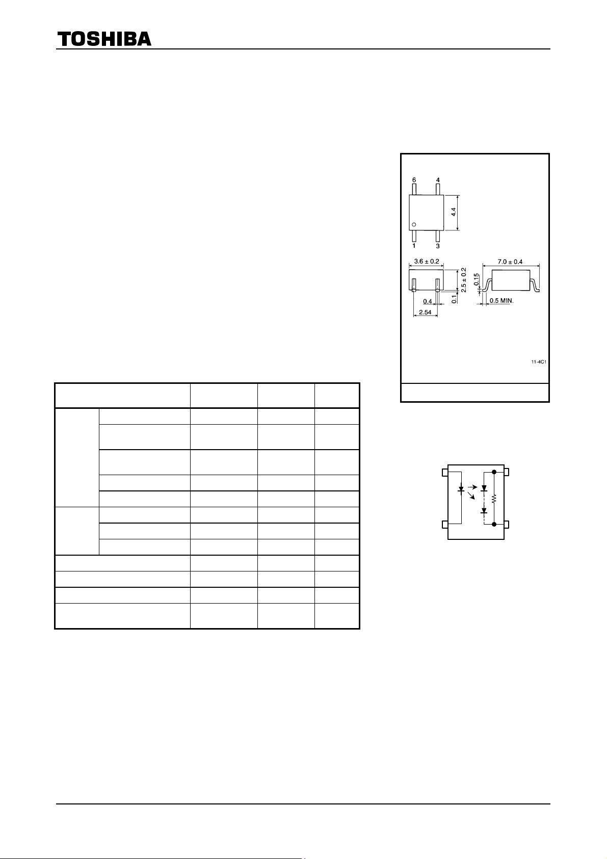
Unit in mm
TOSHIBA 11−4C1
Weight: 0.09 g
Pin Configuration(top view)
1
3
1 . Anode
3 . Cathode
4 . Cathode
6 . Anode
6
4
Note: Using continuously under heavy loads (e.g. the application of high temperature/current/voltage and the
significant change in temperature, etc.) may cause this product to decrease in the reliability significantly even
if the operating conditions (i.e. operating temperature/current/voltage, etc.) are within the absolute maximum
ratings.
Please design the appropriate reliability upon reviewing the Toshiba Semiconductor Reliability Handbook
(“Handling Precautions”/“Derating Concept and Methods”) and individual reliability data (i.e. reliability test
report and estimated failure rate, etc).
(Note) Device considered a two terminal device: Pins 1 and 3 shorted together and pins 4 and 6 shorted together.
1
2007-10-01

TLP191B
Recommended Operating Conditions
Characteristic Symbol Min. Typ. Max. Unit
Forward current IF ― 20 25 mA
Operating temperature T
Note: Recommended operating conditions are given as a design guideline to obtain expected performance of the
device. Additionally, each item is an independent guideline respectively. In developing designs using this
product, please confirm specified characteristics shown in this document.
Individual Electrical Characteristics
Characteristic Symbol Test Condition Min. Typ. Max. Unit
Forward voltage VF IF = 10 mA 1.2 1.4 1.7 V
LED
Detector
Reverse current IR VR = 3 V — — 10 μA
Capacitance C
Forward voltage VFD IFD = 10 μA — 7 — V
Reverse current IRD VRD = 10 V — 7 — μA
Capacitance
(anode to cathode)
C
Coupled Electrical Characteristics
−25
opr
(Ta = 25°C)
V = 0, f = 1 MHz — 30 60 pF
T
V = 0, f = 1 MHz — — — pF
TD
(Ta = 25°C)
― 85 °C
Characteristic Symbol Test Condition MIn. Typ. Max. Unit
Open voltage VOC IF = 20 mA 7 8 — V
Short current ISC IF = 20 mA 24 40 — μA
Isolation Characteristics
Characteristic Symbol Test Condition Min. Typ. Max. Unit
Capacitance input to output C
Isolation resistance R
Isolation voltage BV
(Ta = 25°C)
VS = 0, f = 1 MHz — 0.8 — pF
S
VS = 500 V, R.H. ≤ 60% 5×10
S
AC, 1 minute 2500 — —
AC, 1 second in oil — 5000 —
S
DC, 1 minute in oil — 5000 — Vdc
10 1014
— Ω
Switching Characteristics
Characteristic Symbol Test Condition Min. Typ. Max. Unit
Turn−on time t
Turn−off time t
(Ta = 25°C)
ON
OFF
IF = 20mA, CL = 1000 pF
(Fig.1)
— 0.2 — ms
— 3 — ms
Fig. 1 Switching time test circuit
Vrms
IF
V
OUT
C
L
I
V
F
OUT
0V
t
ON
5V
1V
t
OFF
2
2007-10-01
 Loading...