现货库存、技术资料、百科信息、热点资讯,精彩尽在鼎好!
TOSHIBA Photo-interrupter Infrared LED + Phototransistor
TLP1243(C8)
TLP1243(C8)
Copiers, Printers and Fax Machines
Air-conditioners
Game Machines
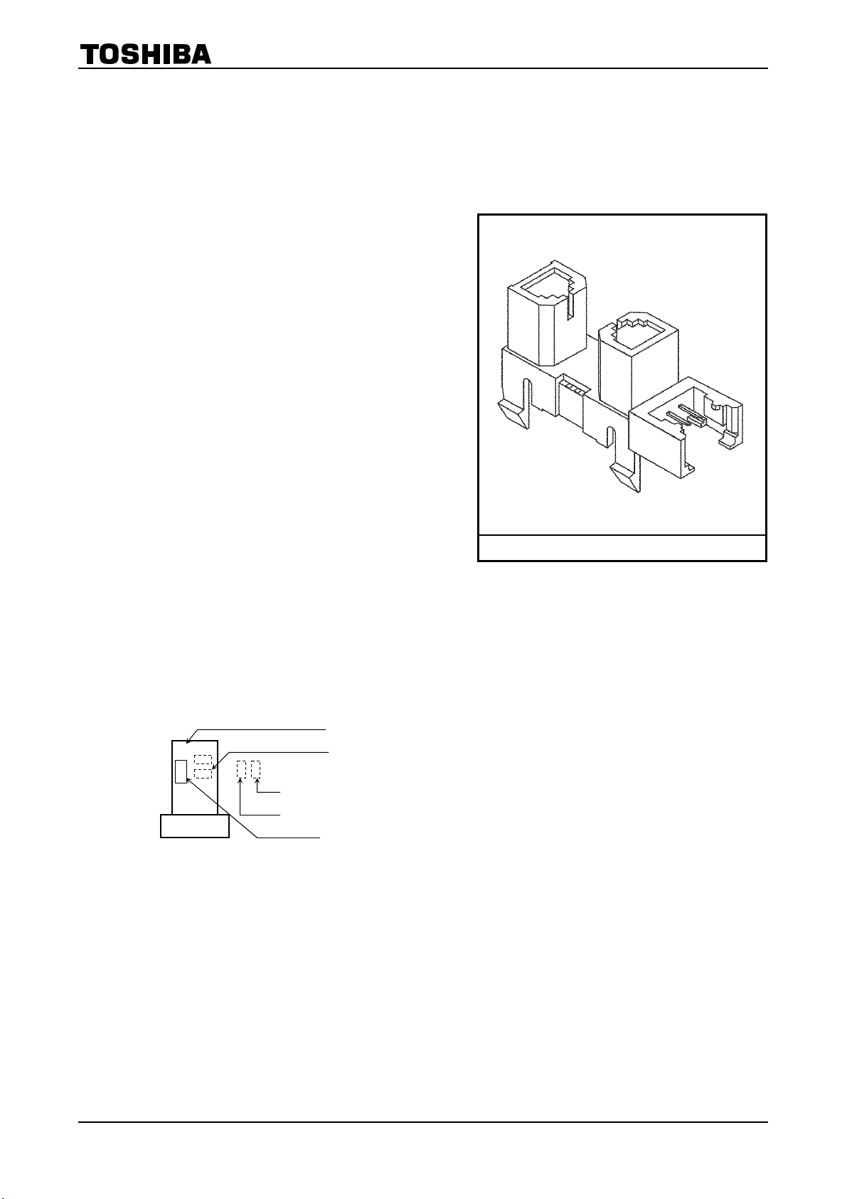
The TLP1243 (C8) is a compact photointerrupter with a
built-in connector that uses a GaAs infrared LED and an Si
phototransistor.
• Small package
Compared to Toshiba’s TLP1241 (C5), the volume and the
mounting area of the TLP1243 (C8) are reduced to
approximately 70% and 75% respectively.
• Three board thicknesses supported: 1.0 mm, 1.2 mm and
1.6 mm
• Gap: 5 mm
• Resolution: Slit width = 0.7 mm
• High-temperature operation: T
• Current transfer ratio: IC/IF = 2.5% (min)
• Mini CT connector (1.5-mm pitch, receptacle
assembly/housing crimp type) made by Tyco Electronics
AMP, Ltd.
• Package and connector material: Polycarbonate (UL94V-2)
• Lead(Pb)-Free
= 95°C (max)
opr
Marking
TOSHIBA 11-15G1
Weight: 0.8 g (typ.)
Connector classification
8
43
Monthly lot number
Product No.
Month of manufacture
(January to December, denoted by the letters A to L respectively)
Year of manufacture (the last digit of the calendar year)
1
2007-10-01

TLP1243(C8)
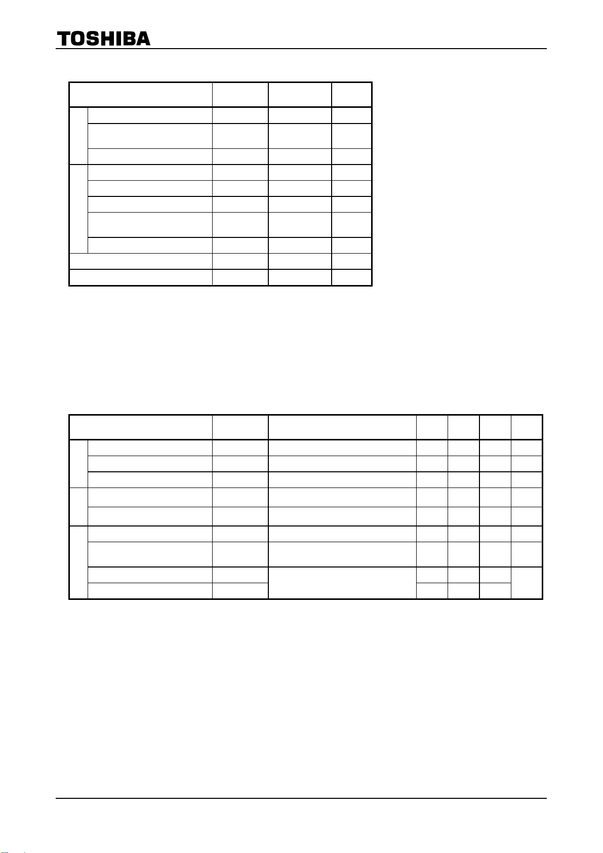
Absolute Maximum Ratings
Characteristics Symbol Rating Unit
Forward current I
Forward current derating
(Ta>25°C)
LED
Reverse voltage VR 5 V
Collector-emitter voltage V
Emitter-collector voltage V
Collector power dissipation PC 75 mW
Collector power dissipation
Detector
derating (Ta>25℃)
Collector current IC 50 mA
Operating temperature range T
Storage temperature range T
(Ta = 25°C)
F
/°C −0.28 mA/°C
ΔI
F
CEO
ECO
/°C −1 mW/°C
ΔP
C
opr
stg
30 mA
35 V
5 V
−30 to 95 °C
−40 to 100 °C
Note: Using continuously under heavy loads (e.g. the application of high temperature/current/voltage and the
significant change in temperature, etc.) may cause this product to decrease in the reliability significantly even
if the operating conditions (i.e. operating temperature/current/voltage, etc.) are within the absolute maximum
ratings.
Please design the appropriate reliability upon reviewing the Toshiba Semiconductor Reliability Handbook
(“Handling Precautions”/“Derating Concept and Methods”) and individual reliability data (i.e. reliability test
report and estimated failure rate, etc).
Optical and Electrical Characteristics
(Ta = 25°C)
Characteristics Symbol Test conditions Min Typ. Max Unit
Forward voltage VF IF = 10 mA 1.00 1.18 1.40 V
Reverse current IR VR = 5 V ⎯ ⎯ 10 μA
LED
Peak emission wavelength λP I
Dark current ID (I
Peak sensitivity wavelength λP ⎯ ⎯ 870 ⎯ nm
Detector
Current transfer ratio IC/IF VCE = 2 V, IF = 10 mA 2.5 ⎯ 100 %
Collector-emitter saturation
voltage
Coupled
Rise time tr ⎯ 15 50
Fall time tf
V
CE (sat)
CEO
= 10 mA ⎯ 940 ⎯ nm
F
) VCE = 24 V, IF = 0 ⎯ 0.001 0.1 μA
IF = 20 mA, IC = 0.25 mA ⎯ 0.1 0.35 V
V
= 5 V, IC = 1 mA, RL = 1 kΩ
CE
⎯ 15 50
μs
2
2007-10-01

TLP1243(C8)
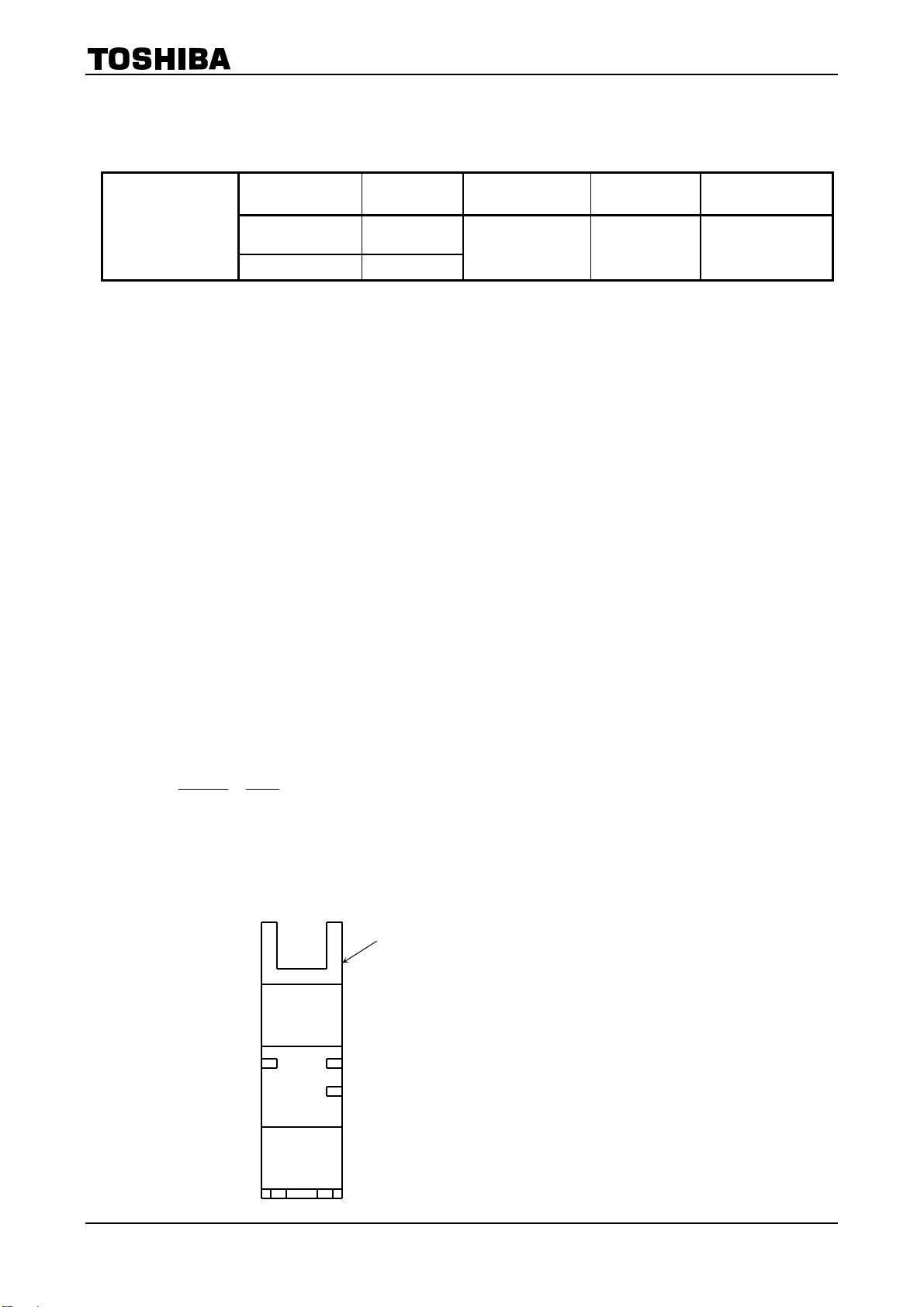
Recommended Connector
Mini CT connector (1.5-mm pitch, receptacle assembly/housing crimp type) made by
Tyco Electronics AMP, Ltd.
External Diameter of
Insulation Coating
Housing-Terminal
En Block Type
Type Model Number Terminal Material AWG Size
Receptacle
assembly
Housing crimp type 353908-3
353293-3
Phosphor bronze AWG26 to 28 0.85 mm to 0.95 mm
Note: For further details of connector characteristics, please contact the relevant connector manufacturer.
Precautions
• Protect the device from ambient light interference. The integrated phototransistor is insensitive to light below
700 nm (e.g., fluorescent light), but is sensitive to light above 700 nm (e.g., incandescent light). If it detects
ambient light, it may cause malfunction. Be sure to make a thorough evaluation of the equipment in which the
device is to be used.
• Care must be taken regarding the environment in which the device is to be installed. Oil or chemicals may
cause the package to melt or crack.
• When attaching the device to the metal board, always hold the body of the device. Do not hold the device by the
connector. Ensure that the board is flat, and not warped or twisted. Attach the device to the metal board at
room temperature.
• Toshiba recommends attaching the device to the smoother side of the board.
• Toshiba recommends testing the attachment strength beforehand by actually attaching a device to the board.
• Do not apply solder to the pins of the device's connector. Make sure that the connector is plugged into the Mini
CT connector or equivalent connector.
• When inserting or removing the Mini CT connector or equivalent connector, always grasp it and its cable firmly
and either plug it straight into or pull it straight out of the device's connector. If the Mini CT connector or
equivalent connector is inserted or removed at an angle, both the device's connector and the Mini CT connector
or equivalent connector may get damaged, resulting in an unreliable connection.
• Conversion efficiency decreases over time due to current flow in the infrared LED. When designing a circuit,
take into account this change in conversion efficiency over time. The ratio of fluctuation in conversion efficiency
to fluctuation in infrared LED optical output is 1:1:
I
I
C/IF (t)
C/IF (0)
P
o (t)
=
P
.
o (0)
• The leadframe of the package is exposed as shown below. Ensure that no conductive material or object (such as
a metal pin) comes into contact with the leads of the leadframe and shorts them together. Care must be taken
when designing a chassis.
Top View
Connector
(1) (2)
(3)
(4) (5)
Leads (1) to (5) of the leadframe shown
on the left must not be shorted together.
3
2007-10-01

TLP1243(C8)
Package Dimensions:
TOSHIBA 11-15G1
Tolerances are listed below unless
otherwise specified.
Dimensions Tolerance
6 mm or less ±0.1
Greater than 6 mm ±0.2
Unit: mm
Weight: 0.8 g (typ.)
Pin Connection
3. Anode
1. Collector
2. Cathode, Emitter
4
2007-10-01

TLP1243(C8)
40
I
F
– Ta
– Ta
P
80
C
(mA)
30
F
60
20
10
Allowable forward current I
0
0 20 40 60 80 100
Ambient temperature Ta (°C)
40
(mW)
C
P
20
Allowable collector power dissipation
0
0 20 40 60 80 100
Ambient temperature Ta (°C)
(mA)
Forward current I
100
50
30
F
10
5
3
Ta = 75°C
IF – VF (typ.)
25 −25 0
50
1
0.9 1.0 1.1 1.2 1.3 1.4
Forward voltage VF (V)
1.5
50
30
(%)
F
/I
C
10
5
3
Current transfer ratio I
1
0.5
1 3 10 5 30 50 100
IC/IF – IF (typ.)
Sample 2
Sample 1
Ta = 25°C
Forward current IF (mA)
: VCE = 2 V
: VCE = 0.4 V
(mA)
C
Collector current I
0.5
0.3
0.1
0.05
0.03
0.01
0.005
10
5
3
1
Sample 2
Forward current IF (mA)
IC – IF (typ.)
Sample 1
Ta = 25°C
: VCE = 2 V
: VCE = 0.4 V
10 30 3 50 5 1
100
6
Ta = 25°C
5
4
(mA)
C
3
2
Collector current I
1
0
0 2 4 6 8 10 12
Collector-emitter voltage VCE (V)
IC –VCE (typ.)
IF = 5 mA
20
15
10
5
2007-10-01

TLP1243(C8)
Relative I
1.2
– Ta (typ.)
C
I
10
(I
) – Ta (typ.)
D
CEO
VCE = 24 V
1.0
0.8
0.6
Relative collector current
0.4
0.2
−40 100 60 20 −20 40 0 80
Ambient temperature Ta (°C)
VCE = 2 V
: IF = 20 mA
: IF = 10 mA
: IF = 5 mA
1
) (μA)
CEO
(I
D
0.1
0.01
Dark current I
0.001
0 20 40 60 100 120 80
Ambient temperature Ta (°C)
V
0.20
0.16
– Ta (typ.)
CE (sat)
IC = 0.25 mA
IF = 20 mA
0.12
(V)
(sat)
0.08
CE
V
Switching Time Test Circuit
I
F
L
R
V
V
CC
OUT
V
I
OUT
F
90%
t
d
t
r
10%
t
f
t
s
0.04
Collector-emitter saturation voltage
0.0
−40 100 60 20 −20 40 0 80
Ambient temperature Ta (°C)
6
2007-10-01

TLP1243(C8)
Switching characteristics
(non-saturated operation) (typ.)
100
Ta = 25°C
30
VCC = 5 V
V
= 1 V
OUT
tr, tf
Switching characteristics
(saturated operation) (typ.)
3000
Ta = 25°C
IF = 20 mA
VCC = 5 V
1000
V
≥ 4.65 V
OUT
tf
10
td
3
Switching time (μs)
ts
300
100
30
Switching time (μs)
ts
tr
1
0.3
0.1 0.3 1 3 10
Load resistance RL (kΩ)
10
td
3
1 3 10 30 100 300
Load resistance RL (kΩ)
Detection position
1.2
1
0.8
0.6
0.4
Relative collector current
0.2
0
−3 −2 −1 0 1 3 4 2
characteristics (1) (typ.)
IF = 10 mA
VCE = 2 V
Ta = 25°C
Shutter
Detection position
d = 0 ± 0.4 mm
Distance d (mm)
Detection position
1.2
0 +
−
d
1
0.8
0.6
0.4
Relative collector current
0.2
0
characteristics (2) (typ.)
IF = 10 mA
VCE = 2 V
Ta = 25°C
Detection position
d = 9.6 mm
Distance d (mm)
Shutter
d
1.2 mm Metal
board thickness
+ 1.9
− 0.9
14 7 8 9 10 11 13 12
7
2007-10-01

TLP1243(C8)
A A
Relative Positioning of Shutter and Device
For normal operation, position the shutter and the device as shown in the figure below. By considering the
device’s detection direction characteristic and switching time, determine the shutter slit width and pitch.
Shutter
Center of sensor
a
’
Metal board
Unit: mm
Thickness of Metal Board a Dimension b Dimension
b
Cross section between A and A'
1.0 11.7 min 8.9 max
1.2 11.5 min 8.7 max
1.6 11.1 min 8.3 max
Recommended Size of Connection Holes
1.0-mm thick metal board 1.2-mm thick metal board 1.6-mm thick metal board
6.65 ± 0.1
15.3 ± 0.1
3.1 ± 0.1 3.1 ± 0.1
6.65 ± 0.1
(Unit: mm)
5.2 ± 0.1
15.3 ± 0.1
5.2 ± 0.1
6.65 ± 0.1
6.4 ± 0.1
15.3 ± 0.1
6.4 ± 0.1
8
2007-10-01

TLP1243(C8)
RESTRICTIONS ON PRODUCT USE
• The information contained herein is subject to change without notice.
• TOSHIBA is continually working to improve the quality and reliability of its products. Nevertheless, semiconductor
devices in general can malfunction or fail due to their inherent electrical sensitivity and vulnerability to physical
stress. It is the responsibility of the buyer, when utilizing TOSHIBA products, to comply with the standards of
safety in making a safe design for the entire system, and to avoid situations in which a malfunction or failure of
such TOSHIBA products could cause loss of human life, bodily injury or damage to property.
In developing your designs, please ensure that TOSHIBA products are used within specified operating ranges as
set forth in the most recent TOSHIBA products specifications. Also, please keep in mind the precautions and
conditions set forth in the “Handling Guide for Semiconductor Devices,” or “TOSHIBA Semiconductor Reliability
Handbook” etc.
• The TOSHIBA products listed in this document are intended for usage in general electronics applications
(computer, personal equipment, office equipment, measuring equipment, industrial robotics, domestic appliances,
etc.).These TOSHIBA products are neither intended nor warranted for usage in equipment that requires
extraordinarily high quality and/or reliability or a malfunction or failure of which may cause loss of human life or
bodily injury (“Unintended Usage”). Unintended Usage include atomic energy control instruments, airplane or
spaceship instruments, transportation instruments, traffic signal instruments, combustion control instruments,
medical instruments, all types of safety devices, etc.. Unintended Usage of TOSHIBA products listed in his
document shall be made at the customer’s own risk.
• The products described in this document shall not be used or embedded to any downstream products of which
manufacture, use and/or sale are prohibited under any applicable laws and regulations.
• The information contained herein is presented only as a guide for the applications of our products. No
responsibility is assumed by TOSHIBA for any infringements of patents or other rights of the third parties which
may result from its use. No license is granted by implication or otherwise under any patents or other rights of
TOSHIBA or the third parties.
20070701-EN
• GaAs(Gallium Arsenide) is used in this product. The dust or vapor is harmful to the human body. Do not break,
cut, crush or dissolve chemically.
• Please contact your sales representative for product-by-product details in this document regarding RoHS
compatibility. Please use these products in this document in compliance with all applicable laws and regulations
that regulate the inclusion or use of controlled substances. Toshiba assumes no liability for damage or losses
occurring as a result of noncompliance with applicable laws and regulations.
9
2007-10-01
 Loading...