

现货库存、技术资料、百科信息、热点资讯,精彩尽在鼎好!
TOSHIBA Photocoupler GaAs Ired & Photo-Transistor
TLP120
Programmable Controllers
AC / DC−Input Module
Telecommunication
The TOSHIBA mini flat coupler TLP120 is a small outline coupler,
suitable for surface mount assembly.
TLP120 consists of a photo transistor, optically coupled to two gallium
arsenide infrared emitting diode connected inverse parallel, and can
operate directly by AC input current.
l Collector−emitter voltage: 80 V (min.)
l Current transfer ratio: 50% (min.)
Rank GB: 100% (min.)
l Isolation voltage: 3750Vrms (min.)
l UL recognized: UL1577, file no. E67349
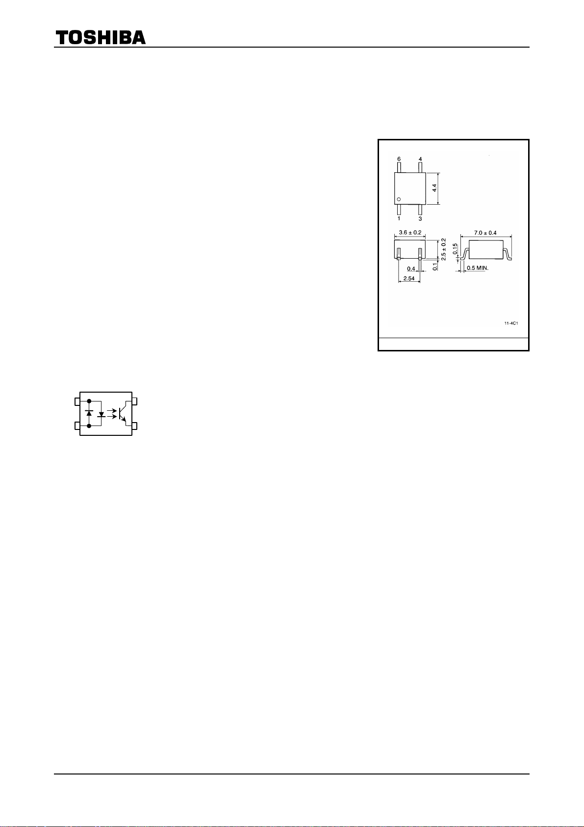
Pin Configurations
(top view)
TLP120
Unit in mm
TOSHIBA 11−4C1
Weight: 0.09 g
1
3
1: Anode
Cathode
3: Cathode
Anode
4: Emitter
6: Collector
6
4
1
2002-09-25

TLP120
Maximum Ratings
Characteristic Symbol Rating Unit
Forward current I
Forward current derating ∆IF / °C -0.7 (Ta ≥ 53°C) mA / °C
LED
Pulse forward current IFP 1 (100µs pulse, 100pps) A
Junction temperature Tj 125 °C
Collector-emitter voltage V
Emitter-collector voltage V
Collector current IC 50 mA
Collector power dissipation PC 150 mW
Detector
Collector power dissipation
derating (Ta ≥ 25°C)
Junction temperature Tj 125 °C
Storage temperature range T
Operating temperature range T
Lead soldering temperature T
Total package power dissipation PT 200 mW
Total package power dissipation
derating (Ta ≥25°C)
Isolation voltage (Note 1) BVS 3750 (AC, 1min., R.H. ≤ 60%) Vrms
(Ta = 25°C)
50 mA
F(RMS)
80 V
CEO
7 V
ECO
∆P
/ °C -1.5 mW / °C
C
-55~125 °C
stg
-55~100 °C
opr
260 (10s) °C
sol
∆P
/ °C -2.0 mW / °C
T
(Note 1) Device considered a two terminal device: Pins1, 3 shorted together and pins 4, 6 shorted together.
Recommended Operating Conditions
Characteristic Symbol Min. Typ. Max. Unit
Supply voltage VCC ― 5 48 V
Forward current I
Collector current IC ― 1 10 mA
Operating temperature T
― 16 20 mA
F(RMS)
-25 ― 85 °C
opr
2
2002-09-25

TLP120
Individual Electrical Characteristics
Characteristic Symbol Test Condition Min. Typ. Max. Unit
Forward voltage VF IF = ±10 mA 1.0 1.15 1.3 V
LED
Capacitance CT V = 0, f = 1 MHz — 60 — pF
Collector-emitter
breakdown voltage
Emitter-collector
breakdown voltage
Detector
Collector dark current I
Capacitance
(collector to emitter)
Coupled Electrical Characteristics
Characteristic Symbol Test Condition MIn. Typ. Max. Unit
Current transfer ratio IC / I
Saturated CTR IC / I
Collector-emitter
saturation voltage
Off-state collector current I
CTR symmetry I
Isolation Characteristics
(Ta = 25°C)
V
(BR)CEO
V
(BR)ECO
CEO
C
CE
(Ta = 25°C)
F (sat)
V
CE (sat)
C(off)
C (ratio)
(Ta = 25°C)
IC = 0.5 mA 80 — — V
IE = 0.1 mA 7 — — V
VCE = 48 V — 10 100 nA
V
CE
V = 0, f = 1 MHz — 10 — pF
= 48 V, Ta = 85°C — 2 50 µA
IF = ±5 mA, VCE = 5 V
F
IF = ±1 mA, VCE = 0.4 V
IC = 2.4 mA, IF = ±8 mA — — 0.4
IC = 0.2 mA, IF = ±1 mA
VF = ± 0.7V, VCE = 48 V — 1 10 µA
I
(IF = -5mA) / IC (IF = 5mA) 0.33 1 3 —
C
Rank GB
Rank GB
Rank GB
50 — 600
100 — 600
— 60 —
30 — —
— 0.2 —
— — 0.4
%
%
V
Characteristic Symbol Test Condition Min. Typ. Max. Unit
Capacitance
(input to output)
Isolation resistance R
Isolation voltage BV
C
VS = 0, f = 1 MHz — 0.8 — pF
S
10
14
VS = 500 V, R.H. ≤ 60% 5×10
S
AC, 1 minute 3750 — —
AC, 1 second, in oil — 10000 —
S
DC, 1 minute, in oil — 10000 — V
10
— Ω
V
rms
dc
3
2002-09-25
TLP120
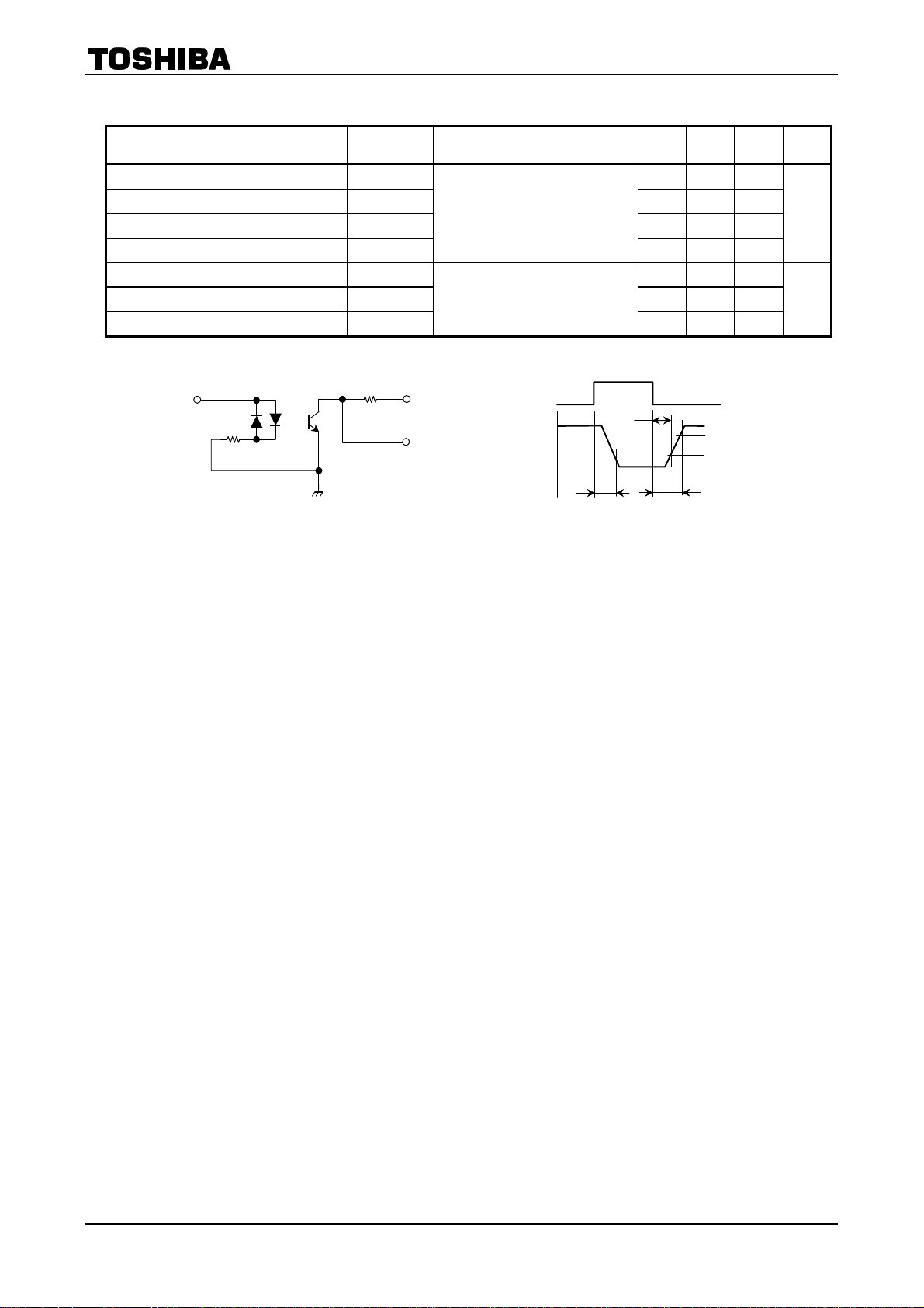
Switching Characteristics
Characteristic Symbol Test Condition Min. Typ. Max. Unit
Rise time t
Fall time t
Turn-on time t
Turn-off time t
Turn-on time t
Storage time t
Turn-off time t
(Ta = 25°C)
Fig. 1 Switching time test circuit
I
F
— 2 —
r
— 3 —
f
VCC = 10 V, IC = 2 mA
R
= 100Ω
— 3 —
on
off
ON
— 25 —
s
OFF
R
L
L
— 3 —
— 2 —
RL = 1.9 kΩ (Fig.1)
V
= 5 V, IF = ±16 mA
CC
I
V
CC
V
CE
F
V
CE
t
ON
— 40 —
t
S
t
OFF
V
CC
4.5V
0.5V
µs
µs
4
2002-09-25

TLP120
100
I
– Ta
F
200
P
– Ta
C
(mW)
C
160
120
80
60
dissipation P
Allowable collector power
Forward current IF (mA)
80
40
100
0.5
0.3
0
- 20
50
30
10
0 20 40 60 80
Ambient temperature Ta (°C)
- VF
I
F
Ta = 25°C
5
3
1
100 120
40
(mA)
F
I
20
Allowable forward current
0
-20 100
60 120 40 80 20 0
Ambient temperature Ta (°C)
– DR
I
FP
3000
1000
500
300
(mA)
100
FP
I
50
Pulse forward current
30
Pulse wi dth ≤ 100µs
Ta = 25°C
Forward voltage temperature
10
3
-3.2
-2.8
-2.4
-2.0
/ΔTa(mV/ ℃)
F
-1.6
-1.2
-0.8
coefficient ΔV
-0.4
0.1 0.3 3 5 50 1
10-3
-2
3 3 3
Duty cycle ratio D
/ ΔTa – IF
ΔV
F
Forward current I
0.1
0.4
0.8 1.2 1.6
100 10-1 10
R
1000
500
300
(mA)
100
FP
50
30
10
5
3
Pulse forward current I
1
(mA)
F
30 10 0.5
1.0
Forward voltage V
- VFP
I
FP
Pulse width ≤ 10µs
Repetitive
Frequency = 100Hz
Ta = 25°C
1.0
Pulse forward voltage V
(V)
F
FP
(V)
1.8 1.4
3.0 2.6 2.2 1.8 1.4 0.6
5
2002-09-25
TLP120
– VCE
I
50
40
(mA)
C
30
20
Collector current I
10
C
50mA
30mA
20mA
15mA
10mA
Ta = 25°C
IF = 5mA
P
C(MAX)
30
Ta = 2 5° C
(mA)
20
C
10
Collector current I
- VCE
I
C
IF = 50mA
40mA
30mA
20mA
10mA
5mA
2mA
0
0
100
50
30
10
C (mA)
5
3
1
0.5
Collector current I
0.3
0.3
2 4 6 8 10
Collecor-emitter voltage V
Ta = 25°C
SAMPLE A
SAMPLE B
3
1
10 0.5
5
(V)
CE
VCE = 10V
VCE = 5V
VCE = 0.4V
30
50
100
Forward current IF (mA)
0
0 0.2
0.4
0.6
0.8
1.0
Collector-emitter voltage VCE (V)
- Ta
I
1
10
0
10
CEO
(µA)
CEO
-1
10
-2
10
VCE = 48V
24V
10V
5V
Collector dark current I
-3
10
/ IF - IF
I
1000
VCE = 10V
500
(%)
F
300
/ I
C
VCE = 5V
VCE = 0.4V
SAMPLE A
C
Ta = 25°C
-4
10
40
20 0
80 60
120 100
Ambient temperature Ta (°C)
100
SAMPLE B
50
Current transfer ratio I
30
0.3
100 50 30 10 5 3 0.5 1
Forward current IF (mA)
6
2002-09-25
TLP120
0.24
0.20
V
CE(sat)
– Ta
IF = 5mA
IC = 1mA
100
50
- Ta
I
C
IF = 25mA
VCE = 5V
(V)
0.16
CE(sat)
0.12
0.08
voltage V
Collector-emitter saturation
0.04
1000
500
300
0
Ta = 25°C
IF = 16mA
VCC = 5V
0
-20 -40
20 40 60 80 100
Ambient temperature Ta (
Switching Time - R
t
OFF
°C)
L
30
10
(mA)
C
5
3
1
Collector current I
0.5
0.3
0.1
-20
0
20
40
10
5
1
0.5
80 60
100
Ambient temperature Ta (°C)
100
50
30
ts
Switching time (µs)
10
5
3
tON
1
Load resistance R
(kΩ)
L
100 50 30 10 5 3 1
7
2002-09-25

TLP120
RESTRICTIONS ON PRODUCT USE
· TOSHIBA is continually working to improve the quality and reliability of its products. Nevertheless, semiconductor
devices in general can malfunction or fail due to their inherent electrical sensitivity and vulnerability to physical
stress. It is the responsibility of the buyer, when utilizing TOSHIBA products, to comply with the standards of
safety in making a safe design for the entire system, and to avoid situations in which a malfunction or failure of
such TOSHIBA products could cause loss of human life, bodily injury or damage to property.
In developing your designs, please ensure that TOSHIBA products are used within specified operating ranges as
set forth in the most recent TOSHIBA products specifications. Also, please keep in mind the precautions and
conditions set forth in the “Handling Guide for Semiconductor Devices,” or “TOSHIBA Semiconductor Reliability
Handbook” etc..
· The TOSHIBA products listed in this document are intended for usage in general electronics applications
(computer, personal equipment, office equipment, measuring equipment, industrial robotics, domestic appliances,
etc.). These TOSHIBA products are neither intended nor warranted for usage in equipment that requires
extraordinarily high quality and/or reliability or a malfunction or failure of which may cause loss of human life or
bodily injury (“Unintended Usage”). Unintended Usage include atomic energy control instruments, airplane or
spaceship instruments, transportation instruments, traffic signal instruments, combustion control instruments,
medical instruments, all types of safety devices, etc.. Unintended Usage of TOSHIBA products listed in this
document shall be made at the customer’s own risk.
· Gallium arsenide (GaAs) is a substance used in the products described in this document. GaAs dust and fumes
are toxic. Do not break, cut or pulverize the product, or use chemicals to dissolve them. When disposing of the
products, follow the appropriate regulations. Do not dispose of the products with other industrial waste or with
domestic garbage.
· The products described in this document are subject to the foreign exchange and foreign trade laws.
000707EBC
· The information contained herein is presented only as a guide for the applications of our products. No
responsibility is assumed by TOSHIBA CORPORATION for any infringements of intellectual property or other
rights of the third parties which may result from its use. No license is granted by implication or otherwise under
any intellectual property or other rights of TOSHIBA CORPORATION or others.
· The information contained herein is subject to change without notice.
8
2002-09-25
 Loading...