

现货库存、技术资料、百科信息、热点资讯,精彩尽在鼎好!
TOSHIBA PHOTOCOUPLER GaAℓAs LED & PHOTO-IC
TLP116
PDP(Plasma Display Panel)
High Speed Interface
FA(Factory Automation)
The Toshiba TLP116 consists of a GaAℓAs light-emitting diode and an
integrated high-gain, high-speed photodetector.
z Inverter logic (totempole output)
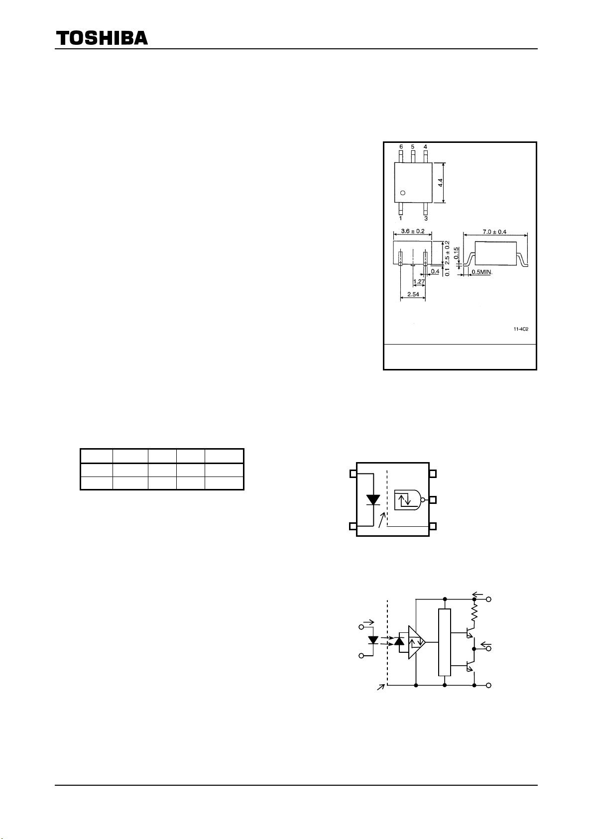
z Package type : MFSOP6
z Guaranteed performance over temperature : -40~100°C
z Power supply voltage : 4.5~5.5V
TLP116
Unit in mm
z Input thresholds current : I
z Propagation delay time (tpHL/tpLH) : 60ns(Max.)
z Switching speed : 20MBd(TYP.)
z Common mode transient immunity : 10kV/us
z Isolation voltage : 3750Vrms
z UL Recognized
: UL1577,File No.E67349
=5mA(Max.)
FHL
TOSHIBA 11-4C2
Weight: 0.09 g(Typ.)
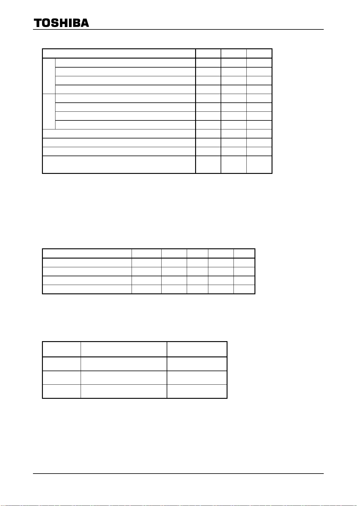
Truth Table Pin Configuration (Top View)
Input LED Tr1 Tr2 Output
H
ON OFF ON
OFF ON OFF H
L
L
1
3
SHIELD
VCC
GND
1:ANODE
6
3:CATHODE
5
4:GND
5:VO
4
6:VCC
I
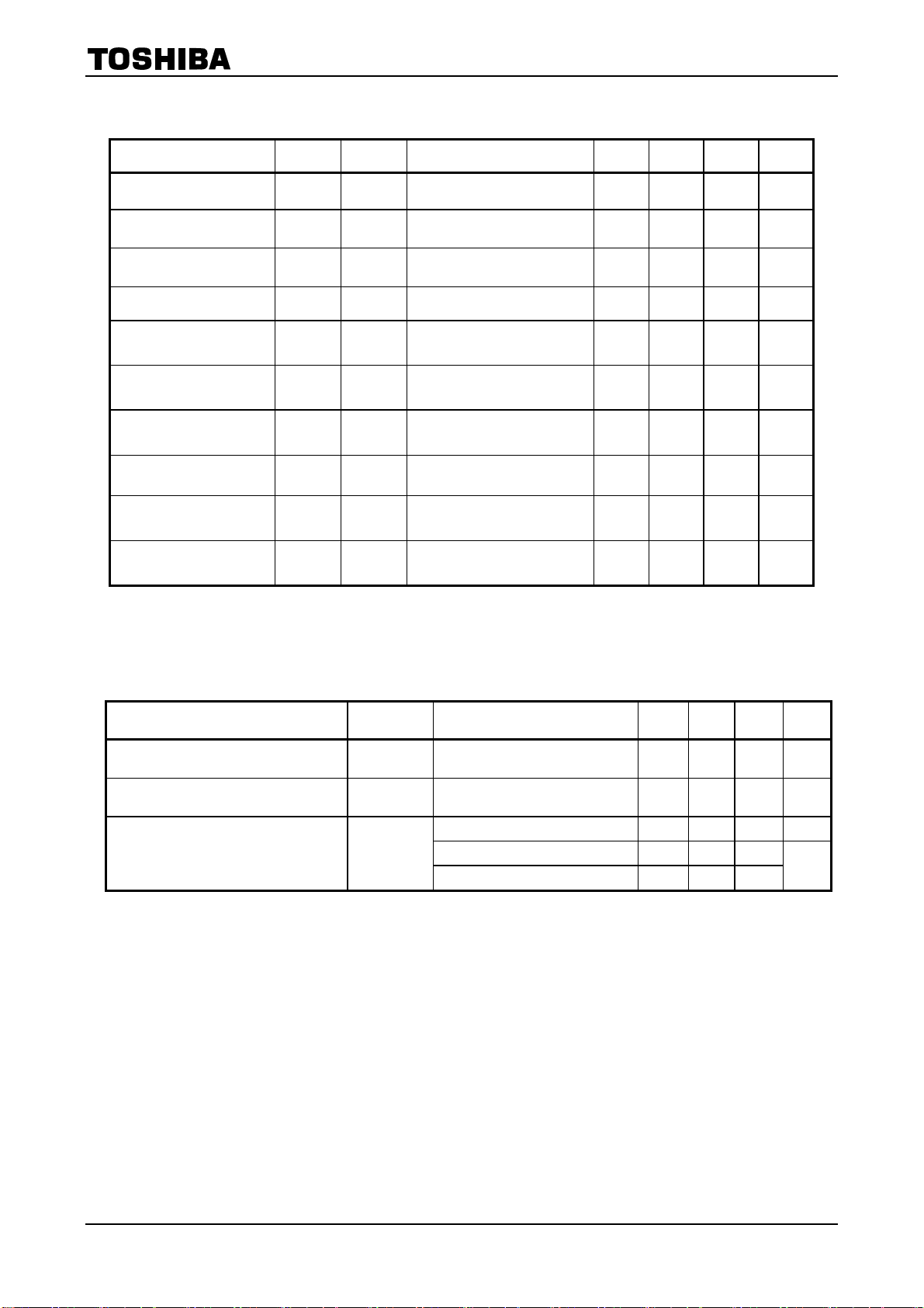
Schematic
1+
3-
I
F
Tr1
Tr2
CC
V
CC
6
I
O
V
O
5
SHIELD
0.1uF bypass capacitor must be
connected between pins 6 and 4
4
2007-10-01 1
GND
Absolute Maximum Ratings (Ta=25°C)
Characteristic Symbol Rating Unit
Forward current IF 20 mA
Forward current derating (Ta≥85°C) ΔIF/ΔTa -0 . 5 mA / °C
LED
Peak transient forward current (Note1) I
Reverse voltage VR 5 V
Output current IO 10 mA
Output voltage VO 6 V
Supply voltage VCC 6 V
DETECTOR
Output power dissipation PO 40 mW
Operating temperature range Topr -40~100 °C
Storage temperature range Tstg -55~125 °C
Lead solder temperature(10s) Tsol 260 °C
Isolation voltage
(AC,1min.,R.H.≤60%,Ta=25°C) (Note2)
1 A
FPT
BVs 3750 Vrms
Note: Using continuously under heavy loads (e.g. the application of high temperature/current/voltage and the
significant change in temperature, etc.) may cause this product to decrease in the reliability significantly even
if the operating conditions (i.e. operating temperature/current/voltage, etc.) are within the absolute maximum
ratings and the operating ranges.
Please design the appropriate reliability upon reviewing the Toshiba Semiconductor Reliability Handbook
(“Handling Precautions”/“Derating Concept and Methods”) and individual reliability data (i.e. reliability test
report and estimated failure rate, etc).
Recommended Operating Conditions
TLP116
Characteristic Symbol Min Typ. Max Unit
Input current , ON I
Input voltage , OFF V
Supply voltage (Note3) VCC 4.5 5.0 5.5 V
Operating temperature Topr -40 — 100 °C
8
F(ON)
F(OFF)
0
—
—
18 mA
0.8 V
Note: Recommended operating conditions are given as a design guideline to obtain expected performance of the
device. Additionally, each item is an independent guideline respectively. In developing designs using this
product, please confirm specified characteristics shown in this document.
Correlation between Input current , switching speed and drive circuit
(reference information).
Input current
(IF)
12mA
8mA
8mA
(Page 4,With Speed up capacitor)
Note1 : Pulse width PW≤1us,300pps.
Note2 : This device is regarded as a two terminal device : pins 1 and 3 are shorted together, as are pins 4,5 and 6.
Note3 : The detector of this product requires a power supply voltage (VCC) of 4.5 V or higher for stable operation.
If the VCC is lower than this value, an ICC may increase, or an output may be unstable.
Be sure to use the product after checking the supply current, and the operation of a power-on/-off.
test Circuit Typical switching speed
1
(Page 4)
1
(Page 4)
2
21 – 23 MBd
18 – 20 MBd
23 – 27 MBd
2007-10-01 2
Electrical Characteristics
(Unless otherwise specified, Ta=-40 to 100°C,VCC=4.5~5.5V )
Characteristic
Symbol
Te st
Circuit
Conditions Min. Typ. Max. Unit
TLP116
Input forward voltage VF
Temperature coefficient
of forward voltage
Input reverse current IR
Input capacitance CT
Logic low output voltage VOL 1
Logic high output voltage VOH 2
Logic low supply current I
Logic high supply current I
Input current logic low
output
Input voltage logic high
output
ΔVF/ΔTa
3 IF=12mA
CCL
4 VF=0V
CCH
I
FHL
V
FLH
*All typical values are at Ta=25°C,V
=5V,IF(ON)=12mA unless otherwise specified
CC
Isolation Characteristics
(Ta = 25°C)
—
IF=10mA ,Ta=25°C — 1.3 1.5 V
—
IF=10mA
—
VR=5V,Ta=25°C
—
V=0,f=1MHz,Ta=25°C
IOL=1.6mA,
IF=12mA,VCC=5V
IOH=-0.02mA,
VF=1.05V,VCC=5V
—
IO=1.6mA,VO<0.4V —
—
IO=-0.02mA,VO>4.0V 0.8
—
-2.0 — mV/°C
— —
— 70
— —
4.0
— —
— —
— —
— 5 mA
— —
10 μA
— pF
0.4 V
V
5.0 mA
5.0 mA
V
Characteristic Symbol Test Conditions Min. Typ. Max. Unit
Capacitance input to output CS V = 0,f = 1MHz (Note 2) ― 0.8 ― pF
12
Isolation resistance R
Isolation voltage BV
R.H. ≤ 60%,VS = 500V
S
(Note 2)
AC,1 minute 3750 ― ― V
AC,1 second,in oil ― 10000 ―
S
DC,1 minute,in oil ― 10000 ―
1×10
14
10
― Ω
Note 4:A ceramic capacitor(0.1 μF) should be connected from pin 6 to pin 4 to stabilize the operation of the high
gain linear amplifier. Failure to provide the bypass may impair the switching property.
The total lead length between capacitor and coupler should not exceed 1 cm.
rms
Vdc
2007-10-01 3

Switching Characteristics
(Unless otherwise specified, Ta=-40 to 100°C,VCC=4.5~5.5V)
Characteristic Symbol
Propagation delay time
to logic high output
Propagation delay time
to logic low output
Propagation delay time
to logic high output
Propagation delay time
to logic low output
Switching time dispersion
between ON and OFF
Output fall time(90-10%) tf
Output rise time(10-90%) tr
tpHL
tpLH
tpHL
tpLH
|tpHL-
tpLH|
Te st
Circuit
5
6
5
Conditions Min. Typ. Max. Unit
IF=0→12mA
IF=12→0mA
V
=0→5V
IN
(IF=0→8mA)
V
=5→0V
IN
(IF=8→0mA)
IF=12mA , R
CL=15pF (Note 5)
IF=0→12mA
IF=12→0mA
(Note 5)
=100Ω,
IN
R
=100Ω
IN
CL=15pF
(Note 5)
R
=470Ω
IN
27pF
C
IN=
CL=15pF
R
=100Ω
IN
CL=15pF
(Note 5)
— —
— —
— —
— —
—
—
—
— 30
15
15
TLP116
60 ns
60 ns
60 ns
60 ns
ns
—
—
ns
ns
Common mode transient
immunity at high Level
output
Common mode transient
immunity at low level
output
*All typical values are at Ta=25°C
Note 5 : CL is approximately 15pF which includes probe and Jig/stray wiring capacitance.
TEST CIRCUIT 1 : V
IF
→
↑
1
3
SHIELD
TEST CIRCUIT 3 : I
IF
→
↑
1
3
SHIELD
CMH
CML
TEST CIRCUIT 2 : V
OL
6
VCC
0.1uF
5
VOL
4
GND
CCL
VCC
GND
V
TEST CIRCUIT 4: I
I
CCL
6
A
5
4
VCM=1000Vp-p,IF=0mA,
Vo(Min)=4V,Ta=25°C
7
VCM=1000Vp-p,IF=12mA,
Vo(Max)=0.4V,Ta=25°C
VCC
IOL
↑
VCC
1
3
SHIELD
1
3
SHIELD
10000
-10000
V
CC
GND
V
CC
GND
— —
— —
OH
6
VOH
↑
V
5
0.1uF
4
CCH
I
CCH
6
A
5
4
V/us
V/us
IOH
VCC
VCC
2007-10-01 4

r
TEST CIRCUIT 5 : tpHL , tpLH
TLP116
IF=12mA(P.G)
(f=5MHz , duty=50%)
INPUT
MONITORING
NODE
CL=15pF
RIN=100Ω
SHIELD
CL is capacitance of the probe and JIG.
(P.G) : Pulse Generator
TEST CIRCUIT 6 : tpHL , tpLH
VIN=5V(P.G)
(f=5MHz , duty=50%)
INPUT MONITORING NODE
CL=15pF
CIN=27pF
RIN=470Ω
SHIELD
CL is capacitance of the probe and JIG.
(P.G) : Pulse Generator
VCC
GND
VCC
GND
0.1uF
0.1uF
Vo
MONITORING
NODE
CL=15pF
Vo
MONITORING
NODE
CL=15pF
50%
IF
VCC
VO
tf
1.5V
tpHL
tpLH
tr
10%
90%
VOH
VOL
50%
IF
V
CC
VO
1.5V
tf
tpHL
tpLH
tr
10%
90%
VOH
VOL
TEST CIRCUIT 7 : Common-Mode Transient Immunity Test Circuit
SW
A
IF
→
B
1
3
SHIELD
V
C
M
VCC
GND
6
0.1uF
5
4
V
O
V
CC
・SW B : IF=0mA
・SW A : IF=5mA
CM
H
10%
=
90%
t
1000V
tr
4V
)(800
V
)(
s
μ
CM
tf
CM
H
0.4V
CML
)(800
V
=
L
)(
s
μ
t
f
2007-10-01 5

100
(mA)
F
10
100°C
IF-V
25°C
TLP116
F
-40°C
/∆Ta (m V / °C )
F
-3
-2.5
-2
-1.5
∆ VF/ ∆ Ta- I
F
1
Forward Current I
0.1
0.8 1 1.2 1.4 1.6 1.8
1
0.8
OL(V)
Forward Voltage VF(V)
VOL-Ta
IOL=1.6mA , IF=12mA,
VCC=5V
0.6
0.4
0.2
Logic Low Output Voltage V
0
-40-20 0 20406080100
Ambient Temperature Ta(℃)
Coefficient ∆V
6
5
4
3
2
1
Logic High Output Voltage VOH(V)
0
-1
-0.5
0
0.1 1 10 100
Forward Current IF (mA)
VOH-Ta
IOH=-0.02mA , VF=1.05V
VCC=5V
-40-20 0 20406080100
Ambient Temperature Ta(℃)
I
10
IF=12mA
VCC=5.5V
8
(mA)
CCL
CCL
-Ta
6
4
2
Logic low supply current I
0
-40-20 0 20406080100
*: The above graphs show typical characteristics.
Ambient Temperature Ta(℃)
10
(mA)
8
CCH
6
4
2
0
Logic High Supply Current I
-40-20 0 20406080100
I
-Ta
CCH
VF=0V
VCC=5.5V
Ambient Temperature Ta(℃)
2007-10-01 6

TLP116
t
pHL,tpLH
-Ta
60
50
(ns)
PHL
, t
40
PLH
30
20
10
Propagation delay time t
0
-40-200 20406080100
Ambient Temperature Ta(℃)
Test Circuit 5
IF=12mA,RIN=100Ω,
CL=15pF,VCC=5.5V
t
pHL,tpLH-IF
70
60
(ns)
PHL
50
, t
PLH
tpHL
40
30
tpLH
20
10
Propagation delay time t
0 5 10 15 20
Forward Current IF (mA)
Test Circuit 5
RIN=100Ω , CL=15pF
VCC=5.5V
tpHL
tpLH
60
50
(ns)
PHL
, t
40
PLH
30
20
10
Propagation delay time t
0
-40-200 20406080100
60
50
(ns)
PHL
, t
40
PLH
30
20
10
Propagation delay time t
0
4.5 5 5.5
t
pHL,tpLH
Ambient Temperature Ta(℃)
t
pHL,tpLH-VCC
Supply Voltage VCC (V)
-Ta
Test Circuit 6
VIN=5V,RIN=470Ω
C
27pF,CL=15pF,VCC=5.5V
IN=
Test Circuit 5
IF=12mA , RIN=100Ω
CL=15pF , Ta=25°C
tpHL
tpLH
tpHL
tpLH
30
25
|tpHL-tpLH|-Ta
Test Circuit 5
Test Circuit 6
20
15
10
5
between ON and OFF(ns)
Switching Time Dispersion
0
-40-200 20406080100
Ambient Temperature Ta(℃)
*: The above graphs show typical characteristics.
5
IO=1.6mA
VO<0.4V
4
(mA)
FLH
3
2
1
Threshold input current I
0
-40 -20 0 20 40 60 80 100
I
-Ta
FLH
Ambient Temperature Ta(℃)
2007-10-01 7

TLP116
RESTRICTIONS ON PRODUCT USE
• The information contained herein is subject to change without notice.
• TOSHIBA is continually working to improve the quality and reliability of its products. Nevertheless, semiconductor
devices in general can malfunction or fail due to their inherent electrical sensitivity and vulnerability to physical
stress. It is the responsibility of the buyer, when utilizing TOSHIBA products, to comply with the standards of
safety in making a safe design for the entire system, and to avoid situations in which a malfunction or failure of
such TOSHIBA products could cause loss of human life, bodily injury or damage to property.
In developing your designs, please ensure that TOSHIBA products are used within specified operating ranges as
set forth in the most recent TOSHIBA products specifications. Also, please keep in mind the precautions and
conditions set forth in the “Handling Guide for Semiconductor Devices,” or “TOSHIBA Semiconductor Reliability
Handbook” etc.
• The TOSHIBA products listed in this document are intended for usage in general electronics applications
(computer, personal equipment, office equipment, measuring equipment, industrial robotics, domestic appliances,
etc.).These TOSHIBA products are neither intended nor warranted for usage in equipment that requires
extraordinarily high quality and/or reliability or a malfunction or failure of which may cause loss of human life or
bodily injury (“Unintended Usage”). Unintended Usage include atomic energy control instruments, airplane or
spaceship instruments, transportation instruments, traffic signal instruments, combustion control instruments,
medical instruments, all types of safety devices, etc.. Unintended Usage of TOSHIBA products listed in his
document shall be made at the customer’s own risk.
• The products described in this document shall not be used or embedded to any downstream products of which
manufacture, use and/or sale are prohibited under any applicable laws and regulations.
• The information contained herein is presented only as a guide for the applications of our products. No
responsibility is assumed by TOSHIBA for any infringements of patents or other rights of the third parties which
may result from its use. No license is granted by implication or otherwise under any patents or other rights of
TOSHIBA or the third parties.
20070701-EN
• GaAs(Gallium Arsenide) is used in this product. The dust or vapor is harmful to the human body. Do not break,
cut, crush or dissolve chemically.
• Please contact your sales representative for product-by-product details in this document regarding RoHS
compatibility. Please use these products in this document in compliance with all applicable laws and regulations
that regulate the inclusion or use of controlled substances. Toshiba assumes no liability for damage or losses
occurring as a result of noncompliance with applicable laws and regulations.
2007-10-01 8
 Loading...