

现货库存、技术资料、百科信息、热点资讯,精彩尽在鼎好!
TOSHIBA Photocoupler GaAℓAs Ired + Photo−IC
TENTATIVE
TLP114A(IGM)
Transistor Invertor
Inverter For Air Conditioner
Line Receiver
Ipm Interfaces
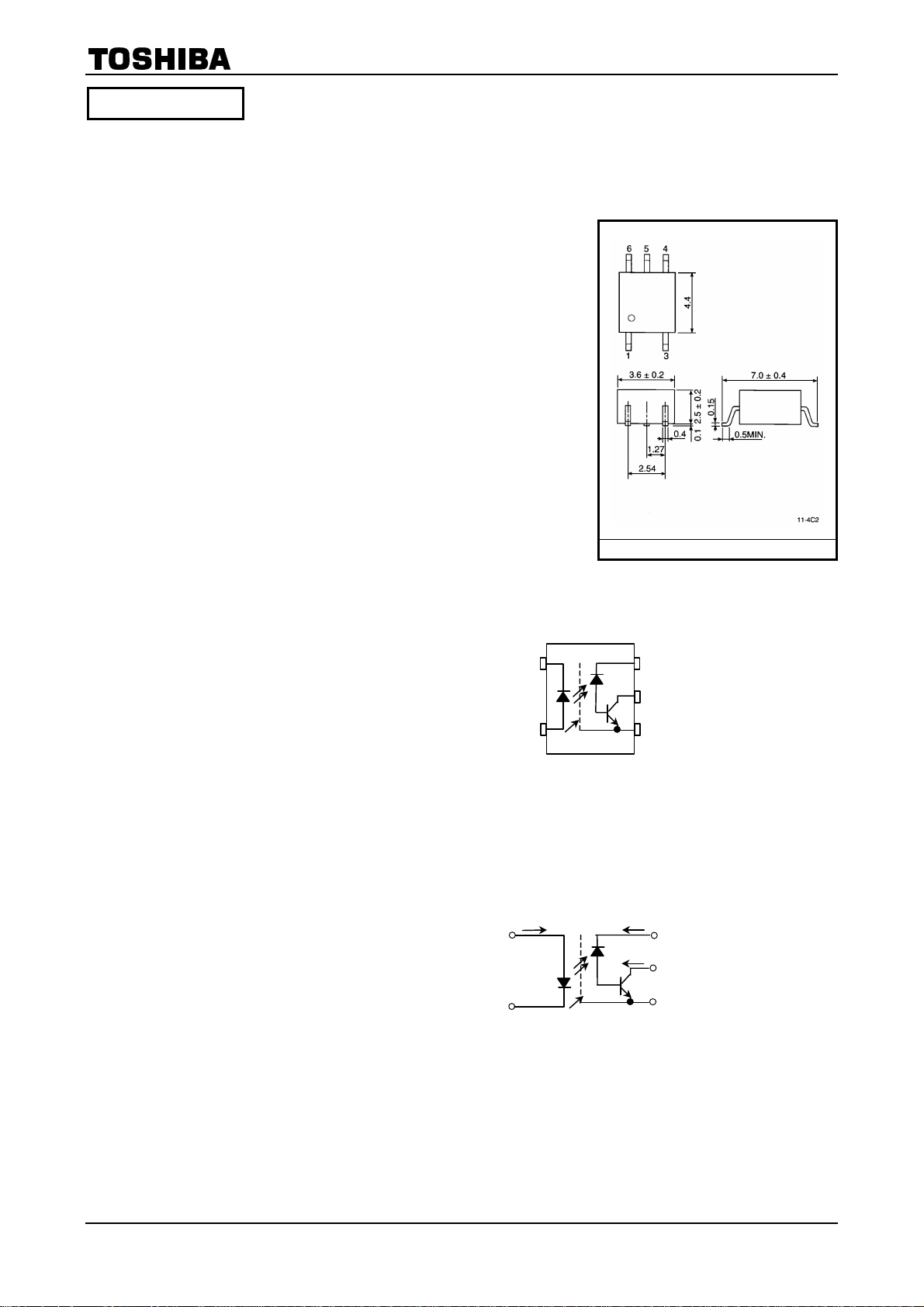
The TOSHIBA mini flat coupler TLP114A is a small outline coupler,
suitable for surface mount assembly.
TLP114A consists of a high output power GaAℓAs light emitting diode,
optically coupled to a high speed detector of one chip photo
diode−transistor.
TLP114A(IGM) has no internal base connection, and a faraday shield
integrated on the photodetector chip provides an effective common
mode noise transient immunity.
TLP114A(IGM) guarantees minimum and maximum of propagation
delay time, switching time dispersion, and high common mode
transient immunity. There for TLP114A(IGM) is suitable for isolation
interface between IPM(intelligent power module) and control IC
circuits in motor control application.
l Isolation voltage: 3750V
l Common mode transient immunity
: ±10kV/µs(min.)
@VCM=1500V
l Switching time: t
=0.8µs(max.)
@IF=10mA, VCC=15V,
R
l Switching time dispersion: 0.7µs(max.)
(|t
pLH−tpHL
l TTL compatible
l UL recognized: UL1577, file no.E67349
pHL, tpLH
=20kΩ, Ta=25°C
L
|)
(min.)
rms
=0.1µs(min.)
Pin Configuration
1
3
SHIELD
1 : Anode
3 : Cathode
4 : Emitter (GND)
5 : Collector (Output)
6 : V
CC
Schematic
TLP114A(IGM)
TOSHIBA 11−4C2
Weight: 0.09g
(top vi ew)
6
5
4
Unit in mm
IF
1
V
F
3
Shield
1
I
IO
CC
6
5
4
VCC
V
O
GND
2002-09-25
TLP114A(IGM)
Maximum Ratings
(Ta = 25°C)
Characteristic Symbol Rating Unit
Forward current (Note 1) I
Pulse forward current (Note 2) I
LED
Peak transient forward current (Note 3) I
Reverse voltage V
Output current I
Peak output current I
Output voltage V
Detector
Supply voltage V
Output power dissipation (Note 4) P
Operating temperature range T
Storage temperature range T
Lead soldering temperature(10s) T
Isolation voltage(AC, 1min., R.H.≤60%, Ta=25°C) (Note 5) BV
(Note 1): Derate 0.36mA above 70°C.
(Note 2): 50% duty cycle, 1ms pulse width.
F
FP
FPT
O
OP
CC
opr
stg
sol
R
O
O
S
20 mA
40 mA
1 A
5 V
8 mA
16 mA
-0.5~20 V
-0.5~30 V
100 mW
-55~100
-55~125
260
3750 Vrms
°C
°C
°C
Derate 0.72mA / °C above 70°C.
(Note 3): Pulse width PW ≤ 1µs, 300pps.
(Note 4): Derate 1.8mW / °C above 70°C.
(Note 5): Device considerd a two terminal device: pins1, 3 shorted together and pins4, 5, 6
shorted together.
2
2002-09-25

TLP114A(IGM)
Electrical Characteristics
Characteristic Symbol Test Condition Min. Typ. Max. Unit
Forward voltage V
Forward voltage
temperature coefficient
Reverse current I
LED
Capacitance between
terminal
High level output current
High level supply
Detector
current
Supply voltage V
Output voltage V
(Ta = 25°C)
∆V
F
CT V
I
OH(1)
I
OH(2)
I
OH
I
CCH
CC
IF=16mA 1.22 1.42 1.72 V
F
/ ∆Ta IF=16mA
VR=3V
R
=0, f=1MHz
F
IF=0mA, VCC=VO=5.5V
IF=0mA, VCC=30V
V
=20V
O
IF=0mA, VCC=30V
V
=20V, Ta=70°C
O
IF=0mA, VCC=30V
ICC=0.01mA 30
IO=0.5mA 20
O
―
―
―
―
-2 ― mV / °C
― 10 µA
30 ― pF
3 500 nA
― ―
― ―
0.01 1 µA
―
― ―
― ―
5
µA
50
V
V
Coupled Electrical Characteristics
(Ta = 25°C)
Characteristic Symbol Test Condition Min. Typ. Max. Unit
Current transfer ratio IO / I
Low level output voltage V
OL
IF=10mA, VCC=4.5V
V
=0.4V
O
F
IF=16mA, VCC=4.5V
V
=0.4V, Ta=-25~100°C
O
IF=10mA, VCC=4.5V
I
=2.4mA
O
25 35 75
15 ― ―
― ― 0.4 V
Isolation Characteristics
Characteristic Symbol Test Condition Min. Typ. Max. Unit
Capacitance input to output CS V=0, f=1MHz (Note 5) ― 0.8 ― pF
Isolation resistance R
Isolation voltage BV
(Ta = 25°C)
R.H.≤60%, VS=500V
S
(Note 5)
5×10
10
14
10
― Ω
AC, 1 minute 3750 ― ―
AC, 1 second, in oil ― 10000 ―
S
DC, 1 minute, in oil ― 10000 ― Vdc
%
Vrms
3
2002-09-25

TLP114A(IGM)
Switching Characteristics
Characteristic Symbol
Propagation delay time
(H→ L)
Propagation delay time
(L→ H)
Switching time
dispersion between on
and off
Common mode
transient immunity at
logic high output
(Note 6)
Common mode
transient immunity at
logic low output
(Note 6)
(Ta = 25°C, V
t
pHL
t
pLH
|t
pLH-tpHL
CM
CM
|
H
L
= 15V)
CC
Test
Cir-
Cuit
IF=0→ 10mA, RL=20kΩ 0.1 0.45 0.8
I
Ta=0~85°C
I
Ta=-25~100°C
1
IF=10→ 0mA, RL=20kΩ ― 0.15 0.7
IF=10→ 0mA, RL=20kΩ
Ta=0~85°C
IF=10→ 0mA, RL=20kΩ
Ta=-25~100°C
IF=0mA
V
RL=20kΩ
2
I
V
RL=20kΩ
Test Condition Min. Typ. Max. Unit
=0→ 10mA, RL=20kΩ
F
=0→ 10mA, RL=20kΩ
F
=1500V
CM
=10mA
F
CM
=1500V
p-p
p-p
(Note 6): CML is the maximum rate of fall of the common mode voltage that can be
0.1 0.45 0.9
0.1 0.45 1.0
― 0.25 0.8
― 0.25 0.9
10000 15000 ― V / µs
-10000
-15000 ― V / µs
µs
µs
sustained with the output voltage in the logic low state (VO<1V).
CMH is the maximum rate of rise of the common mode voltage that can be
sustained with the output voltage in the logic high state (VO<4V).
(Note 7): Maximum electrostatic discharge voltage for any pins: 100V (C=200pF, R=0).
Test Circuit 1: Switching Time Test Circuit
Pulse input
PW = 100µs
Duty ratio = 1/10
monitor
I
F
1
3
100Ω
6
5
4
VCC = 15V
R
L
V
Output
monitor
0.1μF
O
V
I
F
0
t
pLH
15V
1.5V
V
OL
O
1.5V
t
pHL
4
2002-09-25

Test Circuit 2: Common Mode Noise Immunity Test Circuit
IF
1
3
Pulse gen
= 50Ω
Z
O
6
5
4
VCM
VCC = 5V
RL
0.1μF
V
O
Output
monitor
V
CM
V
O
(I
= 0mA)
F
V
O
(IF = 10mA)
t
r
TLP114A(IGM)
1500V
90%
10%
0V
tf
15V
4V
1V
V
OL
CM
)(
H
)(
µsrt
V1200
=
CM
=,
L
)(
V1200
)(
µsft
5
2002-09-25

TLP114A(IGM)
RESTRICTIONS ON PRODUCT USE
· TOSHIBA is continually working to improve the quality and reliability of its products. Nevertheless, semiconductor
devices in general can malfunction or fail due to their inherent electrical sensitivity and vulnerability to physical
stress. It is the responsibility of the buyer, when utilizing TOSHIBA products, to comply with the standards of
safety in making a safe design for the entire system, and to avoid situations in which a malfunction or failure of
such TOSHIBA products could cause loss of human life, bodily injury or damage to property.
In developing your designs, please ensure that TOSHIBA products are used within specified operating ranges as
set forth in the most recent TOSHIBA products specifications. Also, please keep in mind the precautions and
conditions set forth in the “Handling Guide for Semiconductor Devices,” or “TOSHIBA Semiconductor Reliability
Handbook” etc..
· The TOSHIBA products listed in this document are intended for usage in general electronics applications
(computer, personal equipment, office equipment, measuring equipment, industrial robotics, domestic appliances,
etc.). These TOSHIBA products are neither intended nor warranted for usage in equipment that requires
extraordinarily high quality and/or reliability or a malfunction or failure of which may cause loss of human life or
bodily injury (“Unintended Usage”). Unintended Usage include atomic energy control instruments, airplane or
spaceship instruments, transportation instruments, traffic signal instruments, combustion control instruments,
medical instruments, all types of safety devices, etc.. Unintended Usage of TOSHIBA products listed in this
document shall be made at the customer’s own risk.
· Gallium arsenide (GaAs) is a substance used in the products described in this document. GaAs dust and fumes
are toxic. Do not break, cut or pulverize the product, or use chemicals to dissolve them. When disposing of the
products, follow the appropriate regulations. Do not dispose of the products with other industrial waste or with
domestic garbage.
· The products described in this document are subject to the foreign exchange and foreign trade laws.
000707EBC
· The information contained herein is presented only as a guide for the applications of our products. No
responsibility is assumed by TOSHIBA CORPORATION for any infringements of intellectual property or other
rights of the third parties which may result from its use. No license is granted by implication or otherwise under
any intellectual property or other rights of TOSHIBA CORPORATION or others.
· The information contained herein is subject to change without notice.
6
2002-09-25
 Loading...