


现货库存、技术资料、百科信息、热点资讯,精彩尽在鼎好!
TOSHIBA Photocoupler GaAℓAs Ired & Photo−IC
TLP114A
Digital Logic Isolation.
Line Receiver.
Power Supply Control Feedback Control.
Switching Power Supply.
Transistor Inverter.
The TOSHIBA mini flat coupler TLP114A is a small outline coupler,
suitable for surface mount assembly.
TLP114A consists of a high output power GaAℓAs light emitting diode,
optically coupled to a high speed detector of one chip
photodiode-transistor.
• Isolation voltage: 3750 Vrms (min.)
• Switching speed: t
(R
• TTL compatible
• UL recognized: UL1577, file no. E67349
= 1.9 kΩ)
L
p
HL
= 0.8μs, t
= 0.8μs (max.)
LH
p
TLP114A
Unit in mm
TOSHIBA 11−4C2
Weight: 0.09g
Pin Configuration (top view)
6
1
3
SHIELD
1 : ANODE
3 : CATHODE
4 : EMITTER (GND)
5
5 : COLLECTOR (OUTPUT).
6 : V
4
CC
Schematic
IF
1
V
F
3
SHIELD
ICC
I
O
VCC
6
V
O
5
GND
4
2007-10-01 1
TLP114A
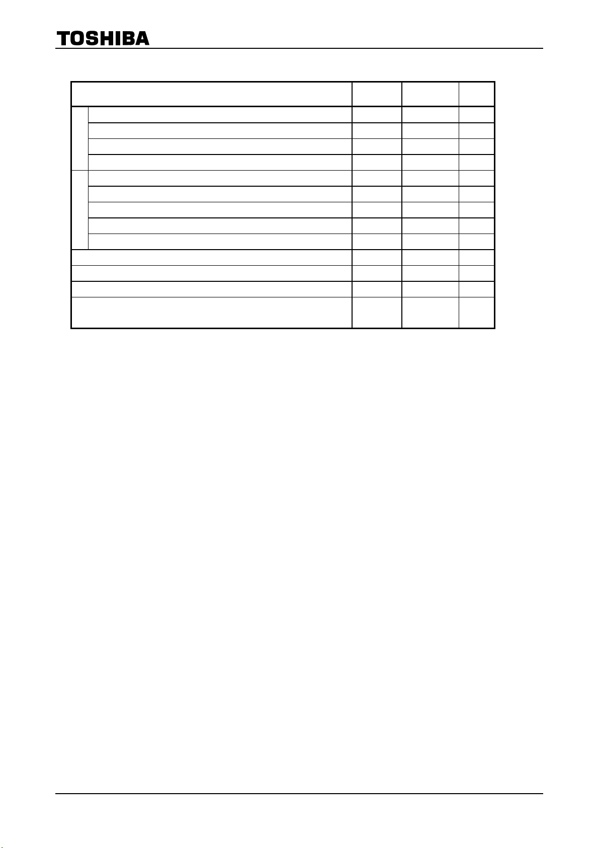
Absolute Maximum Ratings
(Ta = 25°C)
Characteristic Symbol Rating Unit
Forward current (Note 1) I
Pulse forward current (Note 2) I
LDE
Peak transient forward current (Note 3) I
Reverse voltage V
Output current I
Peak output current I
Supply voltage V
Detector
Output voltage V
Output power dissipation (Note 4) P
Operating temperature range T
Storage temperature range T
Lead solder temperature(10 sec.) T
Isolation Voltage
(AC,1 min., R.H.≤ 60°%) (Note 5)
FPT
BV
F
FP
O
OP
CC
opr
stg
sol
R
O
O
S
20 mA
40 mA
1 A
5 V
8 mA
16 mA
−0.5~30 V
−0.5~20 V
100 mW
−55~100
−55~125
260
°C
°C
°C
3750 Vrms
Note: Using continuously under heavy loads (e.g. the application of high temperature/current/voltage and the
significant change in temperature, etc.) may cause this product to decrease in the reliability significantly even
if the operating conditions (i.e. operating temperature/current/voltage, etc.) are within the absolute maximum
ratings.
Please design the appropriate reliability upon reviewing the Toshiba Semiconductor Reliability Handbook
(“Handling Precautions”/“Derating Concept and Methods”) and individual reliability data (i.e. reliability test
report and estimated failure rate, etc).
(Note 1) Derate 0.36mA / °C above 70°C.
(Note 2) 50% duty cycle, Ims pulse width.
Derate 0.72mA / °C above 70°C.
(Note 3) Pulse width≤ 1μs, 300pps.
(Note 4) Derate 1.8mW / °C above 70°C.
2
2007-10-01
TLP114A
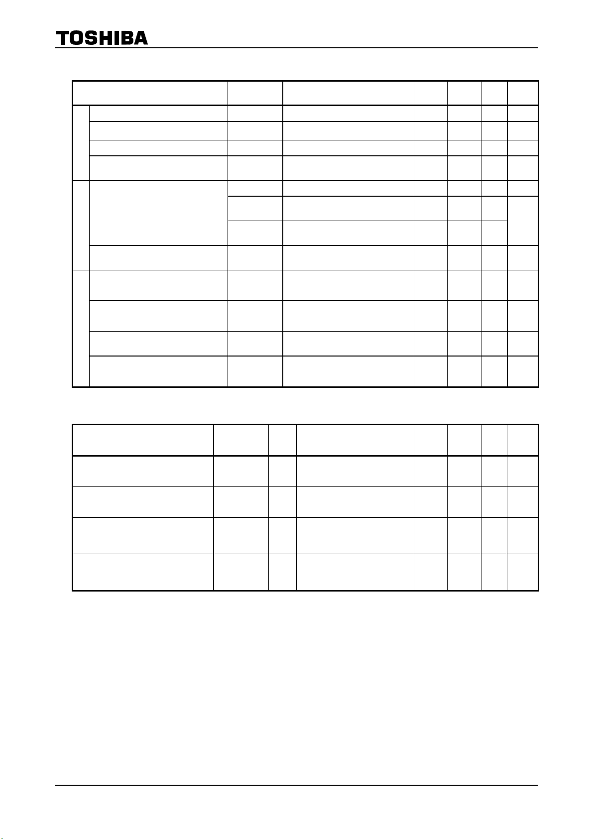
Electrical Characteristics
Characteristic Symbol Test Condition Min. Typ. Max. Unit
Forward voltage V
Forward voltage
temperature coefficient
Reverse current I
LDE
Capacitance between
terminals
High level output
current
Detector
High level supply
current
Current transfer ratio IO / I
Low level output
voltage
Coupled
Isolation resistance RS
Stray capacitance
between input to output
Switching Characteristics
(Ta = 25°C)
IF = 16mA 1.22 1.42 1.72 V
F
/ ΔTa IF = 16mA
ΔV
F
VR = 3V
R
VF = 0, f = 1MHz
C
T
I
OH (1)
I
OH (2)
I
OH
I
CCH
IF = 0mA, VCC = VO = 5.5V
IF = 0mA, VCC = 30V
V
O
IF = 0mA, VCC = 30V
V
O
IF = 0mA, VCC = 30V
= 20V
= 20V, Ta = 70°C
IF = 16mA, VCC = 4.5V
F
V
OL
= 0.4V
V
O
IF = 16mA, VCC = 4.5V
= 2.4 mA
I
O
R.H.≤ 60%, V
(Note 5)
VS= 0, f = 1MHz (Note 5)
C
S
(Ta = 25°C, VCC = 5V)
= 500V
S
―
― ―
―
―
― ―
― ―
―
20
― ―
10
1014
5×10
―
−2
―
mV /°C
10 μA
30
―
pF
3 500 nA
5
μA
50
0.01 1 μA
― ―
%
0.4 V
Ω
―
0.8
―
pF
Characteristic Symbol
Propagation delay time
(H→ L)
Propagation delay time
(L→ H)
Common mode transient
immunity at high output
level
Common mode transient
immunity at low output
level
Test
Cir−
cuit
1
t
pHL
1
t
pLH
2
C
MH
C
ML
I
= 0→ 16mA
F
V
CC
IF = 16→ 0mA
V
CC
I
= 0mA,
F
V
CM
RL = 4.1kΩ
I
= 16mA,
F
2
V
CM
RL = 4.1kΩ
Test Condition Min. Typ. Max. Unit
= 5V, RL = 1.9kΩ
= 5V, RL = 1.9kΩ
= 400V
p−p
= 400V
p−p
― ―
― ―
5000 10000
−5000 −10000
0.8 μs
0.8 μs
―
―
V / μs
V / μs
3
2007-10-01

(Note 5) Device considered a two−terminal device: Pins 1 and 3 shorted together, and pins 4,
5 and 6 shorted together.
(Note 6) Maximum electrostatic discharge voltage for any pins: 100V(C=200pF, R=0)
Test Circuit 1: Switching Time Test Circuit
TLP114A
PULSE INPUT
PW = 100μs
DUTY RATIO = 1/10
MONITOR
I
F
IF
1
3
100Ω
6
5
4
VCC = 5V
RL
V
OUTPUT
MONITOR
O
I
0
VO
F
Test Circuit =2: Common Mode Transient Immunity Test Circuit
= 5V
V
IF
1
3
PULSE GEN
= 50Ω
Z
O
320(V)
CM
=
H
CM
L
μ
s)(rt
,
VCM
320(V)
=
6
5
4
μ
s)(rt
CC
RL
V
OUTPUT
MONITOR
V
CM
O
t
r
VO
(I
= 0mA)
F
V
O
(I
= 16mA)
F
1.5V
t
pHL
5V
1.5V
V
OL
t
pLH
90%
10%
t
f
400V
0V
5V
2V
0.8V
V
OL
4
2007-10-01

TLP114A
ΔV
/ Δta – IF
F
100
I
F
– VF
-4.0
Ta = 70 °C
10
(mA)
F
0
0.1
Forward current I
0.01
1.0
1.2
Forward voltage V
300
VF = 1V
VCC = 5.5V
100
VO = 5.5V
50
30
(nA)
10
OH(1)
5
I
3
High level output currency
1
0.5
20 60 100 120
0
Ambient temperature Ta (°C)
40
1.4
I
0°C
25°C
OH(1)
– Ta
1.6
(V)
F
80
1.8
2.0
Forward voltage temperature
-3.6
-3.2
-2.8
/ Δta (mV / °C )
F
-2.4
-2.0
-1.6
coefficient ΔV
-1.2
0.1
10
VCC = 5V
VO = 0.4V
3
Ta = 25°C
(mA)
1
O
0.5
0.3
0.1
0.05
Output current I
0.03
0.01
0.3 0.5
1
Forward current I
I
O
0.5
0.3 0.1
1
Forward current I
– IF
3 5
(mA)
F
5 3
(mA)
F
10 30
30
10
50
(%)
F
/ I
O
I
Current transfer ratio
100
50
30
10
/ IF – IF
I
O
Ta = 25 °C
100°C
25°C
5
3
- 25°C
VCC = 5V
VO = 0.4V
)
F
I
O /
(I
F
I
O /
Nor,alized I
1.2
1.0
0.8
0.6
0.4
I
O
/ IF – Ta
Normalized to
VCC = 4.5V
VO = 0.4V
Ta = 25°C
IF = 16mA
8mA
1
0.1
0.3
3
1 0.5
Forward current I
(mA)
F
10 5
30
50
0
0 20
40
60
100
80 -20
Ambient temperature Ta (°C)
5
2007-10-01

TLP114A
V
O L
– Ta
VCC = 5V
20
I
O
– VO
VCC = 5V
Ta = 25 °C
0.4
(mA)
O
Output current I
(μs)
pLH
t
pHL,
t
Propagation delay time
16
12
0.5
0.3
8
4
0
0
5
3
1
IF = 16mA
VCC = 5V
Ta = 25 °C
1
2
Output voltage V
t
pHL, tpLH
t
pLH
– RL
t
pHL
25mA
20mA
15mA
10mA
IF = 5mA
(V)
O
0.3
IF = 16mA
(V)
0.2
OL
V
Low level output voltage
4 3
5
0.1
0
- 25
8mA
25 50
IO = 2.4mA
1.1mA
75
100 0
Ambient temperature Ta (°C)
t
pHL, tpLH
3
1
– Ta
IF = 16mA
VCC = 5V
RL = 1.9kΩ
(μs)
pLH
t
pHL,
t
0.5
0.3
t
pLH
Propagation delay time
t
pHL
0.1
1
Load resistance R
10
5
L
30 3
(kΩ)
50
100
0.1
0
40
60 20
Ambient temperature Ta (°C)
80
100
6
2007-10-01

TLP114A
RESTRICTIONS ON PRODUCT USE
• The information contained herein is subject to change without notice.
• TOSHIBA is continually working to improve the quality and reliability of its products. Nevertheless, semiconductor
devices in general can malfunction or fail due to their inherent electrical sensitivity and vulnerability to physical
stress. It is the responsibility of the buyer, when utilizing TOSHIBA products, to comply with the standards of
safety in making a safe design for the entire system, and to avoid situations in which a malfunction or failure of
such TOSHIBA products could cause loss of human life, bodily injury or damage to property.
In developing your designs, please ensure that TOSHIBA products are used within specified operating ranges as
set forth in the most recent TOSHIBA products specifications. Also, please keep in mind the precautions and
conditions set forth in the “Handling Guide for Semiconductor Devices,” or “TOSHIBA Semiconductor Reliability
Handbook” etc.
• The TOSHIBA products listed in this document are intended for usage in general electronics applications
(computer, personal equipment, office equipment, measuring equipment, industrial robotics, domestic appliances,
etc.).These TOSHIBA products are neither intended nor warranted for usage in equipment that requires
extraordinarily high quality and/or reliability or a malfunction or failure of which may cause loss of human life or
bodily injury (“Unintended Usage”). Unintended Usage include atomic energy control instruments, airplane or
spaceship instruments, transportation instruments, traffic signal instruments, combustion control instruments,
medical instruments, all types of safety devices, etc.. Unintended Usage of TOSHIBA products listed in his
document shall be made at the customer’s own risk.
• The products described in this document shall not be used or embedded to any downstream products of which
manufacture, use and/or sale are prohibited under any applicable laws and regulations.
• The information contained herein is presented only as a guide for the applications of our products. No
responsibility is assumed by TOSHIBA for any infringements of patents or other rights of the third parties which
may result from its use. No license is granted by implication or otherwise under any patents or other rights of
TOSHIBA or the third parties.
20070701-EN
• GaAs(Gallium Arsenide) is used in this product. The dust or vapor is harmful to the human body. Do not break,
cut, crush or dissolve chemically.
• Please contact your sales representative for product-by-product details in this document regarding RoHS
compatibility. Please use these products in this document in compliance with all applicable laws and regulations
that regulate the inclusion or use of controlled substances. Toshiba assumes no liability for damage or losses
occurring as a result of noncompliance with applicable laws and regulations.
7
2007-10-01
 Loading...