

Toshiba TLP114A Datasheet
TOSHIBA Photocoupler GaAℓAs Ired & Photo−IC
TLP114A
Digital Logic Isolation.
Line Receiver.
Power Supply Control Feedback Control.
Switching Power Supply.
Transistor Invertor.
The TOSHIBA mini flat coupler TLP114A is a small outline coupler,
suitable for surface mount assembly.
TLP114A consists of a high output power GaAℓAs light emitting didoe,
optically coupled to a high speed detector of one chip
photodiode-transistor.
· Isolation voltage: 3750 Vrms (min.)
· Switching speed: t
(RL = 1.9 kΩ)
· TTL compatible
· UL recognized: UL1577, file no. E67349
p
HL
= 0.8µs, t
= 0.8µs (max.)
LH
p
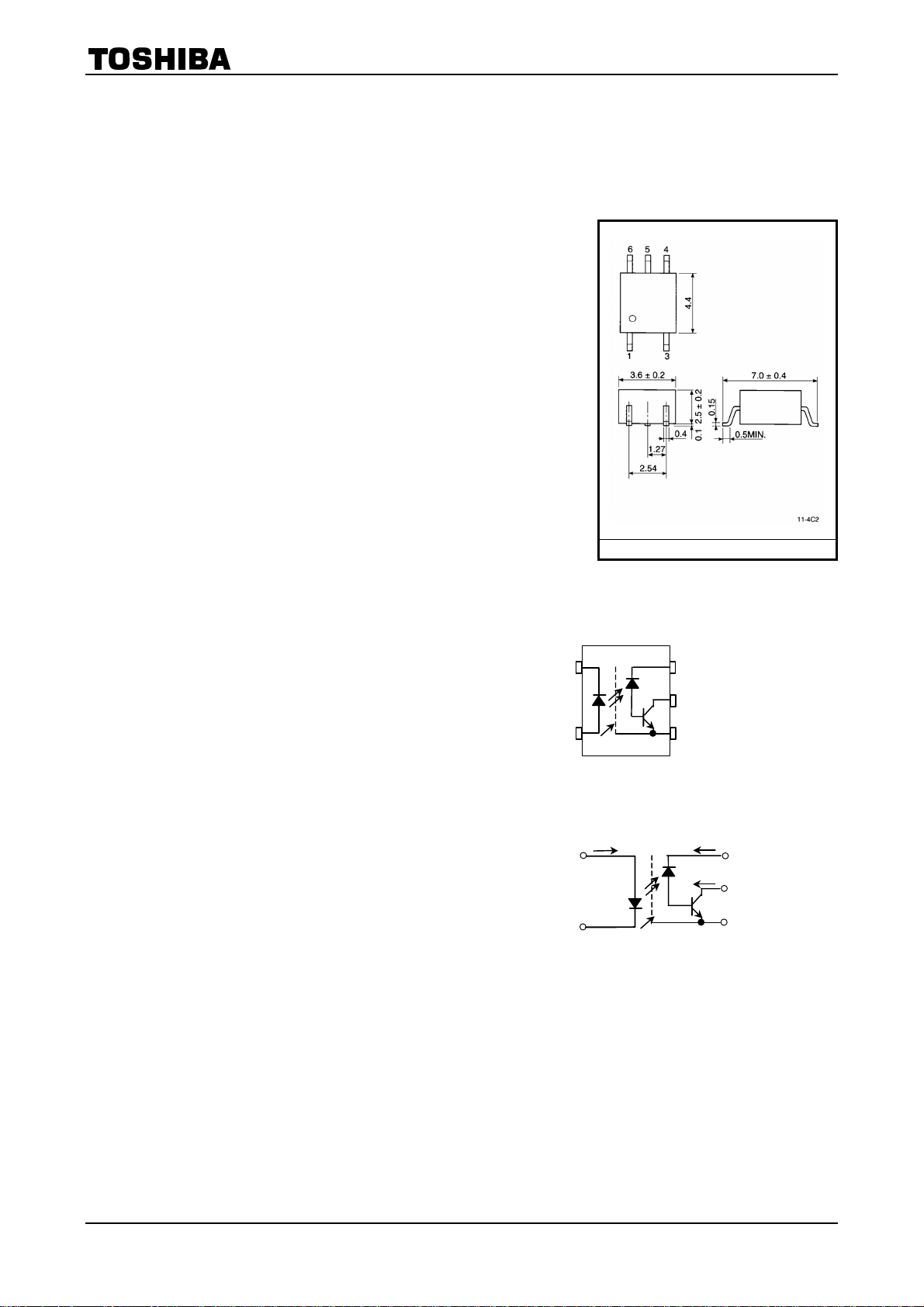
TLP114A
Unit in mm
TOSHIBA 11−4C2
Weight: 0.09g
Pin Configuration (top view)
1 : ANODE
1
3
SHIELD
6
3 : CATHODE
4 : EMITTER (GND)
5
5 : COLLECTOR (OUTPUT).
6 : V
4
CC
Schematic
IF
1
V
F
3
SHIELD
ICC
I
O
VCC
6
V
O
5
GND
4
1
2002-09-25
TLP114A
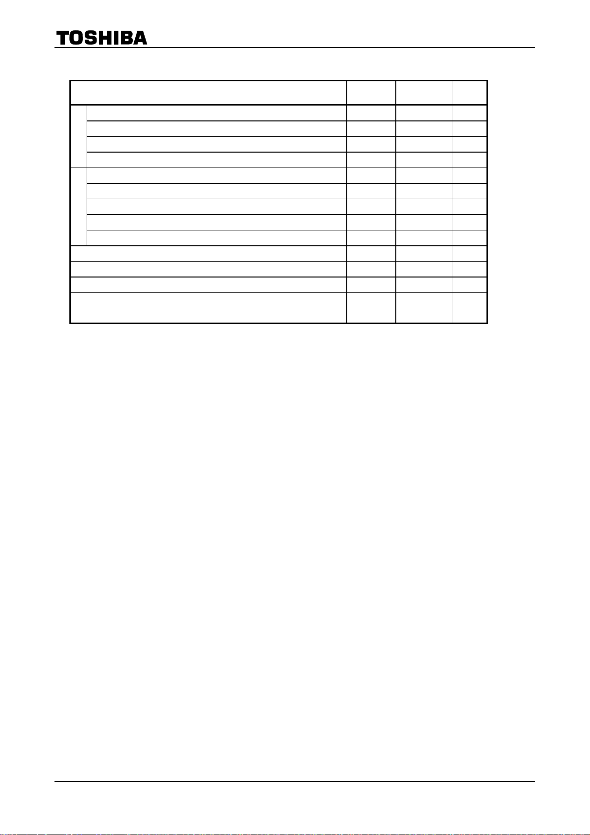
Maximum Ratings
(Ta = 25°C)
Characteristic Symbol Rating Unit
Forward current (Note 1) I
Pulse forward current (Note 2) I
LDE
Peak transient forward current (Note 3) I
Reverse voltage V
Output current I
Peak output current I
Supply voltage V
Detector
Output voltage V
Output power dissipation (Note 4) P
Operating temperature range T
Storage temperature range T
Lead solder temperature(10 sec.) T
Isolation Voltage
(AC,1 min., R.H.≤ 60°%) (Note 5)
(Note 1) Derate 0.36mA / °C above 70°C.
(Note 2) 50% duty cycle, Ims pulse width.
FPT
BV
F
FP
O
OP
CC
opr
stg
sol
R
O
O
S
20 mA
40 mA
1 A
5 V
8 mA
16 mA
-0.5~30 V
-0.5~20 V
100 mW
-55~100
-55~125
260
3750 Vrms
°C
°C
°C
Derate 0.72mA / °C above 70°C.
(Note 3) Pulse width≤ 1µs, 300pps.
(Note 4) Derate 1.8mW / °C above 70°C.
2
2002-9-25
TLP114A
Electrical Characteristics
Characteristic Symbol Test Condition Min. Typ. Max. Unit
Forward voltage V
Forward voltage
temperature coefficient
Reverse current I
LDE
Capacitance between
terminals
High level output
current
Detector
High level supply
current
Current transfer ratio IO / I
Low level output
voltage
Coupled
Isolation resistance RS
Stray capacitance
between input to output
Switching Characteristics
(Ta = 25°C)
IF = 16mA 1.22 1.42 1.72 V
F
∆V
/ ∆Ta IF = 16mA
F
VR = 3V
R
C
VF = 0, f = 1MHz
T
I
OH (1)
I
OH (2)
I
OH
I
CCH
IF = 0mA, VCC = VO = 5.5V
IF = 0mA, VCC = 30V
V
O
IF = 0mA, VCC = 30V
V
O
IF = 0mA, VCC = 30V
= 20V
= 20V, Ta = 70°C
IF = 16mA, VCC = 4.5V
F
V
OL
= 0.4V
V
O
IF = 16mA, VCC = 4.5V
= 2.4 mA
I
O
R.H.≤ 60%, V
(Note 5)
VS= 0, f = 1MHz (Note 5)
C
S
(Ta = 25°C, VCC = 5V)
= 500V
S
―
― ―
―
―
― ―
― ―
―
20
― ―
10
5´10
1014
―
-2
―
mV /°C
10 µA
30
―
pF
3 500 nA
5
µA
50
0.01 1 µA
― ―
%
0.4 V
Ω
―
0.8
―
pF
Characteristic Symbol
Propagation delay time
(H→ L)
Propagation delay time
(L→ H)
Common mode transient
imunity at high output
level
Common mode transient
imunity at low output
level
Test
Cir-
cuit
1
t
pHL
1
t
pLH
C
2
MH
C
ML
I
= 0→ 16mA
F
V
CC
IF = 16→ 0mA
V
CC
= 0mA,
I
F
V
CM
RL = 4.1kΩ
= 16mA,
I
F
2
V
CM
RL = 4.1kΩ
Test Condition Min. Typ. Max. Unit
= 5V, RL = 1.9kΩ
= 5V, RL = 1.9kΩ
= 400V
p-p
= 400V
p-p
― ―
― ―
5000 10000
-5000 -10000
0.8 µs
0.8 µs
―
―
V / µs
V / µs
3
2002-9-25
 Loading...