


查询TLP1031A供应商
TOSHIBA Photointerrupter Infrared LED + Photo IC
TLP1031A
TLP1031A
Domestic electrical appliances such as VTRs and
CD players
Office equipment such as photocopiers, printers
and fax machines
Trackballs
Position detectors
The TLP1031A is a high-withstanding-voltage
photo-interrupter for digital output. The device combines a
high-optical-output GaAs infrared LED with a high-sensitivity,
high-gain Si photo-IC. The photo-IC, which supports a wide
range of systems (3.3 V to 12 V), enables the device to consume
less power than conventional devices. The device also features
a narrow slit width and high resolution.
· Compact package:
Package height: 7.4 mm
Depth: 4.5 mm
· Designed for direct mounting on printed circuit boards
(positioning pins included)
· Gap: 2 mm
· High resolution: Slit width of 0.15 mm
· Digital output (open-collector, high-level output when no light is present)
· Direct connection to logic IC
· Power supply voltage: V
· Switching time: t
· Detector impermeable to visible light
· Package material: Polybutylene-terephthalate (UL94V-0, black)
pLH
Maximum Ratings
= 2.7 V~15 V
CC
= 15 µs (max)
(Ta ==== 25°C)
TOSHIBA ―
Weight: 0.4 g (typ.)
Characteristics Symbol Rating Unit
Forward current I
Forward current derating
LED
Reverse voltage VR 5 V
Supply voltage V
Output voltage VO 15 V
Detector
Low-level output current (Ta = T
Operating temperature T
Storage temperature T
Soldering temperature (5 s) (Note 1) T
Note 1: Soldering is performed 1.5 mm from the bottom of the package.
(Ta > 25°C) -0.33
(Ta > 85°C)
) IOL 16 mA
opr
F
DIF/°C
CC
-30~95 °C
opr
-40~100 °C
stg
260 °C
sol
1
50 mA
mA/°C
-2
15 V
2002-09-20

Recommended Operating Conditions
Characteristics Symbol Min Typ. Max Unit
TLP1031A
LED forward current IF
Supply voltage VCC 2.7 3.3 13.2 V
Output voltage VO ¾ ¾ 13.2 V
Low-level output current IOL ¾ ¾ 16 mA
Operating temperature T
opr
13.4
(Note 2)
-25 ¾ 85 °C
¾ 20 mA
Note 2: The value 13.4 mA takes account of 50% LED optical fluctuation. The initial value of the threshold input
current is 6.7 mA or less.
Electrical and Optical Characteristics
(unless otherwise specified: Ta ==== ----30~95°C, V
Characteristics Symbol Test Conditions Min Typ. Max Unit
Forward voltage VF IF = 10 mA, Ta = 25°C 1.00 1.15 1.30 V
Reverse current IR VR = 5 V, Ta = 25°C ¾ ¾ 10 mA
LED
Peak emission wavelength lP IF = 15 mA, Ta = 25°C ¾ 940 ¾ nm
operating supply voltage VCC ¾ 2.7 ¾ 15 V
Low-level supply current I
High-level supply current I
Detector
Low-level output voltage VOL
High-level output current IOH IF = 0, VO = 15 V ¾ ¾ 6.3 mA
Peak sensitivity wavelength lP Ta = 25°C ¾ 900 ¾ nm
H ® L threshold input current I
Hysteresis I
Propagation delay time (L ® H) t
Propagation delay time (H ® L) t
Rise time tr ¾ 0.8 ¾
Propagation characteristics
Fall time tf
FHL/IFLH
==== 2.7~15 V)
CC
IF = 15 mA, Ta = 25°C ¾ ¾ 1.6
CCL
CCH
FHL
pLH
pHL
= 15 mA ¾ ¾ 2.0
I
F
IF = 0 ¾ ¾ 1.2 mA
IOL = 16 mA, IF = 15 mA,
Ta = 25°C
= 16 mA, IF = 15 mA ¾ ¾ 0.4
I
OL
Ta = 25°C ¾ ¾ 4
¾ ¾ 1.5 ¾
¾ ¾ 15
¾ ¾ 9
= 3.3 V, IF = 15 mA,
V
CC
R
= 10 kW, Ta = 25°C (Note 3)
L
¾ 0.05 0.3
¾ ¾ 6.7
¾ 0.02 ¾
mA
V
mA
ms
Note 3: The switching time measurement circuit and waveform are as follows:
IF
Constant-voltage
circuit
Amp
10 k9
R
L
VCC = 3.3 V
V
OUT
I
V
2
F
OUT
t
pHL
50%
t
pLH
V
OH
90%
1.5 V
10%
t
f
VOL
tr
2002-09-20

TLP1031A
Markings
Monthly lot number
Month of manufacture (January to December denoted by letters A to L respectively)
Year of manufacture (Last digit of year of manufacture)
Precautions
· When removing flux with chemicals after soldering, clean only the soldered part of the leads. Do not immerse
the entire package in the cleaning solvent. Chemical residue on the LED emitter or the photodetector inside the
photo-IC case may adversely affect the optical characteristics of the device and may drastically reduce the
threshold input current.
· The case is made of polybutylene-terephthalate. Oil or chemicals may cause the package to melt or crack. Care
must be taken in relation to the environment in which the device is to be installed.
· Mount the device on a level surface.
· Output fluctuates for 100 ms after power-on while the internal circuit stabilizes.
· To stabilize the power line, insert a bypass capacitor of up to 0.01 mF between V
· The threshold input current increases over time due to current flowing in the infrared LED. The design of
circuits which incorporate the device must take into account the change in threshold input current over time.
The change in threshold input current is equal to the reciprocal of the change in LED infrared optical output.
and GND, close to the device.
CC
1
-
FHL
)t(
ç
=
ç
)0(
è
I
I
FHL
· Choose a high-quality shutter material which is impermeable to light. If the material is of inferior quality, light
from the LED may pass through the shutter, causing the device to malfunction.
æ
ö
)t(OP
÷
÷
)0(OP
ø
3
2002-09-20

Package Dimensions
A
TLP1031A
Product number (TL omitted)
Center of sensor
Country of origin
node
Unit: mm
Slit width
( ): reference value
Weight: 0.4 g (typ.)
Pin Connection
1
2
Constant-voltage
circuit
Amp
1: Anode
2: Cathode
3: V
CC
4: OUT
5: GND
3
4
5
4
2002-09-20

TLP1031A
60
50
(mA)
F
40
30
20
Permissible forward current I
10
0
-20
0 20 40 60 80 100
Ambient temperature Ta (°C)
0.1
Ta = 25°C
VCC = 3.3 V
0.05
(V)
IF = 15 mA
OL
0.03
0.01
0.005
0.003
Low-level output voltage V
0.002
0.3
0.5 1 3 5 10 30
Low-level output current IOL (mA)
t
20
Ta = 25°C
10
VCC = 3.3 V
5
IF = 15 mA
3
(ms)
f
1
, t
r
0.5
0.3
0.1
Rise/Fall time t
0.05
0.03
0.01
0.1
0.3 0.5 1 3 5 10 30 50 100 300 500
Load resistance RL (k9)
– Ta
I
F
VOL – I
, tf – R
r
tr
tf
OL
100
50
30
(mA)
F
10
5
3
Forward current I
1
0.8 0.9 1.0 1.1 1.2
Forward voltage VF (V)
IF – V
F
-25 0 2550Ta = 75°C
(typ.)
1.3 1.4
(typ.)
t
5
Ta = 25°C
(ms)
pHL
, t
pLH
Propagation delay time t
VCC = 3.3 V
4
RL = 10 kW
3
2
1
0
0
10 20 30 40 50 60
Forward current IF (mA)
pLH
, t
pHL
– I
F
t
t
pLH
pHL
(typ.)
L
(typ.)
t
7
Ta = 25°C
6
(ms)
pHL
, t
pLH
Propagation delay time t
VCC = 3.3 V
IF = 15 mA
5
4
3
2
1
0
0.1 0.3
0.5 1 3 5 10 30 50 100
Load resistance RL (k9)
pLH
, t
pHL
– R
L
t
t
pLH
pHL
(typ.)
5
2002-09-20
A
A
+
Detection position characteristic (typ.)
1.2
1.0
0.8
0.6
0.4
Relative output voltage
0.2
0
-0.4
-0.2 0 0.2 0.4 0.6 0.8
Ta = 25°C
VCC = 3.3 V
RL = 10 kW
IF = 20 mA
Shutter
Detection position
d = 0 ± 0.11 mm
Distance d (mm)
0 +-
d
Relative Positioning of Shutter and Device
TLP1031A
Detection position characteristic (typ.)
1.2
1.0
0.8
0.6
0.4
Relative output voltage
0.2
0
4.2
4.4 4.6 4.8 5.0 5.2
Distance d (mm)
Ta = 25°C
VCC = 3.3 V
RL = 10 kW
IF = 20 mA
Shutter
Detection position
1.1
d = 5.5 mm
-1.5
d
5.4
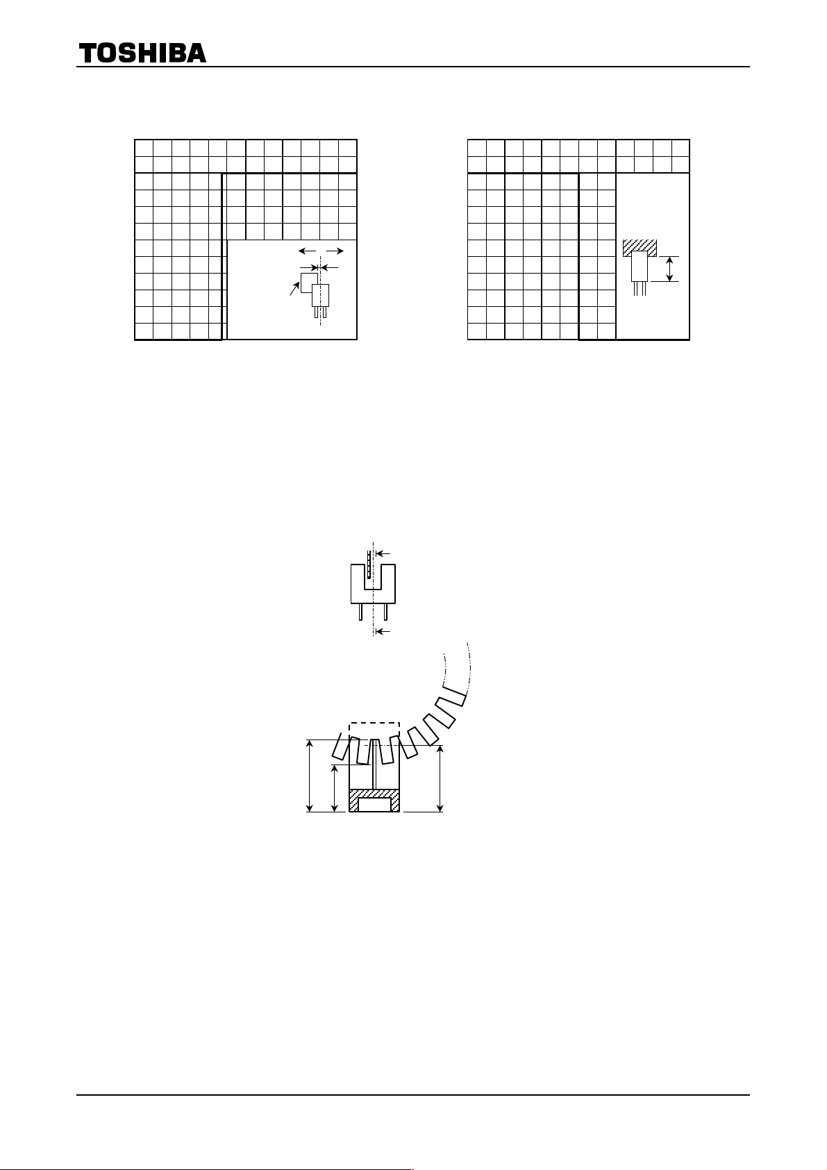
For normal operation, position the shutter and the device as shown in the figure below. By considering the
device’s detection direction characteristic and switching time, determine the shutter slit width and pitch.
’
Unit: mm
Center of sensor
6.6 min
4 max
5.5
Cross section between A and A’
6
2002-09-20

TLP1031A
RESTRICTIONS ON PRODUCT USE
· TOSHIBA is continually working to improve the quality and reliability of its products. Nevertheless, semiconductor
devices in general can malfunction or fail due to their inherent electrical sensitivity and vulnerability to physical
stress. It is the responsibility of the buyer, when utilizing TOSHIBA products, to comply with the standards of
safety in making a safe design for the entire system, and to avoid situations in which a malfunction or failure of
such TOSHIBA products could cause loss of human life, bodily injury or damage to property.
In developing your designs, please ensure that TOSHIBA products are used within specified operating ranges as
set forth in the most recent TOSHIBA products specifications. Also, please keep in mind the precautions and
conditions set forth in the “Handling Guide for Semiconductor Devices,” or “TOSHIBA Semiconductor Reliability
Handbook” etc..
· The TOSHIBA products listed in this document are intended for usage in general electronics applications
(computer, personal equipment, office equipment, measuring equipment, industrial robotics, domestic appliances,
etc.). These TOSHIBA products are neither intended nor warranted for usage in equipment that requires
extraordinarily high quality and/or reliability or a malfunction or failure of which may cause loss of human life or
bodily injury (“Unintended Usage”). Unintended Usage include atomic energy control instruments, airplane or
spaceship instruments, transportation instruments, traffic signal instruments, combustion control instruments,
medical instruments, all types of safety devices, etc.. Unintended Usage of TOSHIBA products listed in this
document shall be made at the customer’s own risk.
· Gallium (GaAs) Arsenide is a substance used in the products described in this document. GaAs dust or vapor is
harmful to the human body. Do not break, cut, crushu or dissolve chemically.
· The products described in this document are subject to the foreign exchange and foreign trade laws.
· The information contained herein is presented only as a guide for the applications of our products. No
responsibility is assumed by TOSHIBA CORPORATION for any infringements of intellectual property or other
rights of the third parties which may result from its use. No license is granted by implication or otherwise under
any intellectual property or other rights of TOSHIBA CORPORATION or others.
020704EBC
· The information contained herein is subject to change without notice.
7
2002-09-20
 Loading...