

查询TLFGE53T供应商
TL(RE,RME,SE,OE,YE,PYE,GE,FGE,PGE)53T
TOSHIBA InGaAℓP LED
TLRE53T,TLRME53T,TLSE53T,TLOE53T,TLYE53T,
TLPYE53T,TLGE53T,TLFGE53T,TLPGE53T
Panel Circuit Indicators
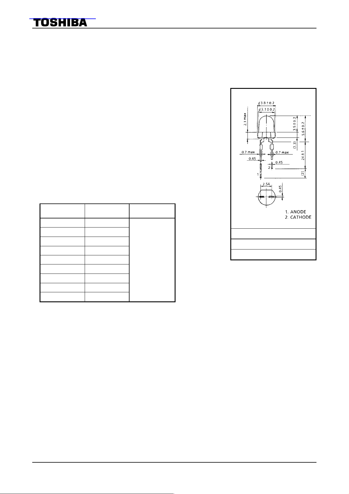
· φ3 mm package
· InGaAℓP technology
· All plastic mold
· Transparent lens
· Line-up: 6 colors (red, orange, yellow, pure yellow, green and pure
green)
· High intensity light emission
· Excellent low current light output
· Applications: message boards, security devices and dashboard
displays
Line-up
Unit: mm
Product Name Color Material
TLRE53T Red
TLRME53T Red
TLSE53T Red
TLOE53T Orange
TLYE53T Yellow
TLPYE53T Pure Yellow
TLGE53T Green
TLFGE53T Green
TLPGE53T Pure Green
PInGaAl
JEDEC ―
JEITA ―
TOSHIBA 4-4E1A
Weight: 0.14 g
1
2002-01-17
TL(RE,RME,SE,OE,YE,PYE,GE,FGE,PGE)53T
Maximum Ratings
Product Name
TLRE53T 50 4 120
TLRME53T 50 4 120
TLSE53T 50 4 120
TLOE53T 50 4 120
TLYE53T 50 4 120
TLPYE53T 50 4 120
TLGE53T 50 4 120
TLFGE53T 50 4 120
TLPGE53T 50 4 120
(Ta ==== 25°C)
Forward Current
I
(mA)
F
Reverse Voltage
VR (V)
Power Dissipation
PD (mW)
Operating
Temperature
(°C)
T
opr
-40~100 -40~120
Storage
Temperature
T
stg
Electrical and Optical Characteristics
Product Name
TLRE53T 630 (644) 20 20 153 400 20 1.9 2.4 20 50 4
TLRME53T 626 (636) 23 20 272 600 20 1.9 2.4 20 50 4
TLSE53T 613 (623) 20 20 272 800 20 1.9 2.4 20 50 4
TLOE53T 605 (612) 20 20 272 1000 20 2.0 2.4 20 50 4
TLYE53T 587 (590) 17 20 272 800 20 2.0 2.4 20 50 4
TLPYE53T 580 (583) 14 20 153 450 20 2.0 2.4 20 50 4
TLGE53T 571 (574) 17 20 153 400 20 2.0 2.4 20 50 4
TLFGE53T 565 (568) 15 20 85 200 20 2.0 2.4 20 50 4
TLPGE53T 558 (562) 14 20 47.6 130 20 2.1 2.4 20 50 4
Unit nm mA mcd mA V mA mA V
Typ. Emission Wavelength
lP Dl IF
l
d
(Ta ==== 25°C)
Luminous Intensity
Min Typ. I
I
V
Typ. Max IF Max VR
F
Forward Voltage
VF
Reverse Current
Precautions
(°C)
IR
Please be careful of the following:
· Soldering temperature: 260°C max, soldering time: 3 s max
(soldering portion of lead: up to 2 mm from the body of the device)
· If the lead is formed, the lead should be formed up to 5 mm from the body of the device without forming stress to
the resin. Soldering should be performed after lead forming.
· This visible LED lamp also emits some IR light.
If a photodetector is located near the LED lamp, please ensure that it will not be affected by this IR light.
2
2002-01-17
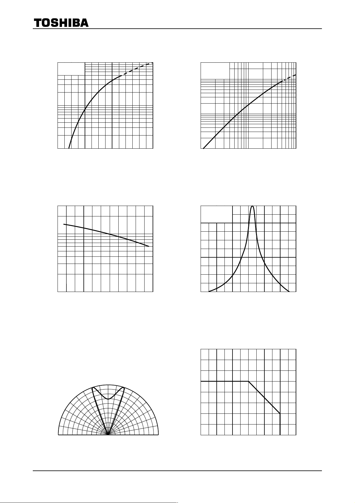
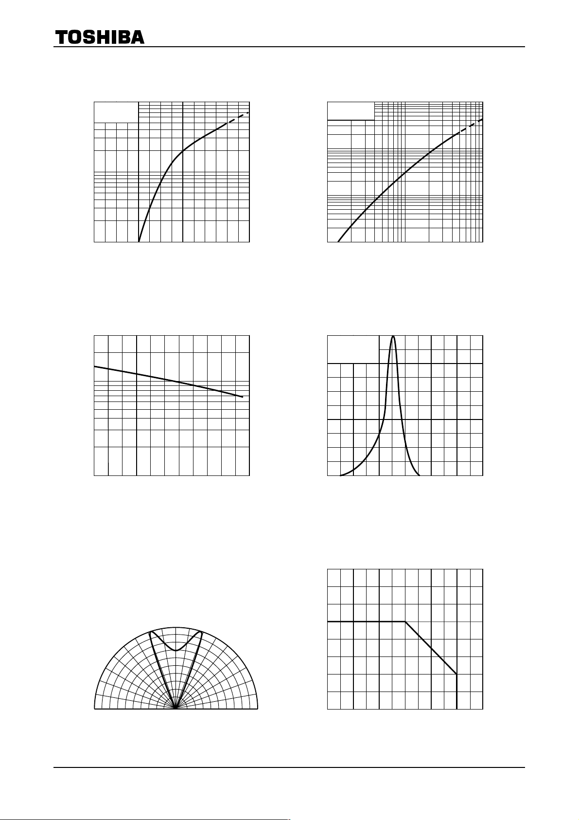
TLRE53T
TL(RE,RME,SE,OE,YE,PYE,GE,FGE,PGE)53T
100
(mA)
F
Forward current I
Ta = 25°C
50
30
10
5
3
– VF
I
F
1
1.6
1.7 1.8 1.9 2.0 2.1 2.2 2.3
Forward voltage VF (V)
I
– IF
3000
Ta = 25°C
1000
(mcd)
V
100
V
Luminous intensity I
10
101
100
Forward current IF (mA)
3
V
I
V
– Tc
1
Relative luminous intensity I
0.5
0.3
0.1
-20 80
0
20
40
Case temperature Tc (°C)
60
Relative luminous intensity – Wavelength
1.0
IF = 20 mA
Ta = 25°C
0.8
0.6
0.4
0.2
Relative luminous intensity
0
700
680 660 640 620600580
Wavelength l (nm)
Radiation pattern
Ta = 25°C
I
– Ta
80
F
50°
60°
70°
80°
90°
40°
30°
20°
10°
0°
10°
20°
30°
40°
50°
60°
70°
80°
90°
1.00.80.6 0.4 0.2 0
(mA)
F
60
40
20
Allowable forward current I
0
0
40 60 80
100
12020
Ambient temperature Ta (°C)
3
2002-01-17
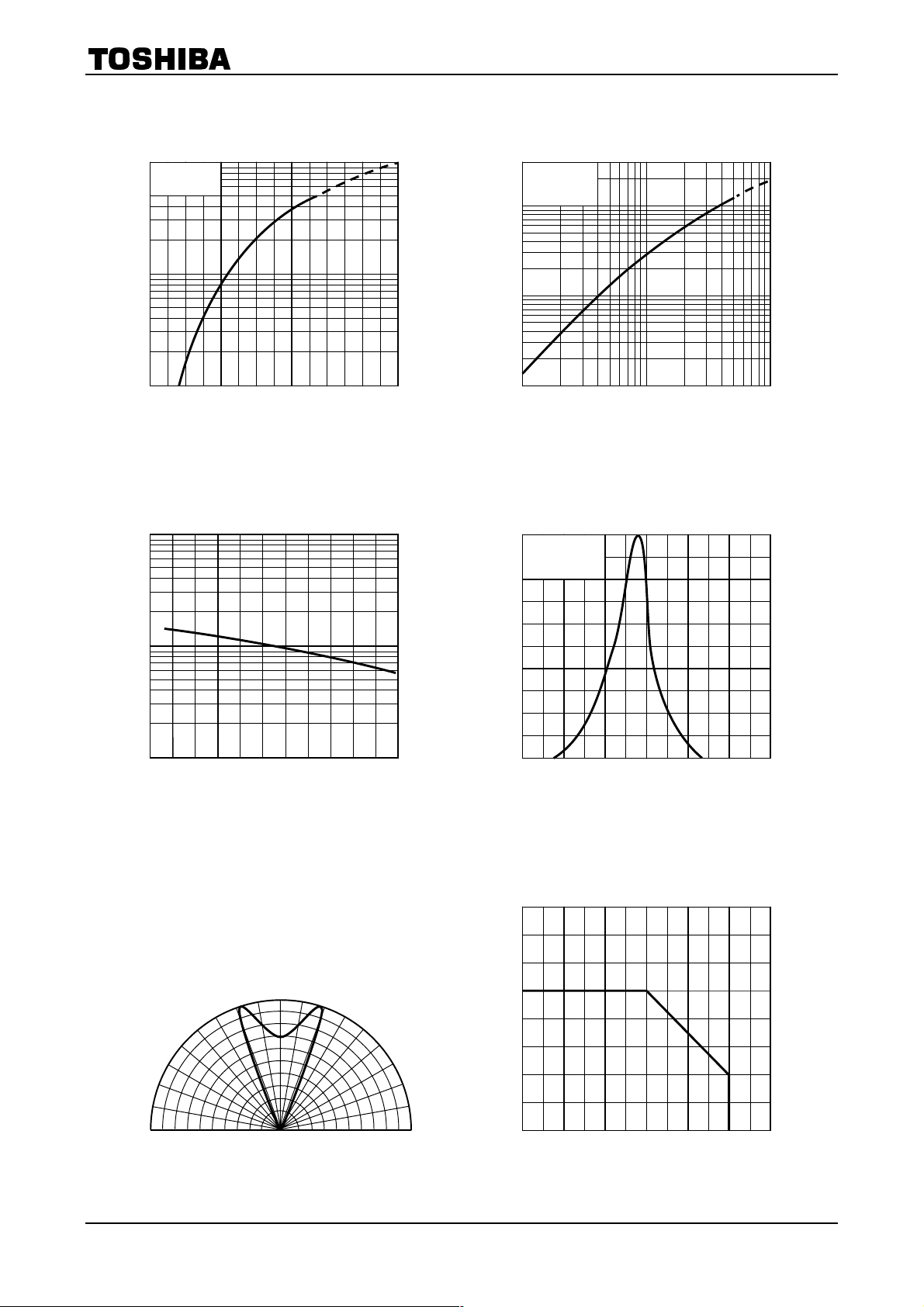
TLRME53T
TL(RE,RME,SE,OE,YE,PYE,GE,FGE,PGE)53T
100
(mA)
F
Forward current I
Ta = 25°C
50
30
10
5
3
– VF
I
F
1
1.6
1.7 1.8 1.9 2.0 2.1 2.2 2.3
Forward voltage VF (V)
I
– IF
3000
Ta = 25°C
1000
(mcd)
V
100
V
Luminous intensity I
10
101
100
Forward current IF (mA)
10
V
5
3
I
V
– Tc
1
Relative luminous intensity I
0.5
0.3
0.1
-20 80
0
20
40
Case temperature Tc (°C)
60
Relative luminous intensity – Wavelength
1.0
IF = 20 mA
Ta = 25°C
0.8
0.6
0.4
0.2
Relative luminous intensity
0
700
680 660 640 620600580
Wavelength l (nm)
Radiation pattern
Ta = 25°C
I
– Ta
80
F
50°
60°
70°
80°
90°
40°
30°
20°
10°
0°
10°
20°
30°
40°
50°
60°
70°
80°
90°
1.00.80.6 0.4 0.2 0
(mA)
F
60
40
20
Allowable forward current I
0
0
40 60 80
100
12020
Ambient temperature Ta (°C)
4
2002-01-17

TLSE53T
TL(RE,RME,SE,OE,YE,PYE,GE,FGE,PGE)53T
100
(mA)
F
Forward current I
Ta = 25°C
50
30
10
5
3
– VF
I
F
1
1.6
1.7 1.8 1.9 2.0 2.1 2.2 2.3
Forward voltage VF (V)
(mcd)
V
Luminous intensity I
10000
1000
100
10
I
– IF
V
Ta = 25°C
101
Forward current IF (mA)
100
3
V
I
V
– Tc
1
Relative luminous intensity I
0.5
0.3
0.1
-20 80
0
20
40
Case temperature Tc (°C)
60
Relative luminous intensity – Wavelength
1.0
IF = 20 mA
Ta = 25°C
0.8
0.6
0.4
0.2
Relative luminous intensity
0
680
660 640 620 600580560
Wavelength l (nm)
Radiation pattern
Ta = 25°C
I
– Ta
80
F
50°
60°
70°
80°
90°
40°
30°
20°
10°
0°
10°
20°
30°
40°
50°
60°
70°
80°
90°
1.00.80.6 0.4 0.2 0
(mA)
F
60
40
20
Allowable forward current I
0
0
40 60 80
100
12020
Ambient temperature Ta (°C)
5
2002-01-17

TLOE53T
TL(RE,RME,SE,OE,YE,PYE,GE,FGE,PGE)53T
100
(mA)
F
Forward current I
Ta = 25°C
50
30
10
5
3
– VF
I
F
1
1.6
1.7 1.8 1.9 2.0 2.1 2.2 2.3
Forward voltage VF (V)
(mcd)
V
Luminous intensity I
10000
1000
100
10
I
– IF
V
Ta = 25°C
101
Forward current IF (mA)
100
3
V
I
V
– Tc
1
Relative luminous intensity I
0.5
0.3
0.1
-20 80
0
20
40
Case temperature Tc (°C)
60
Relative luminous intensity – Wavelength
1.0
IF = 20 mA
Ta = 25°C
0.8
0.6
0.4
0.2
Relative luminous intensity
0
660
640 620 600 580560540
Wavelength l (nm)
Radiation pattern
Ta = 25°C
I
– Ta
80
F
50°
60°
70°
80°
90°
40°
30°
20°
10°
0°
10°
20°
30°
40°
50°
60°
70°
80°
90°
1.00.80.6 0.4 0.2 0
(mA)
F
60
40
20
Allowable forward current I
0
0
40 60 80
100
12020
Ambient temperature Ta (°C)
6
2002-01-17
TLYE53T
TL(RE,RME,SE,OE,YE,PYE,GE,FGE,PGE)53T
100
(mA)
F
Forward current I
Ta = 25°C
50
30
10
5
3
– VF
I
F
1
1.6
1.7 1.8 1.9 2.0 2.1 2.2 2.3
Forward voltage VF (V)
(mcd)
V
Luminous intensity I
10000
1000
100
10
I
– IF
V
Ta = 25°C
101
Forward current IF (mA)
100
3
V
I
V
– Tc
1
Relative luminous intensity I
0.5
0.3
0.1
-20 80
0
20
40
Case temperature Tc (°C)
60
Relative luminous intensity – Wavelength
1.0
IF = 20 mA
Ta = 25°C
0.8
0.6
0.4
0.2
Relative luminous intensity
0
660
640 620 600 580560540
Wavelength l (nm)
Radiation pattern
Ta = 25°C
I
– Ta
80
F
50°
60°
70°
80°
90°
40°
30°
20°
10°
0°
10°
20°
30°
40°
50°
60°
70°
80°
90°
1.00.80.6 0.4 0.2 0
(mA)
F
60
40
20
Allowable forward current I
0
0
40 60 80
100
12020
Ambient temperature Ta (°C)
7
2002-01-17
TLPYE53T
TL(RE,RME,SE,OE,YE,PYE,GE,FGE,PGE)53T
100
(mA)
F
Forward current I
Ta = 25°C
50
30
10
5
3
– VF
I
F
1
1.7 2.1
1.8 1.9 2.2
2.0 1.6
Forward voltage VF (V)
2.3
I
– IF
3000
Ta = 25°C
1000
(mcd)
V
100
Luminous intensity I
10
5
V
101
100
Forward current IF (mA)
10
V
5
3
I
V
– Tc
Relative luminous intensity – Wavelength
1.0
0.8
IF = 20 mA
Ta = 25°C
1
0.5
0.3
Relative luminous intensity I
0.1
Case temperature Tc (°C)
20 -20
0 40 60
80
0.6
0.4
0.2
Relative luminous intensity
0
580540
560 600 620 640
660
Wavelength l (nm)
Radiation pattern
Ta = 25°C
I
– Ta
80
F
(mA)
F
60
60°
70°
80°
90°
30°
40°
50°
20°
10°
10°
20°
30°
40°
50°
60°
70°
1.00.80.6 0.4 0.2 0
80°
90°
40
20
Allowable forward current I
0
0
40 60 80
100
12020
Ambient temperature Ta (°C)
0°
8
2002-01-17

TLGE53T
TL(RE,RME,SE,OE,YE,PYE,GE,FGE,PGE)53T
100
(mA)
F
Forward current I
Ta = 25°C
50
30
10
5
3
– VF
I
F
1
1.6
1.7 1.8 1.9 2.0 2.1 2.2 2.3
Forward voltage VF (V)
I
– IF
5000
Ta = 25°C
1000
(mcd)
V
100
V
Luminous intensity I
10
101
100
Forward current IF (mA)
10
V
5
3
I
V
– Tc
Relative luminous intensity I
1
0.5
0.3
0.1
-20 80
0
20
40
Case temperature Tc (°C)
60
Relative luminous intensity – Wavelength
1.0
IF = 20 mA
Ta = 25°C
0.8
0.6
0.4
0.2
Relative luminous intensity
0
640
620 600 580 560540520
Wavelength l (nm)
Radiation pattern
Ta = 25°C
I
– Ta
80
F
50°
60°
70°
80°
90°
40°
30°
20°
10°
0°
10°
20°
30°
40°
50°
60°
70°
80°
90°
1.00.80.6 0.4 0.2 0
(mA)
F
60
40
20
Allowable forward current I
0
0
40 60 80
100
12020
Ambient temperature Ta (°C)
9
2002-01-17

TLFGE53T
TL(RE,RME,SE,OE,YE,PYE,GE,FGE,PGE)53T
100
Ta = 25°C
50
30
(mA)
F
10
5
3
– VF
I
F
Forward current I
1
1.7 2.1
1.8 1.9 2.2
Forward voltage VF (V)
2.0 1.6
2.3
I
– IF
1000
Ta = 25°C
(mcd)
V
100
10
V
Luminous intensity I
3
101
100
Forward current IF (mA)
10
V
5
3
I
V
– Tc
Relative luminous intensity – Wavelength
1.0
0.8
IF = 20 mA
Ta = 25°C
1
0.5
0.3
Relative luminous intensity I
0.1
Case temperature Tc (°C)
20 -20
0 40 60
80
0.6
0.4
0.2
Relative luminous intensity
0
560520
540 580 600 620
640
Wavelength l (nm)
Radiation pattern
Ta = 25°C
I
– Ta
80
F
50°
60°
70°
80°
90°
40°
30°
20°
10°
0°
10°
20°
30°
40°
50°
60°
70°
80°
90°
1.00.80.6 0.4 0.2 0
(mA)
F
60
40
20
Allowable forward current I
0
0
40 60 80
100
12020
Ambient temperature Ta (°C)
10
2002-01-17

TLPGE53T
TL(RE,RME,SE,OE,YE,PYE,GE,FGE,PGE)53T
100
(mA)
F
Forward current I
Ta = 25°C
50
30
10
5
3
– VF
I
F
1
1.6
1.7 1.8 1.9 2.0 2.1 2.2 2.3
Forward voltage VF (V)
I
– IF
1000
Ta = 25°C
(mcd)
100
V
10
V
Luminous intensity I
1
101
100
Forward current IF (mA)
10
V
5
3
I
V
– Tc
1
Relative luminous intensity I
0.5
0.3
0.1
-20 80
0
20
40
Case temperature Tc (°C)
60
Relative luminous intensity – Wavelength
1.0
0.8
0.6
0.4
0.2
Relative luminous intensity
0
IF = 20 mA
Ta = 25°C
640
620 600 580 560540520
Wavelength l (nm)
Radiation pattern
Ta = 25°C
I
– Ta
80
F
50°
60°
70°
80°
90°
40°
30°
20°
10°
0°
10°
20°
30°
40°
50°
60°
70°
80°
90°
1.00.80.6 0.4 0.2 0
(mA)
F
60
40
20
Allowable forward current I
0
0
40 60 80
100
12020
Ambient temperature Ta (°C)
11
2002-01-17

TL(RE,RME,SE,OE,YE,PYE,GE,FGE,PGE)53T
RESTRICTIONS ON PRODUCT USE
· TOSHIBA is continually working to improve the quality and reliability of its products. Nevertheless, semiconductor
devices in general can malfunction or fail due to their inherent electrical sensitivity and vulnerability to physical
stress. It is the responsibility of the buyer, when utilizing TOSHIBA products, to comply with the standards of
safety in making a safe design for the entire system, and to avoid situations in which a malfunction or failure of
such TOSHIBA products could cause loss of human life, bodily injury or damage to property.
In developing your designs, please ensure that TOSHIBA products are used within specified operating ranges as
set forth in the most recent TOSHIBA products specifications. Also, please keep in mind the precautions and
conditions set forth in the “Handling Guide for Semiconductor Devices,” or “TOSHIBA Semiconductor Reliability
Handbook” etc..
· The TOSHIBA products listed in this document are intended for usage in general electronics applications
(computer, personal equipment, office equipment, measuring equipment, industrial robotics, domestic appliances,
etc.). These TOSHIBA products are neither intended nor warranted for usage in equipment that requires
extraordinarily high quality and/or reliability or a malfunction or failure of which may cause loss of human life or
bodily injury (“Unintended Usage”). Unintended Usage include atomic energy control instruments, airplane or
spaceship instruments, transportation instruments, traffic signal instruments, combustion control instruments,
medical instruments, all types of safety devices, etc.. Unintended Usage of TOSHIBA products listed in this
document shall be made at the customer’s own risk.
· Gallium arsenide (GaAs) is a substance used in the products described in this document. GaAs dust and fumes
are toxic. Do not break, cut or pulverize the product, or use chemicals to dissolve them. When disposing of the
products, follow the appropriate regulations. Do not dispose of the products with other industrial waste or with
domestic garbage.
· The information contained herein is presented only as a guide for the applications of our products. No
responsibility is assumed by TOSHIBA CORPORATION for any infringements of intellectual property or other
rights of the third parties which may result from its use. No license is granted by implication or otherwise under
any intellectual property or other rights of TOSHIBA CORPORATION or others.
000707EAC
· The information contained herein is subject to change without notice.
12
2002-01-17
 Loading...