

Page 1

TOSHIBA Original CMOS 32-Bit Microcontroller
TLCS-900/H1 Series
TMP92CM22FG
Semiconductor Company
Page 2

Preface
Thank you very much for making use of Toshiba microcomputer LSIs.
Before use this LSI, refer the section, “Points of Note and Restrictions”.
Page 3

CMOS 32-Bit Microcontrollers
TMP92CM22FG
1. Outline and Device Characteristics
TMP92CM22 is high-speed advanced 32-bit microcontroller developed for controlling equipment,
which processes mass data.
TMP92CM22FG is a microcontroller, which has a high-performance CPU (900/H1 CPU) and
various built-in I/Os. TMP92CM22F is housed in a 100-pin flat package.
Device characteristics are as follows:
(1) CPU: 32-bit CPU (900/H1 CPU)
• Compatible with TLCS-900, 900/L, 900/L1, 900/H, and 900/H2’s instruction code
• 16 Mbytes of linear address space
• General-purpose register and register banks
TMP92CM22
• Micro DMA: 8 channels (250 ns/4 bytes at f
(2) Minimum instruction execution time: 50 ns (at f
= 20 MHz, best case)
SYS
= 20 MHz)
SYS
(3) Internal memory
• Internal RAM: 32 Kbytes (32-bit 1-clock access, programmable)
• Internal ROM: None
RESTRICTIONS ON PRODUCT USE
• The information contained herein is subject to change without notice. 021023_D
• TOSHIBA is continually working to improve the quality and reliability of its products. Nevertheless, semiconductor
devices in general can malfunction or fail due to their inherent electrical sensitivity an d vulnerability to physical
stress. It is the responsibility of the buyer, when utilizing TOSHIBA products, to comply with the standards of safety
in making a safe design for the entire system, and to avoid situations in which a malfunction or failur e of such
TOSHIBA products could cause loss of human life, bodily injury or damage to property.
In developing your designs, please ensure that TOSHIBA products are used within specified operating ranges as
set forth in the most recent TOSHIBA products specifications. Also, please keep in mind the precautions and
conditions set forth in the “Handling Guide for Semiconductor Devices,” or “TOSHIBA Semiconductor Reliability
Handbook” etc.
• The TOSHIBA products listed in this document are intended for usage in general electronics applications (computer,
personal equipment, office equipment, measuring equipment, industrial robotics, domestic appliances, etc.). These
TOSHIBA products are neither intended nor warranted for usage in equipment that requires extraordinarily high
quality and/or reliability or a malfunction or failure of which may cause loss of human life or bodily injury
(“Unintended Usage”). Unintended Usage include atomic energy control instruments, airplane or spaceship
instruments, transportation instruments, traffic signal instruments, combustion control instruments, medical
instruments, all types of safety devices, etc. Unintended Usage of TOSHIBA products listed in this document shall
be made at the customer’s own risk.
021023_A
021023_B
070208EBP
• The products described in this document shall not be used or embedded to any downstream products of which
manufacture, use and/or sale are prohibited under any applicable laws and regulations. 060106_Q
• The information contained herein is presented only as a guide for the applications of our products. No responsibility
is assumed by TOSHIBA for any infringements of patents or other rights of the third parties which may result from its
use. No license is granted by implication or otherwise under any patents or other rights of TOSHIBA or the third
parties.
021023_C
• The products described in this document are subject to foreign exchange and foreign trade control laws.
• For a discussion of how the reliability of microcontrollers can be predicted, please refer to Section 1.3 of the chapter
entitled Quality and Reliability Assurance/Handling Precautions. 030619_S
92CM22-1
060925_E
2007-02-16
Page 4

TMP92CM22
(4) External memory expansion
• Expandable up to 16 Mbytes (Shared program/data area)
• Can simultaneously support 8-/16-bit width external data bus
・・・Dynamic data bus sizing
• Separate bus system
(5) Memory controller
• Chip select output: 4 channels
(6) 8-bit timers: 4 channels
(7) 16-bit timers: 2 channels
(8) General-purpose serial interface: 2 channels
• UART/synchronous mode
• IrDA
(9) Serial bus interface: 1 channel
2
C bus mode
• I
• Clock synchronous mode
(10) 10-bit AD converter: 8 channels
(11) Watchdog timer
(12) Interrupts: 41 interrupts
• 9 CPU interrupts: Software interrupt instruction and illegal instruction
• 25 internal interrupts: Seven selectable priority levels
• 7 external interrupts: Seven selectable priority levels (INT0 to INT5 and
NMI )
(INT0 to INT3 selectable edge or level interrupt)
(13) Input/output ports: 50 pins (exclude Data bus 8-bit, Address bus 24-bit and
RD pin)
(14) Standby function
• Three HALT modes: IDLE2 (Programmable), IDLE1, STOP
(15) Dual-clock controller
• PLL: fc = f
× 4 (fc = 40 MHz at f
OSCH
OSCH
= 10 MHz)
• Clock gear function: Select a high-frequency clock fc to fc/16
(16) Operating voltage
• DVCC = 3.0 V to 3.6 V (fc max = 40 MHz)
(17) Package
• 100-pin QFP: P-LQFP100-1414-0.50F
92CM22-2
2007-02-16
Page 5
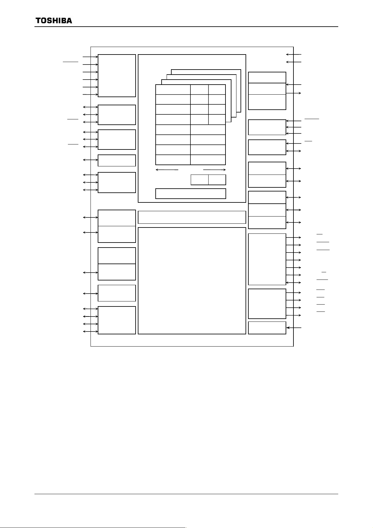
Y
(
PG0 to PG7
(AN0 to AN7)
ADTRG )
PG3 (
AVCC
AVSS
VREFH
VREFL
PF0 (TXD0)
PF1 (RXD0)
PF2 (SCLK0/ CTS0 )
PF3 (TXD1)
PF4 (RXD1)
PF5 (SCLK1/ CTS1 )
PF6 to PF7
P90
SCK)
P91 (SO/SDA)
P92 (SI/SCL)
PC0 (TA0IN)
PC1 (TA1OUT/INT1)
PC5 (TA3OUT/INT2)
PC6 (TB00UT0/INT3)
PD0 (TB1IN0/INT4)
PD1 (TB1IN1/INT5)
PD2 (TB1OUT0)
PD3 (TB1OUT1)
10-bit 8-ch
AD
converter
Serial I/O
SIO0
Serial I/O
SIO1
Port F
Serial
bus I/F
SBI0
8-bit timer
(Timer A0)
8-bit timer
(Timer A1)
8-bit timer
(Timer A2)
8-bit timer
(Timer A3)
16-bit timer
(Timer B0)
16-bit timer
(Timer B1)
XWA
XBC
XDE
XHL
XIX
XI
XIZ
XSP
TMP92CM22
DVCC [3]
900/H1 CPU
PLL
AW
CB
ED
LH
IX
32 bits
SR
P C
Watchdog timer
32-Kbyte RAM
IY
IZ
SP
F
H-OSC
Clock gear
Mode
controller
Interrupt
controller
Data bus
Port 1
Port 4
Port 5
Port 6
Port 7
Port 8
Port A
DVSS [4]
X1
X2
RESET
AM0
AM1
NMI
PC3(INT0)
D0 to D7
P10 to P17
(D8 to D15)
P40 to P47
(A0 to A7)
P50 to P57
(A8 to A15)
P60 to P67
(A16 to A23)
P70 (
RD )
WRLL )
P71 (
P72 (
WRLU )
P73
P74 (CLKOUT)
P75 (R/ W )
P76 ( WAIT )
P80 ( CS0 )
P81 ( CS1 )
CS2 )
P82 (
P83 ( CS3 )
PA0 to PA2
PA7
Figure 1.1 TMP92CM22 Block Diagram
92CM22-3
2007-02-16
Page 6
A
A
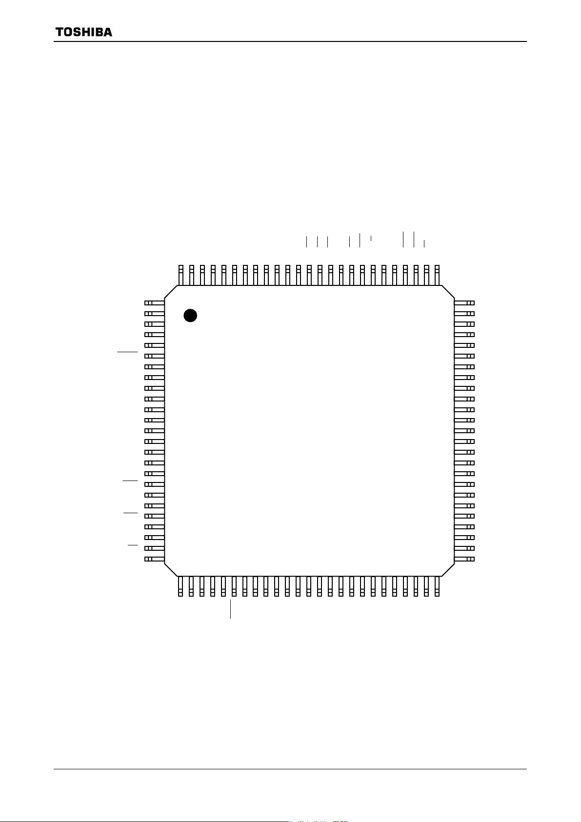
2. Pin Assignment and Functions
The assignment of input/output pins for the TMP92CM22FG, their names and functions are as
follows.
2.1 Pin Assignment
Figure 2.1.1 shows the pin assignment of the TMP92CM22FG.
TMP92CM22
VREFL
VREFH
PG0/AN0
PG1/AN1
PG2/AN2
PG3/AN3/
PC1/TA1OUT/INT1
PC5/TA3OUT/INT2
PC6/TB0OUT0/INT3
PF2/SCLK0/
PF5/SCLK1/
ADTRG
PG4/AN4
PG5/AN5
PG6/AN6
PG7/AN7
PA7
PC0/TA0IN
PF0/TXD0
PF1/RXD0
CTS0
PF3/TXD1
PF4/RXD1
CTS1
PF6
PF7
NMI
DVCC1
1
5
10
15
20
25
VCC AVSS
100
PA2
PA1
PA0
PD3/TB1OUT1
95
30
PD2/TB1OUT0
PD1/TB1IN1/INT5
PD0/TB1IN0/INT4
CS3
P90/SCK
P92/SI/SCL
P83/
P91/SO/SD
90
TMP92CM22
QFP100
Top view
35
CS2
P82/
CS1
P81/
DVSS4
85
40
CS0
P80/
WAIT
P76/
W
P74/CLKOUT
P75/R/
45
P73
80
WRLU
P72/
WRLL
P71/
RD
P70/
P67/A23
50
75
70
65
60
55
P66/A22
P65/A21
P64/A20
DVCC3
P63/A19
P62/A18
P61/A17
P60/A16
P57/A15
P56/A14
P55/A13
P54/A12
P53/A11
P52/A10
P51/A9
P50/A8
P47/A7
P46/A6
P45/A5
P44/A4
P43/A3
P42/A2
P41/A1
P40/A0
DVSS3
X1
X2
DVSS1
AM1
AM0
RESET
PC3/INT0
D0D1D2D3D4D5D6
DVSS2
DVCC2
D7
P10/D8
P11/D9
P12/D10
P13/D11
P14/D12
P15/D13
P16/D14
P17/D15
Figure 2.1.1 Pin Assignment Diagram (100-Pin QFP)
92CM22-4
2007-02-16
Page 7
2.2 Pin Names and Functions
The following tables show the names and functions of the input/output pins.
Table 2.2.1 Pin Names and Functions (1/2)
TMP92CM22
Pin Names
D0 to D7 8 I/O Data (Lower): Data bus D0 to D7.
P10 to P17
D8 to D15
P40 to P47
A0 to A7
P50 to P57
A8 to A15
P60 to P67
A16 to A23
P70
RD
P71
WRLL
P72
WRLU
P73 1 Output Port 73: Output port.
P74
CLKOUT
P75
W
R/
P76
WAIT
P80
CS0
P81
CS1
P82
CS2
P83
CS3
P90
SCK
P91
SO
SDA
P92
SI
SCL
PA0 to PA2,
PA7
Number
of Pins
8
8
8
8
1
1
1
1
1
1
1
1
1
1
1
1
1
4 Input Port A0 to A2, A7: Input port (with pull-up resistor).
I/O Functions
I/O
I/O
I/O
Output
I/O
Output
I/O
Output
Output
Output
Output
Output
Output
Output
Output
Output
Output
Output
I/O
Input
Output
Output
Output
Output
Output
Output
Output
Output
I/O
I/O
I/O
Output
I/O
I/O
Input
I/O
Port 1: I/O port that allows I/O to be selected at the bit level.
(when used to the external 8-bit bus.)
Data: Data bus D8 to D15.
Port 4: I/O port.
Address: Address bus A0 to A7.
Port 5: I/O port.
Address: Address bus A8 to A15.
Port 6: I/O port.
Address: Address bus A16 to A23.
Port 70: Output port.
Read: Strobe signal for reading external memory.
Port 71: Output port.
Write: Strobe signal for writing data to pins D0 to D7.
Port 72: Output port.
Write: Strobe signal for writing data to pins D8 to D15.
Port 74: Output port.
Clock: Output system clock.
Port 75: Output port.
Read/write: This port is 1 when read and dummy cycle. This port is 0 when write cycle.
Port 76: I/O port.
Wait: Pin used to request bus wait to CPU.
Port 80: Output port.
Chip select 0: Outputs 0 when address is within specified address area.
Port 81: Output port.
Chip select 1: Outputs 0 when address is within specified address area.
Port 82: Output port.
Chip select 2: Outputs 0 when address is within specified address area.
Port 83: Output port.
Chip select 3: Outputs 0 when address is within specified address area.
Port 90: I/O port.
Serial bus interface clock I/O data at SIO mode.
Port 91: I/O port.
Serial bus interface send data at SIO mode.
Serial bus interface send/receive data at I
(Open-drain output mode by programmable.)
Port 92: I/O port.
Serial bus interface receive data at SIO mode.
Serial bus interface clock I/O data at I
(Open-drain output mode by programmable.)
2
C mode.
2
C mode.
92CM22-5
2007-02-16
Page 8
TMP92CM22
Table 2.2.2 Pin Names and Functions (2/2)
Pin Names
Number
I/O Functions
of Pins
PC0
TA0IN
PC1
INT1
TA1OUT
PC3
INT0
PC5
INT2
TA3OUT
PC6
INT3
TB0OUT0
PD0
INT4
TB1IN0
PD1
INT5
TB1IN1
PD2
TB1OUT0
PD3
TB1OUT1
PF0
TXD0
PF1
RXD0
PF2
SCLK0
0CTS
PF3
TXD1
PF4
RXD1
PF5
SCLK1
1CTS
PF6 to PF7 2 I/O Port F6 to F7: I/O port.
PG0 to PG7
AN0 to AN7
ADTRG
NMI 1 Input Non-Maskable interrupt request pin.
AM0, AM1 2 Input
X1/X2 2 I/O High-frequency oscillator connection pin.
RESET 1 Input Reset: Initialize TMP92CM22 (Schmitt input, with pull-up resistor).
VREFH 1 Input Pin for reference voltage input to AD converter (H).
VREFL 1 Input Pin for reference voltage input to AD converter (L).
AVCC 1 Power supply pin for AD converter.
AVSS 1 GND pin for AD converter (0 V).
DVCC 3 Power supply pins (All Vcc pins should be connected with the power supply pin).
DVSS 4 − GND pins (0 V) (All DVSS pins should be connected with GND (0 V)).
1
1
1
1
1
1
1
1
1
1
1
1
1
1
1
8
I/O
Input
I/O
Input
Output
I/O
Input
I/O
Input
Output
I/O
Input
Output
I/O
Input
Input
I/O
Input
Input
I/O
Output
I/O
Output
I/O
Output
I/O
Input
I/O
I/O
Input
I/O
Output
I/O
Input
I/O
I/O
Input
Input
Input
Input
Port C0: I/O port.
Timer input: 8-bit timer A0 input.
Port C1: I/O port.
Interrupt request pin 1: Interrupt request pin with programmable level/rising edge/falling edge.
Timer output: 8-bit timer A0 or timer A1 output.
Port C3: I/O port.
Interrupt request pin 0: Interrupt request pin with programmable level/rising edge/falling edge.
Port C5: I/O port.
Interrupt request pin 2: Interrupt request pin with programmable level/rising edge/falling edge.
Timer output: 8-bit timer A2 or timer A3 output.
Port C6: I/O port.
Interrupt request pin 3: Interrupt request pin with programmable level/rising edge/falling edge.
Timer output: 16-bit timer B0 output.
Port D0: I/O port.
Interrupt request pin 4: Interrupt request pin with programmable rising edge/falling edge.
Timer input: 16-bit timer B1 input 0.
Port D1: I/O port.
Interrupt request pin 5: Interrupt request pin with programmable rising edge/falling edge.
Timer input: 16-bit timer B1 input 1.
Port D2: I/O port.
Timer output: 16-bit timer B1 output 0.
Port D3: I/O port.
Timer output: 16-bit timer B1 output 1.
Port F0: I/O port.
Serial send data 0: (Open-drain output mode by programmable.)
Port F1: I/O port.
Serial receive data 0.
Port F2: I/O port.
Serial 0 clock I/O.
Serial data send enable 0 (Clear to send).
Port F3: I/O port.
Serial send data 1: (Open-drain output mode by programmable.)
Port F4: I/O port.
Serial receive data 1.
Port F5: I/O port.
Serial 1 clock I/O.
Serial data send enable 1 (Clear to send).
Port G0 to G7: Input port.
Analog input 0 to 7: Pin used to input to AD converter.
AD trigger: Pin used to request AD converter start (Share with PG3).
Operation mode:
Fixed to AM1 = “0”, AM0 = “1”: External 16-bit bus start, 8-/16-bit dynamic sizing.
Fixed to AM1 = “1”, AM0 = “0”: External 8-bit bus start, 8-/16-bit dynamic sizing.
92CM22-6
2007-02-16
Page 9

TMP92CM22
3. Operation
This section describes the basic components, functions and operation of the TMP92CM22.
3.1 CPU
The TMP92CM22 incorporates a high-performance 32-bit CPU (The TLCS-900/H1 CPU). For
a description of this CPU’s operation, please refer to the section of this data book which
describes the TLCS-900/H1 CPU.
The following sub-sections describe functions peculiar to the CPU used in the TMP92CM22;
these functions are not covered in the section devoted to the TLCS-900/H1 CPU.
3.1.1 Outline
“TLCS-900/H1 CPU” is high-speed and high-performance CPU based on
“TLCS-900/L1 CPU”. “TLCS-900/H1 CPU” has expanded 32-bit internal and external
data bus to process instructions more quickly.
Outline of “TLCS-900/H1” CPU are as follows:
Table 3.1.1 Outline of CPU
Width of CPU address bus 24 bits
Width of CPU data bus 32 bits
Internal operating frequency 20 MHz
Minimum bus cycle 1-clock access
(50 ns at 20 MHz)
Function of data bus sizing 8 bits
Internal RAM 32 bits
1-clock access
Internal I/O 8-/16-bit 2-clock access 900/H1 I/O
8-/16-bit 5-to 6-clock access 900/H1 I/O
External device 8 bits
2-clock access (can insert some waits)
Minimum instruction execution cycle 1 clock (50 ns at 20 MHz)
Conditional jump 2 clocks (100 ns at 20 MHz)
Instruction queue buffer 12 bytes
Instruction set Compatible with TLCS-900, 900/L, 900/H, 900/L1, and 900/H2
CPU mode Only maximum mode
Micro DMA 8 channels
instruction codes (However, NORMAL, MAX, MIN, and LDX
instructions is deleted)
92CM22-7
2007-02-16
Page 10

3.1.2 Reset Operation
When resetting the TMP92CM22 microcontroller, ensure that the power supply voltage
is within the operating voltage range, and that the internal high-frequency oscillator has
stabilized. Then hold the RESET input to low for at least 20 system clocks (16 μs at fc = 40
MHz).
When the reset has been accepted, the CPU performs the following:
• Sets the program counter (PC) as follows in accordance with the reset vector stored
at address FFFF00H to FFFF02H:
• Sets the stack pointer (XSP) to 00000000H.
• Sets bits <IFF0:2> of the status register (SR) to 111 (Thereby setting the interrupt
level mask register to level 7).
• Clears bits <RFP0:1> of the status register to 00 (Thereby selecting register bank
0).
When the reset is released, the CPU starts executing instructions according to the
program counter settings. CPU internal registers not mentioned above do not change when
the reset is released.
When the reset is accepted, the CPU sets internal I/O, ports and other pins as follows.
• Initializes the internal I/O registers as “Table of Special Function Registers
(SFRs)” in Section 5.
• Sets the input or output port to general-purpose input port.
Internal reset is released as soon as external reset is released and RESET input pin is set to “H”.
The operation of memory controller cannot be insured until power supply becomes stable after power-on reset. The
external RAM data provided before turning on the TMP92CM22 may be spoiled because the control signals are
unstable until power supply becomes stable after power on reset.
Figure 3.1.1 shows the timing of a reset for the TMP92CM22.
TMP92CM22
PC<7:0> ← Data in location FFFF00H
PC<15:8> ← Data in location FFFF01H
PC<23:16> ← Data in location FFFF02H
92CM22-8
2007-02-16
Page 11
CC
TMP92CM22
3.3 V
V
RESET
operation time + 20 system clocks
Oscillator
0[s] (Min)
Figure 3.1.1 Reset Timing Example
3.1.3 Outline of Operation Mode
Set AM1 and AM0 pins to “10” to use 8-bit external bus, or set it to “01” to use 16-bit
external bus.
Table 3.1.2 Operation Mode Setup Table
Operation
16-bit external bus start
8-/16-bit dynamic bus sizing
8-bit external bus start
8-/16-bit dynamic bus sizing
Mode Setting Input Pin
RESET AM1 AM0
0 1
1 0
92CM22-9
2007-02-16
Page 12
=
3.2 Memory Map
Figure 3.2.1 shows memory map of TMP92CM22.
TMP92CM22
000000H
000100H
001FE0H
002000H
00A000H
010000H
F00000H
F10000H
FFFF00H
FFFFFFH
Internal I/O
(8 Kbytes)
Internal RAM
(32 Kbytes)
External memory
Provisinal emulator
External memory
Vector table (256 bytes)
control area
(64 Kbytes)
Direct area(n)
(
64-Kbyte area
(nn)
16-Mbyte area
(R)
( − R)
(R + )
(R + R8/16)
(R + d8/16)
Internal area)
(nnn)
Figure 3.2.1 Memory Map
Note 1: Whe n use em ulator, optional 64 Kbytes of 16-Mbyte a rea are used to control emulator.
Therefore, don’t use this area.
Note 2: Don’t use the last 16-byte area (FFFFF0H to FFFFFFH). This area is reserved.
Note 3: On emulator
WRLL signal, WRLU signal and RD signal are asserted, when provisional
emulator control area is accessed.
Be careful to use extend memory.
92CM22-10
2007-02-16
Page 13

3.3 Clock Function and Standby Function
TMP92CM22 contains (1) Clock gear, (2) Standby controller and (3) Noise-reducing circuit. It
is used for low-power, low-noise systems.
This chapter is organized as follows:
3.3.1 Block Diagram of System Clock
3.3.2 SFRs
3.3.3 System Clock Controller
3.3.4 Clock Doubler (PLL)
3.3.5 Noise Reduction Circuits
3.3.6 Standby Controller
TMP92CM22
92CM22-11
2007-02-16
Page 14
(
)
TMP92CM22
The clock operating modes are as follows: (a) Single clock mode (X1 and X2 pins only),
(b) Dual clock mode (X1, X2 pins and PLL).
Figure 3.3.1 shows a transition figure.
IDLE2 mode
(I/O operation)
IDLE1 mode
(Operate only oscillator)
IDLE2 mode
I/O operation
IDLE1 mode
(Operate only oscillator)
IDLE2 mode
(I/O operation)
IDLE1 mode
(Operate
oscillator and PLL )
Instruction
Interrupt
Instruction
Interrupt
(a) Single clock mode transition figure
Instruction
Interrupt
Instruction
Interrupt
Instruction
Interrupt
Instruction
Interrupt
(b) Dual clock mode transition figure
Reset
(f
OSCH
NORMAL mode
(f
/gear value/2)
OSCH
Reset
(f
OSCH
Release reset
NORMAL mode
(f
/gear value/2)
OSCH
NORMAL mode
(4 × f
/gear value/2)
OSCH
(Using PLL)
/32)
Release reset
/32)
Instruction
Instruction
Interrupt
Instruction
Interrupt
STOP mode
(Stop all circuit )
STOP mode
(Stop all circuit )
Figure 3.3.1 System Clock Block Diagram
The clock frequency input from the X1 and X2 pins is called f
SYSCR1<GEAR2:0> is called the clock f
one cycle of f
is defined to as one state.
SYS
. The system clock f
FPH
and the clock frequency selected by
OSCH
is defined as the divided 2 clocks of f
SYS
FPH
, and
92CM22-12
2007-02-16
Page 15
×
3.3.1 Block Diagram of System Clock
TMP92CM22
SYSCR2<WUPTM1:0>
PLLCR<PLUPFG>
Warm-up timer (for high-frequency
oscillator)/lockup (for PLL) timer
÷2
÷8
φT
φT0
f
SYS
f
iO
X1
X2
High-
frequency
oscillator
f
= f
PLL
PLLCR<PLLON>
PLL
(Clock doubler)
f
OSCH
4
OSCH
fc
PLLCR<FCSEL>
fc/2
fc/4
Clock gear
fc/8
fc/16
SYSCR1<GEAR2:0>
÷16÷8÷4÷2
f
FPH
÷2
÷4
f
SYS
φT0
f
iO
φT
TMRA0 to TMRA3 and
TMRB0 to TMRB1
Prescaler
SIO0 and SIO1
Prescaler
SBI
Prescaler
CPU
RAM
Interrupt
controller
ADC
I/O port
WDT
Figure 3.3.2 Block Diagram of Dual Clock and System Clock
92CM22-13
2007-02-16
Page 16

3.3.2 SFRs
SYSCR0
(10E0H)
SYSCR1
(10E1H)
SYSCR2
(10E2H)
Bit symbol − −
Read/Write R/W R/W
After reset 1 0
Function Always
Bit symbol − GEAR2 GEAR1 GEAR0
Read/Write R/W
After reset 0 1 0 0
Function Always
Bit symbol − WUPTM1 WUPTM0 HALTM1 HALTM0 SELDRV DRVE
Read/Write R/W R/W
After reset 0 1 0 1 1 0 0
Function Always
TMP92CM22
7 6 5 4 3 2 1 0
write “1”.
write “0”.
Always
write “0”.
Select WUP time for
oscillator
00: Reserved
8
/Input frequency
01: 2
14
/Input frequency
10: 2
16
/Input frequency
11: 2
Select HALT mode
00: Reserved
01: STOP mode
10: IDLE1 mode
11: IDLE2 mode
write “0”.
Select gear value of highfrequency oscillator
000: High-frequency oscillator
001: High-frequency oscillator/2
010: High-frequency oscillator/4
011: High-frequency oscillator/8
100: High-frequency oscillator/16
101:
110: Reserved
111:
<DRVE>
Select
using
mode
0: STOP
1: IDLE1
1: Pin
state
control
in
STOP/
IDLE1
mode
Note: The unassigned register, S YSCR0<bit6:3>, SYSCR0<bit1:0>, SYSCR1<bit7:4>, and SYSCR2<bit6> are
RD as undefined value.
Figure 3.3.3 SFR for System Clock
92CM22-14
2007-02-16
Page 17
PLLCR
(10E8H)
EMCCR0
(10E3H)
EMCCR1
(10E4H)
EMCCR2
(10E5H)
TMP92CM22
7 6 5 4 3 2 1 0
Bit symbol PLLON FCSEL LWUPFG
Read/Write R/W R
After reset 0 0 0
Function 0: PLL
stop
1: PLL
run
Note: Logic of PLLCR<LWUPFG> is different DFM of 900/L1.
0: fc =
OSCH
1: fc =
PLL (× 4)
PLL
warm-up
flag
0: Don’t
end up
or stop
1: End up
Figure 3.3.4 SFR for PLL
7 6 5 4 3 2 1 0
Bit symbol PROTECT EXTIN DRVOSCH −
Read/Write R R/W
After reset 0 0 1 1
Function Protect
0: OFF
1: ON
Bit symbol
Read/Write
After reset
Function
Bit symbol
Read/Write
After reset
Function
Note: In case restarting the oscillator in the stop oscillation state (e.g. Restart the oscillator in STOP mode), set
EMCCR0<DRVOSCH>, <DRVOSCL>= “1”.
Switching the protect ON/OFF by write to following 1st-KEY, 2nd-KEY
1st-KEY: EMCCR1 = 5AH, EMCCR2 = A5H in succession write
2nd-KEY: EMCCR1 = A5H, EMCCR2 = 5AH in succession write
1: fc
external
clock
fc oscillator
driver ability
1: Normal
0: Weak
Always
write “1”.
Figure 3.3.5 SFR for Noise
92CM22-15
2007-02-16
Page 18

3.3.3 System Clock Controller
TMP92CM22
The system clock controller generates the system clock signal (f
) for the CPU core and
SYS
internal I/O. It is used as input that fc outputted from high-frequency oscillation circuit and
PLL (Clock doubler) SYSCR1<GEAR2:0>, SYSCR1<GEAR2:0> sets the high-frequency
clock gear to either 1, 2, 4, 8, or 16 (fc, fc/2, fc/4, fc/8, or fc/16). These functions can reduce
the power consumption of the equipment in which the device is installed.
Single clock mode is set by resetting, initialized to <GEAR2:0> = “100”. This setting will
cause the system clock (f
For example, f
is set to 1.25 MHz when the 40MHz oscillator is connected to the X1
SYS
) to be set to fc/32 (fc/16×1/2).
SYS
and X2 pins.
(1) Clock gear controller
is set according to the contents of the clock gear select register
f
FPH
SYSCR1<GEAR2:0> to either fc, fc/2, fc/4, fc/8, or fc/16. Using the clock gear to select a
lower value of f
reduces power consumption.
FPH
Example:
Changing to a high-frequency gear
SYSCR1 EQU 10E1H
LD (SYSCR1), XXXX0100B ; Changes system clock f
X: Don’t care
SYS
to fc/32.
(High-speed clock gear changing)
To change the clock gear, write the register value to the SYSCR1<GEAR2:0>
register. It is necessary the warm-up time until changing after writing the register
value.
There is the possibility that the instruction next to the clock gear changing
instruction is executed by the clock gear before changing. To execute the instruction
next to the clock gear switching instruction by the clock gear after changing, input the
dummy instruction as follows (Instruction to execute the write cycle).
Example:
SYSCR1 EQU 10E1H
LD (SYSCR1), XXXX0001B ; Changes f
LD (DUMMY), 00H ; Dummy instruction.
Instruction to be executed
after clock gear has changed.
SYS
to fc/4.
92CM22-16
2007-02-16
Page 19

3.3.4 Clock Doubler (PLL)
TMP92CM22
<PLLON>
PLL outputs the f
clock signal, which is four times as fast as f
PLL
. A reset initializes
OSCH
PLL to stop status, setting to PLLCR register is needed before use.
Like an oscillator, this circuit requires time to stabilize. This is called the lockup time.
Note 1: Input frequency limitation for PLL
The limitation of input frequency (High-frequency oscillation) for PLL is the following.
f
= 4 to 10 MHz (Vcc = 3.0 V to 3.6 V)
OSCH
Note 2: PLLCR<LWUPFG>
The logic of PLLCR<LUPFG> is different from 900/L1’s DFM.
Be careful to judge an end of lockup time.
The following is a setting example for PLL starting and PLL stopping.
Example 1: PLL starting
PLLCR EQU 10E8H
LD (PLLCR), 10XXXXXXXB ; Enables PLL operation and starts lockup.
LUP: BIT 5, (PLLCR) ;
JR Z, LUP ;
LD (PLLCR), 11XXXXXXB ; Changes fc from 10 MHz to 40 MHz.
X: Don’t care
Detects end of lockup.
<FCSEL>
PLL output: f
Lockup timer
<LWUPFG>
System clock f
PLL
SYS
Count-up by f
During lockup
Starts PLL operation and
starts lockup.
OSCH
After lockup
Changes from 10 MHz to 40 MHz.
Ends of lockup
92CM22-17
2007-02-16
Page 20
<FCSEL>
<PLLON>
PLL output: f
System clock f
Example 2: PLL stopping
PLLCR EQU 10E8H
LD (PLLCR), 10XXXXXXB ; Changes fc from 40 MHz to10 MHz.
LD (PLLCR), 00XXXXXXB ; Stop PLL.
X: Don’t care
PLL
SYS
Changes from 40 MHz to 10 MHz.
Stops PLL
operation.
TMP92CM22
Limitation point on the use of PLL
1. When PLL is started, don’t set fc from f
Don’t setting:
LD (PLLCR), 00H
LD (PLLCR), C0H
2. When PLL is started, don’t set fc from f
Don’t setting:
LD (PLLCR), C0H
LD (PLLCR), 00H
OSCH
OSCH
to f
to f
at same time.
PLL
at same time.
PLL
92CM22-18
2007-02-16
Page 21
3.3.5 Noise Reduction Circuits
Noise reduction circuits are built in for reduction EMI (Unnecessary radius noise) and
reinforcement EMS (Measure of endure noise), allowing implementation of the following
features.
(1) Reduced drivability for high-frequency oscillator
(2) Single drive for high-frequency oscillator
(3) SFR protection of register contents
These functions need setting by EMCCR0 to EMCCR2.
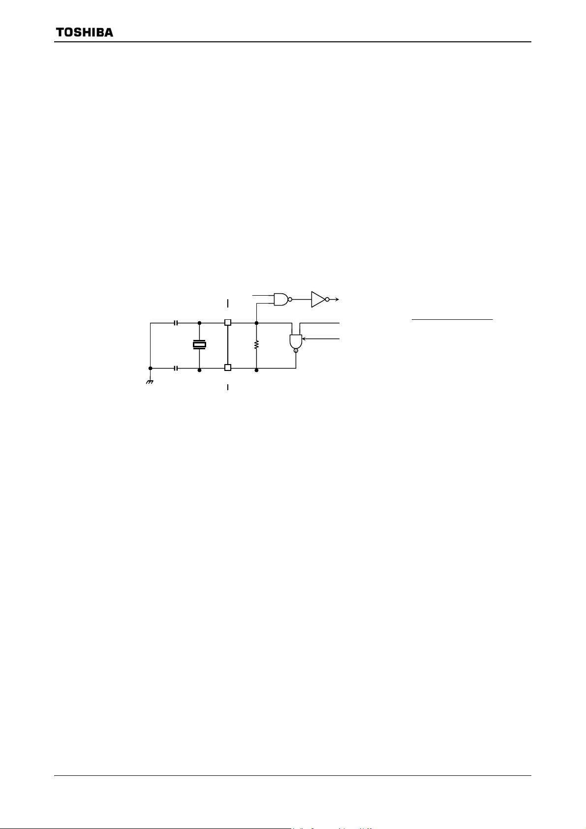
(1) Reduced drivability for high-frequency oscillator
(Purpose)
Reduces noise and power for oscillator when connect oscillator to outside.
(Block diagram)
C1
Oscillator
C2
(Setting method)
X1 pin
X2 pin
f
OSCH
Oscillation enable (
EMCCR0<DRVOSCH>
TMP92CM22
)
><+ EXTINEMCCR0STOP
The drivability of the oscillator is reduced by writing “0” to
EMCCR0<DRVOSCH> register. By reset, <DRVOSCH> is initialized to “1” and
the oscillator starts oscillation by normal drivability when the power supply is on.
Note: When use drivability reduction function of oscillator, please use in case of
= 4 MHz to 10 MHz condition.
f
OSCH
92CM22-19
2007-02-16
Page 22
TMP92CM22
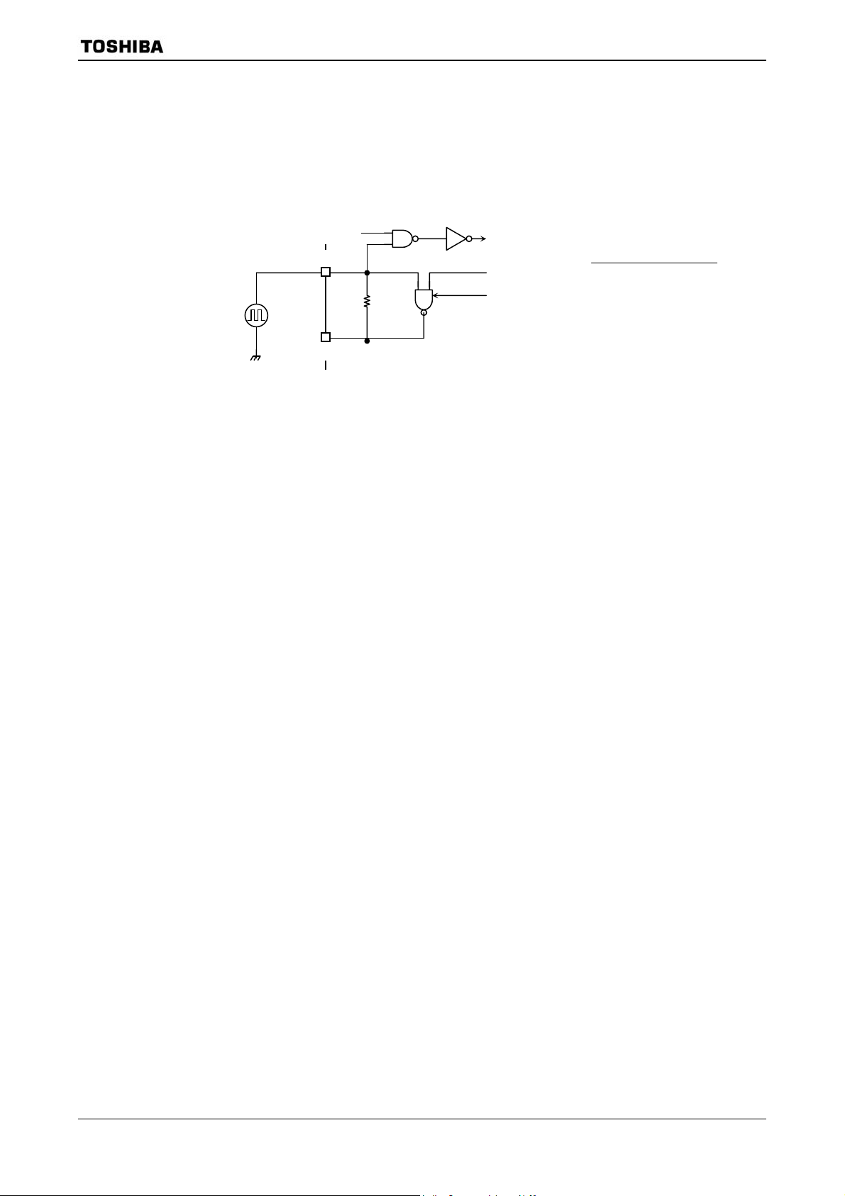
(2) Single drive for high-frequency oscillator
(Purpose)
Not need twin-drive and protect mistake operation by inputted noise to X2 pin
when the external oscillator is used.
(Block diagram)
f
X1 pin
X2 pin
OSCH
Oscillation enable (
EMCCR0<DRVOSCH>
><+ EXTINEMCCR0STOP )
(Setting method)
The oscillator is disabled and starts operation as buffer by writing “1” to
EMCCR0<EXTIN> register. X2 pin is always outputted “1”.
By reset, <EXTIN> is initialized to “0”.
92CM22-20
2007-02-16
Page 23

TMP92CM22
(3) Runaway provision with SFR protection register
(Purpose)
Provision in runaway of program by noise mixing.
Write operation to specified SFR is prohibited so that provision program in
runaway prevents that is in the state which is fetch impossibility by stopping of
clock, memory control register (Memory controller) is changed.
And error handling in runaway becomes easy by INTP0 interruption.
Specified SFR list
1. Memory controller
B0CSL/H, B1CSL/H, B2CSL/H, B3CSL/H, BEXCSL/H,
MSAR0, MSAR1, MSAR2, MSAR3,
MAMR0, MAMR1, MAMR2, MAMR3, and PMEMCR
2. Clock gear (EMCCR1, EMCCR2 write enable)
SYSCR0, SYSCR1, SYSCR2, and EMCCR0
(Operation explanation)
Execute and release of protection (write operation to specified SFR) becomes
possible by setting up a double key to EMCCR1 and EMCCR2 registers.
(Double key)
1st-KEY: Succession writes in 5AH at EMCCR1 and A5H at EMCCR2.
2nd-KEY: Succession writes in A5H at EMCCR1 and 5AH at EMCCR2.
A state of protection can be confirmed by reading EMCCR0<PROTECT>.
By reset, protection becomes OFF.
And INTP0 interruption occurs when write operation to specified SFR was
executed with protection on state.
92CM22-21
2007-02-16
Page 24

3.3.6 Standby Controller
(1) HALT modes
When the HALT instruction is executed, the operating mode switches to IDLE2,
IDLE1, or STOP mode, depending on the contents of the SYSCR2<HALTM1:0>
register.
The subsequent actions performed in each mode are as follows:
a. IDLE2: Only the CPU halts.
The internal I/O is available to select operation during IDLE2 mode by setting the
following register.
Table 3.3.1 shows the registers of setting ope ration during IDLE2 mode.
Table 3.3.1 SFR Seting Operation during IDLE2 Mode
b. IDLE1: Only internal oscillator operates.
c. STOP: All internal circuit stop.
Internal I/O SFR
TMRA01 TA01RUN<I2TA01>
TMRA23 TA23RUN<I2TA23>
TMRB0 TB0RUN<I2TB0>
TMRB1 TB1RUN<I2TB1>
SIO0 SC0MOD1<I2S0>
SIO1 SC1MOD1<I2S1>
AD converter ADMOD1<I2AD>
WDT WDMOD<I2WDT>
SBI SBI0BR0<I2SBI0>
The operation of each of the different HALT modes is described in
TMP92CM22
Table 3.3.2.
Table 3.3.2 Each Block Operation in HALT Mode
HALT Mode IDLE2 IDLE1 STOP
SYSCR2<HALTM1:0> 11 10 01
CPU Stop
I/O port Keep the state when the HALT
TMRA, TMRB
SIO, *SBI
AD converter
Operation block
WDT
instruction is executed.
* Selection enable operation
block to programmable
*: Except clocked-synchronous 8 -bit SIO mode for SBI.
Refer
Table 3.3.5, Table 3.3.6
Stop
92CM22-22
2007-02-16
Page 25

(2) How to release the HALT mode
These halt states can be released by resetting or requesting an interrupt. The halt
release sources are determined by the combination between the states of interrupt
mask register <IFF2:0> and the HALT modes. The details for release the halt status
are shown in
• Released by requesting an interrupt
The operating released from the HALT mode depends on the interrupt enabled
status. When the interrupt request level set before executing the HALT
instruction exceeds the value of interrupt mask register, the interrupt due to the
source is processed after release the HALT mode, and CPU status executing an
instruction that follows the HALT instruction. When the interrupt request level
set before executing the HALT instruction is less than the value of the interrupt
mask register, release the HALT mode is not executed. (In non-maskable
interrupts, interrupt processing is processed after release the HALT mode
regardless of the value of the mask register.) However only for INT0 to INT3
interrupts, even if the interrupt request level set before executing the HALT
instruction is less than the value of the interrupt mask register, release the HALT
mode is executed. In this case, interrupt processing, and CPU starts executing the
instruction next to the HALT instruction, but the interrupt request flag is held at
“1”.
Table 3.3.3.
TMP92CM22
• Release by resetting
Release all halt status is executed by resetting.
When the STOP mode is released by RESET, it is necessary enough resetting
time (Refer
When release the HALT mode by resetting, the internal RAM data keeps the
state before the “HALT” instruction is executed. However the other settings
contents are initialized. (Release due to interrupts keeps the state before the
“HALT” instruction is executed.)
Table 3.3.4) to set the operation of the oscillator to be stable.
92CM22-23
2007-02-16
Page 26
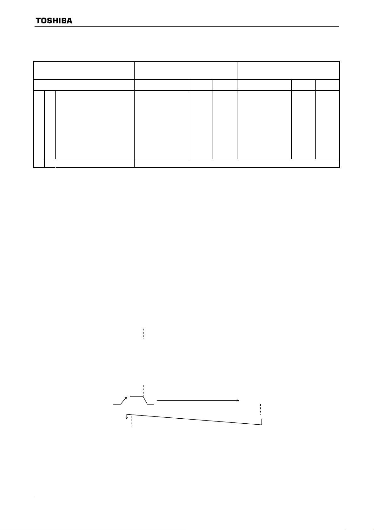
Table 3.3.3 Source of Halt State Release and Halt Release Operation
TMP92CM22
Status of Received Interrupt
Interrupt Enable
(Interrupt level) ≥ (Interrupt mask)
Interrupt Disable
(Interrupt level) < (Interrupt mask)
HALT Mode Programmable IDLE2 IDLE1 STOP Programmable IDLE2 IDLE1 STOP
NMI
INTWDT
INT0 to 3 (Note1)
INT4 to 5
INTTA0 to 3,
Interrupt
INTTB00, 01, 10, 11, O0, O1
INTRX0 to 1, TX0 to 1
INTAD
INTSBE0
Source of HALT state release
Reset Initialize LSI
♦
♦
♦
♦
♦
♦
♦
♦
♦
♦
♦
♦
×
×
×
×
×
×
×
×
♦*1
×
×
×
×
×
×
−
−
○
×
×
×
×
×
×
−
−
○
×
×
×
×
×
×
♦: After release the HALT mode, CPU starts interrupt processing.
○: After release the HALT mode, CPU resumes executing starting from instruction following the HALT
instruction. (Interrupt don’t process.)
×: It can not be used to release the HALT mode.
−: The priority level (Interrupt request level) of non-maskable interrupts is fixed to 7, the highest priority
level. There is not this combination type.
−
−
○*1
×
×
×
×
×
×
*1: Release the HALT mode is executed after passing the warm-up time.
Note 1: When the HALT mode is released by INT0 to INT3 interrupts of the level mode in the interrupt
enabled status, hold this level until starting interrupt pro cessing. Changing level before holding level,
interrupt processing is correctly started.
Note 2: When use external interrupt INT4 to INT5 are used during IDLE2 mode, set 16-bit timer RUN
register TB1RUN<I2TB1> to “1”.
(Example release HALT mode)
An INT0 interrupt release the halt state when the device is in IDLE1 mode.
Address
8203H LD (IIMC), 00H ; Selects INT0 interrupt rising edge.
8206H LD (INTE0AD), 06H ; Sets INT0 interrupt level to 6.
8209H EI 5 ; Sets CPU interrupt level to 5.
820BH LD (SYSCR2), 28H ; Sets HALT mode to IDLE1 mode.
820EH HALT ; Halts CPU.
INT0 INT0 interrupt routine
RETI
820FH LD XX, XX
92CM22-24
2007-02-16
Page 27
f
f
TMP92CM22
(3) Operation
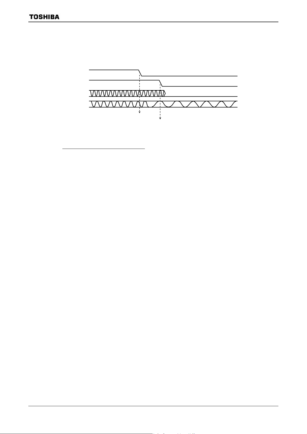
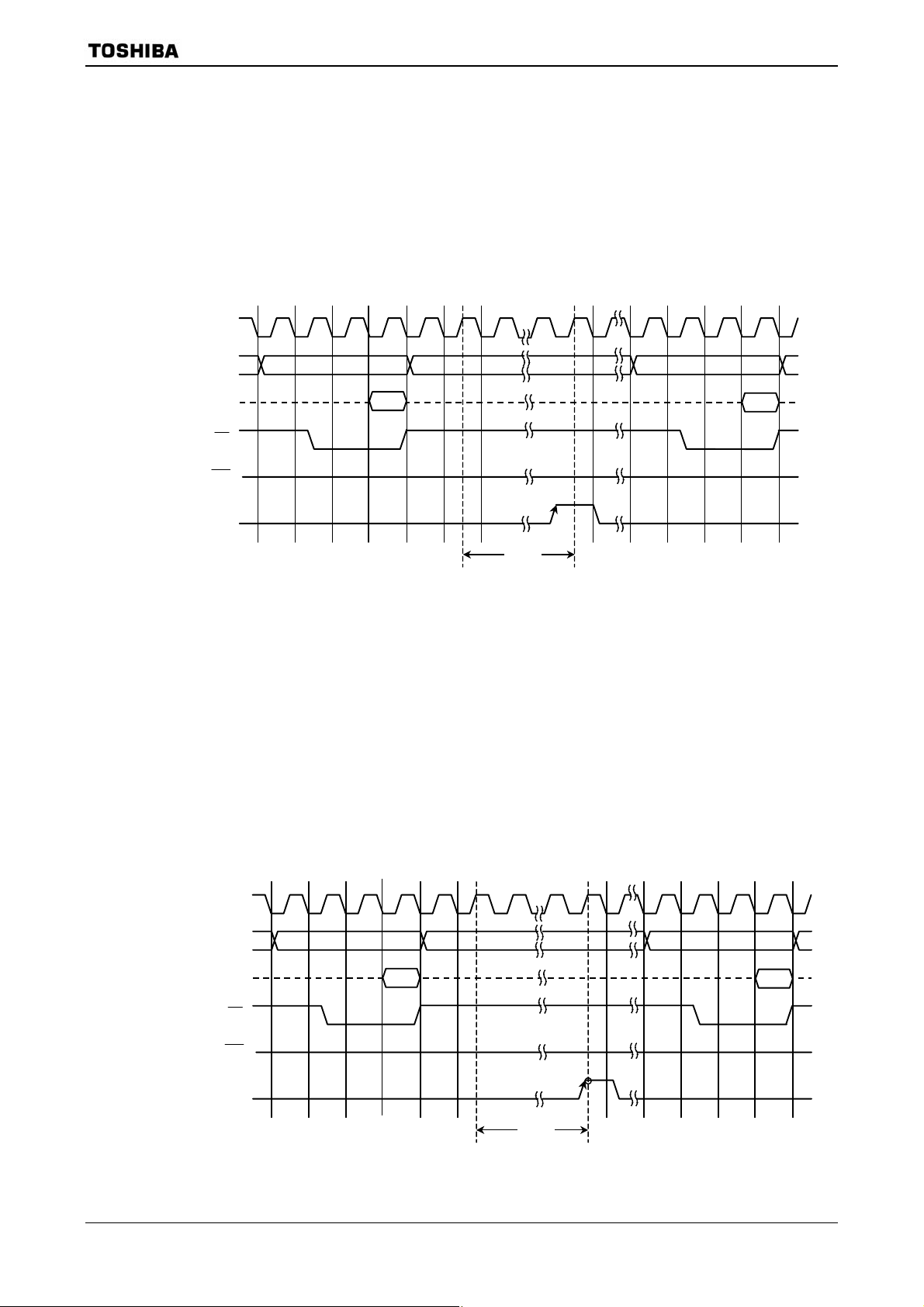
a. IDLE2 mode
In IDLE2 mode only specific internal I/O operations, as designated by the
IDLE2 setting register, can take place. Instruction execution by the CPU stops.
Figure 3.3.6 illustrates an example of the timing for clearance of the IDLE2
mode halt state by an interrupt.
X1
A0 to A23
D0 to D15
RD
WR
Interrupt o
releasing halt
Data
Data
IDLE2
mode
Figure 3.3.6 Timing Chart for IDLE2 Mode Halt State Released by Interrupt
b. IDLE1 mode
In IDLE1 mode, only the internal oscillator operates. The system clock stops.
And, pin state in IDLE1 mode depend on setting SYSCR2<SELDRV, DRVE>
register.
Table 3.3.5, Table 3.3.6 shows pin state in IDLE1 mode.
In the halt state, the interrupt request is sampled asynchronously with the
system clock; however, clearance of the halt state (e.g., restart of operation) is
synchronous with it.
Figure 3.3.7 shows the timing for release of the IDLE1 mode halt state by an
interrupt.
X1
A0 to A23
D0 to D15
RD
WR
Interrupt o
releasing halt
Data
Data
IDLE1
mode
Figure 3.3.7 Timing Chart for IDLE1 Mode Halt State Released by Interrupt
92CM22-25
2007-02-16
Page 28

f
TMP92CM22
c. STOP mode
When STOP mode is selected, all internal circuits stop, including the internal
oscillator pin status in STOP mode depends on the settings in the
SYSCR2<SELDRV, DRVE> register.
Table 3.3.5, Table 3.3.6 shows the state of
these pins in STOP mode.
After STOP mode has been released system clock output starts when the
warm-up time has elapsed, in order to allow oscillation to stabilize. Warm-up time
set by SYSCR2<WUPTM1:0> register. See the sample warm-up times in
Table
3.3.4.
Figure 3.3.8 illustrates the timing for release of the STOP mode halt state by an
interrupt.
War m -up time
X1
A0 to A23
D0 to D15
RD
WR
Interrupt o
releasing halt
Data Data
STOP
mode
Figure 3.3.8 Timing Chart for STOP Mode Halt State Released by Interrupt
Table 3.3.4 Sample Warm-up Times after Rrelease of STOP Mode
at f
OSCH
= 10 MHz
SYSCR2<WUPTM1:0>
01 (28) 10 (214) 11 (216)
25.6 μs 1.638 ms 6.554 ms
92CM22-26
2007-02-16
Page 29

TMP92CM22
Table 3.3.5 Input Buffer State Table
Input Buffer State
Port
Name
D0-D7 D0-D7 − − − −
P10-P17 D8-D15
Input
Function
Name
During
Reset
OFF
P40-P47 −
P50-P57 −
P60-P67 −
P76 WAIT OFF
P90 SCK
P91 SDA
P92
PA0-PA7(*1) − − − ON − ON − ON
PC0 TA0IN OFF OFF
PC1 INT1
PC3 INT0 ON ON ON
PC5 INT2
PC6 INT3
PD0
PD1
PD2 −
PD3 −
PF0 −
PF1 RXD0
PF2
PF3 − − − OFF − −
PF4 RXD1
PF5
PF6 −
PF7 −
PG0-2,
PG4-7(*2)
PG3(*2) ADTRG
−
NMI
RESET(*1) −
AM0,1 −
X1
SI
SCL
INT4,
TB1IN0
INT5,
TB1IN1
SCLK0,
CTS0
SCLK1,
CTS1
−
ON
OFF
ON
ON: The buffer is always turned on. A current flows
Input Buffer State Input Buffer State
When
Used as
function
Pin
When
Used as
Input
Port
When
Used as
function
Pin
When
Used as
Input
Port
ON
upon
external
OFF OFF OFF
read
− − − −
OFF
ON
ON
OFF OFF OFF
ON ON
ON
OFF
− −
ON ON ON OFF OFF
ON ON OFF OFF
ON
− − − −
ON
upon
port
OFF
read
ON
−
ON
−
*1: Port having a pull-up/pull-down resistor.
the input buffer if the input pin is not driven.
OFF: The buffer is always turned off.
*2: AIN input does not cause a current to flow through the
buffer.
−: No applicable
In HALT mode (IDLE1/STOP)
Condition A (Note) Condition B (Note)
When
Used as
function
Pin
OFF
When
Used as
Input
Port
OFF
When
Used as
function
Pin
OFF
When
Used as
Input
Port
OFF
ON ON
OFF OFF
− −
OFF OFF
ON
−
ON
−
Note: Condition A/B are as follows.
SYSCR2 register setting HALT mode
<DRVE> <SELDRV> IDLE1 STOP
0 0 Condition B
0 1 Condition A
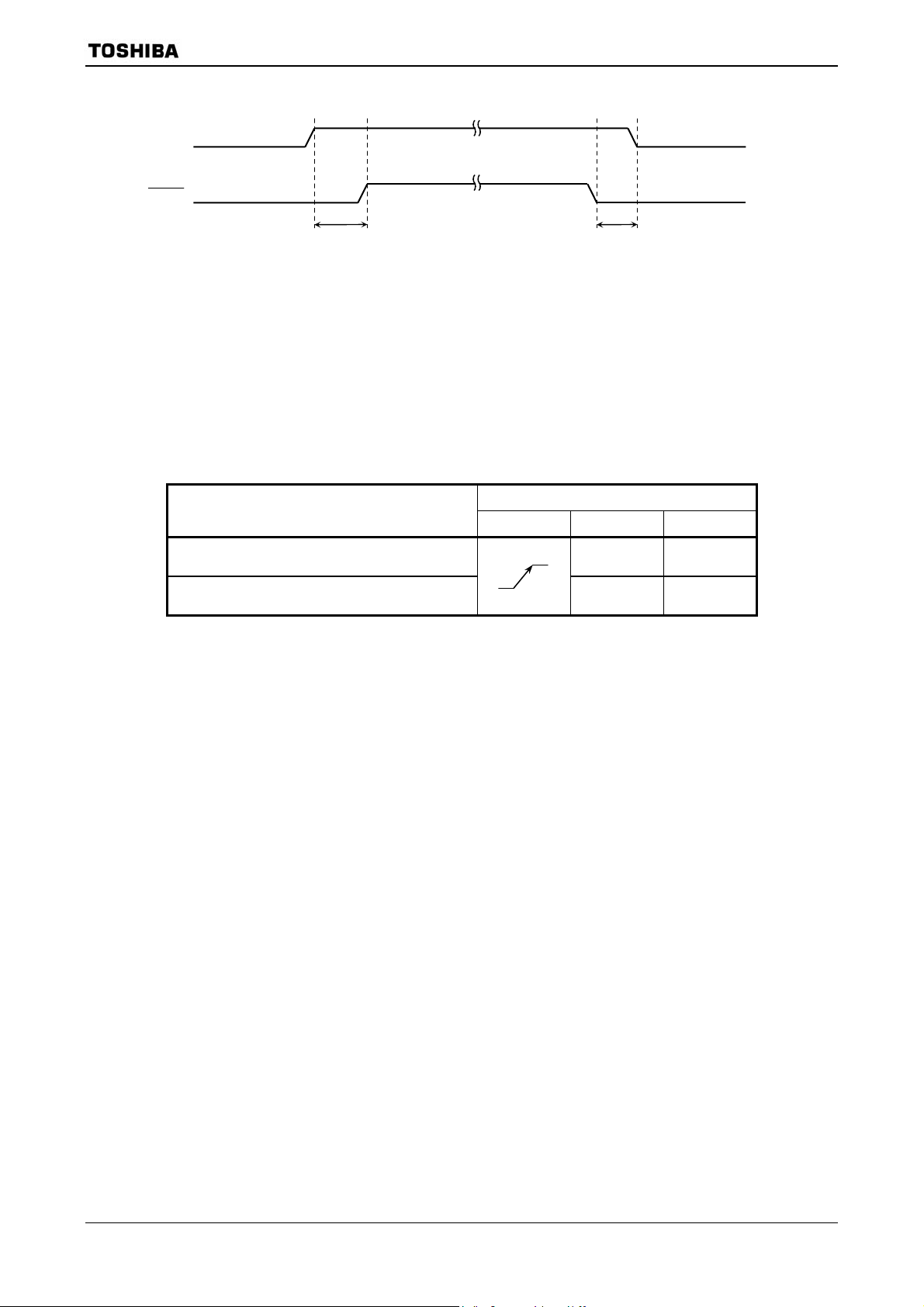
1 0
1 1
Condition A
Condition B Condition B
92CM22-27
2007-02-16
Page 30
TMP92CM22
Table 3.3.6 Output Buffer State Table
Output Buffer State
Port
Name
D0-D7 D0-D7 − − − −
P10-P17 D8-D15
P40-P47 A0-A7
P50-P57 A8-A15
P60-P67 A16-A23
P70
P71 WRLL
P72 WRLU
P73 WRUL
P74 WRUU
P75 R/W
P76 − OFF − − − −
P80 CS0
P81 CS1
P82 CS2
P83 CS3
P90 SCK
P91 SO
P92 SCL
PC0 − − − − −
PC1 TA1OUT ON ON OFF ON
PC3 − − − − −
PC5 TA3OUT
PC6 TB0OUT
PD0 −
PD1 −
PD2 TB1OUT0 ON
PD3 TB1OUT1
PF0 TXD0 ON
PF1 − − − − −
PF2 SCLK0
PF3 TXD1
PF4 − − − − −
PF5 SCLK1 ON ON OFF ON
PF6 −
PF7 −
X2 − − ON − IDLE1: ON, STOP: High level output
Note: Condition A/B are as follows.
Output
Function
Name
RD
ON: The buffer is always turned on. When the bus is released,
however ,output buffers for some pins are turned off.
OFF: The buffer is always turned off.
−: No applicable
SYSCR2 register setting HALT mode
<DRVE> <SELDRV> IDLE1 STOP
0 0 Condition B
0 1 Condition A
1 0
1 1
During
Reset
OFF
ON ON ON
ON
OFF
When the CPU is
Operating
When
Used as
Function
Pin
ON upon
external
read
ON ON OFF ON
ON ON OFF ON
− − − −
ON ON OFF ON
−
When
Used as
Output
Port
Condition B Condition B
ON
In HALT
mode(IDLE2)
When
Used as
Function
Pin
OFF
ON OFF ON
−
Condition A
When
Used as
Output
Port
ON
Used as
Function
In HALT mode (IDLE1/STOP)
Condition A (Note) Condition B (Note)
When
Pin
OFF
−
When
Used as
Output
Port
ON
OFF
When
Used as
Function
Pin
OFF
ON
−
When
Used as
Output
Port
ON
92CM22-28
2007-02-16
Page 31

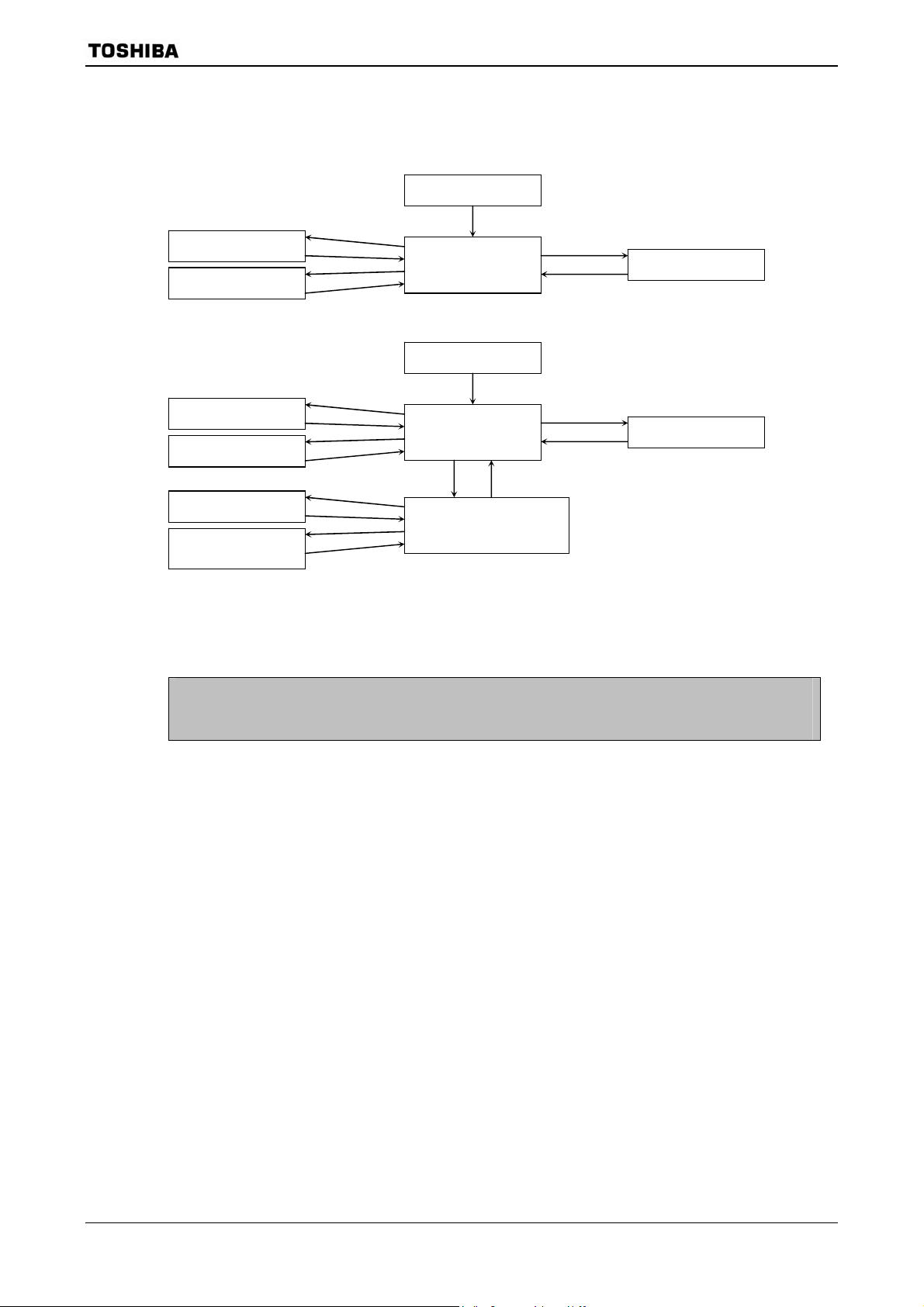
3.4 Interrupt
Interrupts of TLCS-900/H1 are controlled by the CPU interrupt mask flip-flop (IFF2:0) and
by the built-in interrupt controller.
The TMP92CM22 has a total of 41 interrupts divided into the following types:
Interrupts generated by CPU: 9 sources
External interrupts (
Internal I/O interrupts: 17 sources
High-speed DMA interrupts: 8 sources
A individual interrupt vector number (Fixed) is assigned to each interrupt.
One of six priority level (Variable) can be assigned to each maskable interrupt.
The priority level of non-maskable interrupts are fixed at 7 as the highest level.
When an interrupt is generated, the interrupt controller sends the priority of that interrupt
to the CPU. If multiple interrupts is generated simultaneously, the interrupt controller sends
the interrupt with the highest priority to the CPU. (The highest priority is level 7 using for
non-maskable interrupts.)
The CPU compares the priority level of the interrupt with the value of the CPU interrupts
mask register <IFF2:0>. If the priority level of the interrupt is higher than the value of the
interrupt mask register, the CPU accepts the interrupt.
The interrupt mask register <IFF2:0> value can be updated using the value of the EI
instruction (EI num sets <IFF2:0> data to num).
For example, specifying “EI3” enables the maskable interrupts which priority level set in the
interrupt controller is 3 or higher, and also non-maskable interrupts.
Operationally, the DI instruction (<IFF2:0> = 7) is identical to the EI7 instruction. DI
instruction is used to disable maskable interrupts because of the priority level of maskable
interrupts is 1 to 6. The EI instruction is valid immediately after execution.
In addition to the above general-purpose interrupt processing mode, TLCS-900/H1 has a
micro DMA interrupt processing mode as well. The CPU can transfer the data (1/2/4 bytes)
automatically in micro DMA mode, therefore this mode is used for speed-up interrupt
processing, such as transferring data to the internal or external peripheral I/O. Moreover,
TMP92CM22 has software start function for micro DMA processing request by the software not
by the hardware interrupt.
Figure 3.4.1 shows the overall interrupt processing flow.
TMP92CM22
(Software interrupts: 8 sources, illegal instruction interrupt: 1 source)
NMI and INT0 to INT5): 7 sources
92CM22-29
2007-02-16
Page 32

+
r
TMP92CM22
Interrupt processing
Interrupt
specified by
micro DMA start
vector?
No
Yes
Clear interrupt request flag
Micro DMA
soft start request
General-purpose
interrupt
processing
Interrupt vector “V” read
Interrupt request F/F clear
PUSH PC
PUSH SR
SR<IFF2:0> ← Level of
accepted
interrupt + 1
INTNEST ← INTNEST
PC←(FFFF00H) + V)
Interrupt process
program
RETI instruction
POP SR
POP PC
INTNEST ← INTNEST−1
End
Data transfer by
micro DMA
COUNT ← COUNT − 1
1
COUNT = 0
No
Micro DMA processing
Generating INTTC
Yes
interrupt
clear micro DMA start
vecto
Figure 3.4.1 Interrupt and Micro DMA Processing Sequence
92CM22-30
2007-02-16
Page 33

3.4.1 General-purpose Interrupt Processing
When the CPU accepts an interrupt, it usually performs the following sequence of
operations. That is also the same as TLCS-900/L, TLCS-900/H, and TLCS-900/L1.
(1) The CPU reads the interrupt vector from the interrupt controller.
If the same level interrupts occur simultaneously, the interrupt controller generates an
interrupt vector in accordance with the default priority and clears the interrupt
request.
(The default priority is already fixed for each interrupt: The smaller vector value has
the higher priority level.)
(2) The CPU pushes the value of program counter (PC) and status register (SR) onto the
stack area (indicated by XSP).
(3) The CPU sets the value which is the priority level of the accepted interrupt plus 1 (+1)
to the interrupt mask register <IFF2:0>. However, if the priority level of the accepted
interrupt is 7, the register’s value is set to 7.
(4) The CPU increases the interrupt nesting counter INTNEST by 1 (+1).
TMP92CM22
(5) The CPU jumps to the address indicated by the data at address “FFFF00H + Interrupt
vector” and starts the interrupt processing routine.
When the CPU completed the interrupt processing, use the RETI instruction to return to
the main routine. RETI restores the contents of program counter (PC) and status register
(SR) from the stack and decreases the interrupt nesting counter INTNEST by 1(−1).
Non-maskable interrupts cannot be disabled by a user program. Maskable interrupts,
however, can be enabled or disabled by a user program. A program can set the priority level
for each interrupt source. (A priority level setting of 0 or 7 will disable an interrupt
request.)
If an interrupt request which has a priority level equal to or greater than the value of the
CPU interrupt mask register <IFF2:0> comes out, the CPU accepts its interrupt. Then, the
CPU interrupt mask register <IFF2:0> is set to the value of the priority level for the
accepted interrupt plus 1(+1).
Therefore, if an interrupt is generated with a higher level than the current interrupt
during it’s processing, the CPU accepts the later interrupt and goes to the nesting status of
interrupt processing.
Moreover, if the CPU receives another interrupt request while performing the said (1) to
(5) processing steps of the current interrupt, the latest interrupt request is sampled
immediately after execution of the first instruction of the current interrupt processing
routine. Specifying DI as the start instruction disables maskable interrupt nesting.
A reset initializes the interrupt mask register <IFF2:0> to “7”, disabling all maskable
interrupts.
Table 3.4.1 shows the TMP92CM22 interrupt vectors and micro DMA start vectors. The
address FFFF00H to FFFFFFH (256 bytes) is assigned for the interrupt vector area.
92CM22-31
2007-02-16
Page 34

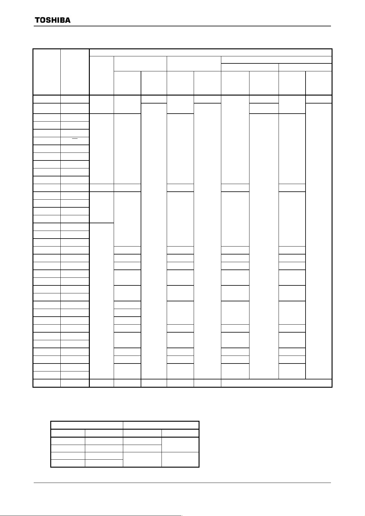
Table 3.4.1 TMP92CM22 Interrupt Vectors and Micro DMA Start Vectors
TMP92CM22
Default Priority
1 Reset or “SWI0” instruction 0000H FFFF00H
2 “SWI1” instruction 0004H FFFF04H
3 “Illegal instruction” or “SWI2” instruction 0008H FFFF08H
4 “SWI3” instruction 000CH FFFF0CH
5 “SWI4” instruction 0010H FFFF10H
6 “SWI5” instruction 0014H FFFF14H
7 “SWI6” instruction 0018H FFFF18H
8 “SWI7” instruction 001CH FFFF1CH
9 NMI: External interrupt input pin 0020H FFFF20H
10
- Micro DMA (Note 2) − − −
11 INT0: External interrupt input pin 0028H FFFF28H 0AH (Note 1)
12 INT1: External interrupt input pin 002CH FFFF2CH 0BH (Note 1)
13 INT2: External interrupt input pin 0030H FFFF30H 0CH (Note 1)
14 INT3: External interrupt input pin 0034H FFFF34H 0DH (Note 1)
15 (Reserved) 0038H FFFF38H 0EH
16 (Reserved) 003CH FFFF3CH 0FH
17 (Reserved) 0040H FFFF40H 10H
18 (Reserved) 0044H FFFF44H 11H
19 (Reserved) 0048H FFFF48H 12H
20 (Reserved) 004CH FFFF4CH 13H
21 INTP0: Protect 0 (WR to SFR) 0050H FFFF50H 14H
22 (Reserved) 0054H FFFF54H 15H
23 INTTA0: 8-bit timer 0 0058H FFFF58H 16H
24 INTTA1: 8-bit timer 1 005CH FFFF5CH 17H
25 INTTA2: 8-bit timer 2 0060H FFFF60H 18H
26 INTTA3: 8-bit timer 3 0064H FFFF64H 19H
27 INTTB00: 16-bit timer 0 0068H FFFF68H 1AH
28 INTTB01: 16-bit timer 0 006CH FFFF6CH 1BH
29 (Reserved) 0070H FFFF70H 1CH
30 (Reserved) 0074H FFFF74H 1DH
31 INTTBO0: 16-bit timer 0 (Overflow) 0078H FFFF78H 1EH
32 (Reserved) 007CH FFFF7CH 1FH
33 INTRX0: Serial 0 (SIO0) receive 0080H FFFF80H 20H (Note 1)
34 INTTX0: Serial 0 (SIO0) transmission 0084H FFFF84H 21H
35 INTRX1: Serial 1 (SIO1) receive 0088H FFFF88H 22H (Note 1)
36 INTTX1: Serial 1 (SIO1) transmission 008CH FFFF8CH 23H
37 (Reserved) 0090H FFFF90H 24H
38 (Reserved) 0094H FFFF94H 25H
39 (Reserved) 0098H FFFF98H 26H
40 (Reserved) 009CH FFFF9CH 27H
41 (Reserved) 00A0H FFFFA0H 28H
42 INT4: External interrupt input pin 00A4H FFFFA4H 29H
43 INT5: External interrupt input pin 00A8H FFFFA8H 2AH
44 INTTB10: 16-bit timer 1 00ACH FFFFACH 2BH
45 INTTB11: 16-bit timer 1 00B0H FFFFB0H 2CH
46 INTTBO1: 16-bit timer 1 (Overflow) 00B4H FFFFB4H 2DH
47 (Reserved) 00B8H FFFFB8H 2EH
48 INTSBE0: SBI I2C bus transfer end (Channel 0) 00BCH FFFFBCH 2FH
49 (Reserved) 00C0H FFFFC0H 30H
50 (Reserved) 00C4H FFFFC4H 31H
51
Type Interrupt Source
Non-
maskable
INTWD: Watchdog Timer 0024H FFFF24H
Maskable
(Reserved) 00C8H FFFFC8H 32H
Vector
Value
Address
Refer to
Vector
Micro DMA
Start Vector
92CM22-32
2007-02-16
Page 35

TMP92CM22
Default Priority
52 INTAD: AD conversion end 00CCH FFFFCCH 33H
53 INTTC0: Micro DMA end (Channel 0) 00D0H FFFFD0H 34H
54 INTTC1: Micro DMA end (Channel 1) 00D4H FFFFD4H 35H
55 INTTC2: Micro DMA end (Channel 2) 00D8H FFFFD8H 36H
56 INTTC3: Micro DMA end (Channel 3) 00DCH FFFFDCH 37H
57 INTTC4: Micro DMA end (Channel 4) 00E0H FFFFE0H 38H
58 INTTC5: Micro DMA end (Channel 5) 00E4H FFFFE4H 39H
59 INTTC6: Micro DMA end (Channel 6) 00E8H FFFFE8H 3AH
60 INTTC7: Micro DMA end (Channel 7) 00ECH FFFFECH 3BH
Type Interrupt Source
Maskable
(Reserved)
Note 1 : When initiating initiating micro DMA, set at edge detect mode.
Note 2 : Micro DMA default priority.
Micro DMA initiation takes priority over other maskable interrupts
Vector
Value
00F0H
:
00FCH
Address
Refer to
Vector
FFFFF0H
:
FFFFFCH
Micro DMA
Start Vector
−
92CM22-33
2007-02-16
Page 36

3.4.2 Micro DMA
In addition to general-purpose interrupt processing, the TMP92CM22 also includes a
micro DMA function. Micro DMA processing for interrupt requests set by micro DMA is
performed at the highest priority level for maskable interrupts (Level 6), regardless of the
priority level of the interrupt source.
Because the micro DMA function is implemented through the CPU, when the CPU is
placed in a stand-by state by a Halt instruction, the requirements of the micro DMA will be
ignored (pending).
Micro DMA is supports 8 channels and can be transferred continuously by specifying the
micro DMA burst function as below.
(1) Micro DMA operation
DMA start vector register, the micro DMA triggers a micro DMA request to the CPU at
interrupt priority level 6 and starts processing the request. The eight micro DMA
channels allow micro DMA processing to be set for up to eight types of interrupt at
once.
channel is cleared. Data in one-byte, two-byte or four-byte blocks, is automatically
transferred at once from the transfer source address to the transfer destination
address set in the control register, and the transfer counter is decremented by 1. If the
value of the counter after it has been decremented is not 0, DMA processing ends with
no change in the value of the micro DMA start vector register. If the value of the
decremented counter is 0, a micro DMA transfer end interrupt (INTTC0 to INTTC7) is
sent from the CPU to the interrupt controller. In addition, the micro DMA start vector
register is cleared to 0, the next micro DMA operation is disabled and micro DMA
processing terminates.
not based on the interrupt priority level but on the channel number: the lower the
channel number, the higher the priority (channel 0 thus has the highest priority and
channel 7 the lowest).
between the time at which the micro DMA start vector is cleared and the next setting,
general purpose interrupt processing is performed at the interrupt level set. Therefore,
if the interrupt is only being used to initiate micro DMA (and not as a general-purpose
interrupt), the interrupt level should first be set to 0 (i.e., interrupt requests should be
disabled).
TMP92CM22
When an interrupt request is generated by an interrupt source specified by the micro
When micro DMA is accepted, the interrupt request flip-flop assigned to that
If micro DMA requests are set simultaneously for more than one channel, priority is
If an interrupt request is triggered for the interrupt source in use during the interval
If micro DMA and general purpose interrupts are being used together as described
above, the level of the interrupt which is being used to initiate micro DMA processing
should first be set to a lower value than all the other interrupt levels. (Note) In this
case, edge triggered interrupts are the only kinds of general interrupts which can be
accepted.
Note: If the priority level of micro DMA is set higher than that of other interrupts, CPU operates as follows.
In case INTxxx interrupt is generated first and then INTyyy interrupt is generated between checking
“Interrupt specified by micro DMA start vector” (in the
setting below. The vector shifts to that of INTyyy at the time.
This is because the priority level of INTyyy is higher than that of INTxxx.
In the interrupt routine, CPU reads the vector of INTyyy because cheking of micro DMA has finished.
And INTyyy is generated regardless of transfer counter of micro DMA.
INTxxx: level 1 without micro DMA
INTyyy: level 6 with micro DMA
92CM22-34
Figure 3.4.1) and reading interrupt vector with
2007-02-16
Page 37

TMP92CM22
Although the control registers used for setting the transfer source and transfer
destination addresses are 32 bits wide, this type of register can only output 24-bit
addresses. Accordingly, micro DMA can only access 16 Mbytes (the upper eight bits of a
32-bit address are not valid).
Three micro DMA transfer modes are supported: one-byte transfers, two-byte
(one-word) transfer and four-byte transfer. After a transfer in any mode, the transfer
source and transfer destination addresses will either be incremented or decremented,
or will remain unchanged. This simplifies the transfer of data from memory to memory,
from I/O to memory, from memory to I/O, and from I/O to I/O. For details of the various
transfer modes, see section 3.4.2 (1), detailed description of the transfer mode register.
Since a transfer counter is a 16-bit counter, up to 65536 micro DMA processing
operations can be performed per interrupt source (provided that the transfer counter
for the source is initially set to 0000H).
Micro DMA processing can be initiated by any one of 34 different interrupts – the 33
interrupts shown in the micro DMA start vectors in
Table 3.4.1 and a micro DMA soft
start.
Figure 3.4.2 shows a 2-byte transfer carried out using a micro DMA cycle in transfer
destination address INC mode (micro DMA transfers are the same in every mode
except counter mode). (The conditions for this cycle are as follows: Both source and
destination memory are internal RAM and multiples by 4 numbered source and
destination addresses.)
1 state
a. b. c. d. e.
CLK
dstsrcA0 to A23
Figure 3.4.2 Timing for Micro DMA Cycle
States 1 to 2: Instruction fetches cycle (Gets next address code).
If the instruction queue buffer is FULL , this cycle becomes a dummy
cycle.
State 3: Micro DMA read cycle.
State 4: Micro DMA writes cycle.
State 5: (The same as in state 1, 2.)
92CM22-35
2007-02-16
Page 38

TMP92CM22
(2) Soft start function
In addition to starting the micro DMA function by interrupts, TMP92CM22 includes
a micro DMA software start function that starts micro DMA on the generation of the
write cycle to the DMAR register.
Writing “1” to each bit of DMAR register causes micro DMA once (If write “0” to each
bit, micro DMA doesn’t operate). At the end of transfer, the corresponding bit of the
DMAR register is automatically cleared to “0”.
Only one channel can be set for DMA request at once. (Do not write 1 to more than
one bit.)
When writing again 1 to the DMAR register, check whether the bit is 0 before
writing 1. If read “1”, micro DMA transfer isn’t started yet.
When a burst is specified by DMAB register, data is continuously transferred until
the value in the micro DMA transfer counter is “0” after start up of the micro DMA. If
execatee soft start during micro DMA transfer by interrupt source, micro DMA
transfer counter doesn’t change. Don’t use Read-modify-write instruction to avoid
writign to other bits by mistake.
Symbol Name Address 7 6 5 4 3 2 1 0
DREQ7 DREQ6 DREQ5 DREQ4 DREQ3 DREQ2 DREQ1 DREQ0
R/W
0 0 0 0 0 0 0 0
1: DMA request in software
DMAR
DMA
request
109H
(Prohibit
RMW)
(3) Transfer control registers
The transfer source address and the transfer destination address are set in the
following registers. Data setting for these registers is done by an “LDC cr, r”
instruction.
Channel 0
DMAS0 DMA Source address register 0: only use LSB 24 bits.
DMAD0
DMAC0
DMAM0 DMA Mode register 0.
DMA Destination address register 0: only use LSB 24 bits.
DMA Counter register 0: 1 to 65536.
Channel 7
DMAS7
DMAD7
DMAC7
DMAM7
32 bits
8 bits
16 bits
DMA Source address register 7.
DMA Destination address register 7.
DMA Counter register 7.
DMA Mode register 7.
92CM22-36
2007-02-16
Page 39

(4) Detailed description of the transfer mode register
0 0 0 Mode DMAM0 to DMAM7
DMAM [4:0] Operation Execution Time
000 zz
001 zz
010 zz
011 zz
100 zz
101 zz
110 zz
111 00
ZZ : 00 = 1-byte transfer
: 01 = 2-byte transfer
: 10 = 4-byte transfer
: 11 = (Reserved)
Destination address INC mode
(DMADn +) ← (DMASn)
DMACn ← DMACn − 1
If DMACn = 0 then INTTC
Source address DEC mode
(DMADn −) ← (DMASn)
DMACn ← DMACn − 1
If DMACn = 0 then INTTC
Source address INC mode
(DMADn) ← (DMASn +)
DMACn ← DMACn − 1
If DMACn = 0 then INTTC
Source address DEC mode
(DMADn) ← (DMASn −)
DMACn ← DMACn − 1
If DMACn = 0 then INTTC
Source address INC mode
(DMADn +) ← (DMASn +)
DMACn ← DMACn − 1
If DMACn = 0 then INTTC
Source address DEC mode
(DMADn −) ← (DMASn −)
DMACn ← DMACn − 1
If DMACn = 0 then INTTC
Destination address fixed mode
(DMADn) ← (DMASn)
DMACn ← DMACn − 1
If DMACn = 0 then INTTC
Counter mode
DMASn ← DMASn + 1
DMACn ← DMACn − 1
If DMACn = 0 then INTTC
5 states
5 states
5 states
5 states
6 states
6 states
5 states
5 states
TMP92CM22
Note 1: The execution state number shows number of best case (1-state memory access).
1 state = 50 ns (at internal 20 MHz)
Note 2: “n” shows micro DMA channel number (0 to 7).
92CM22-37
2007-02-16
Page 40

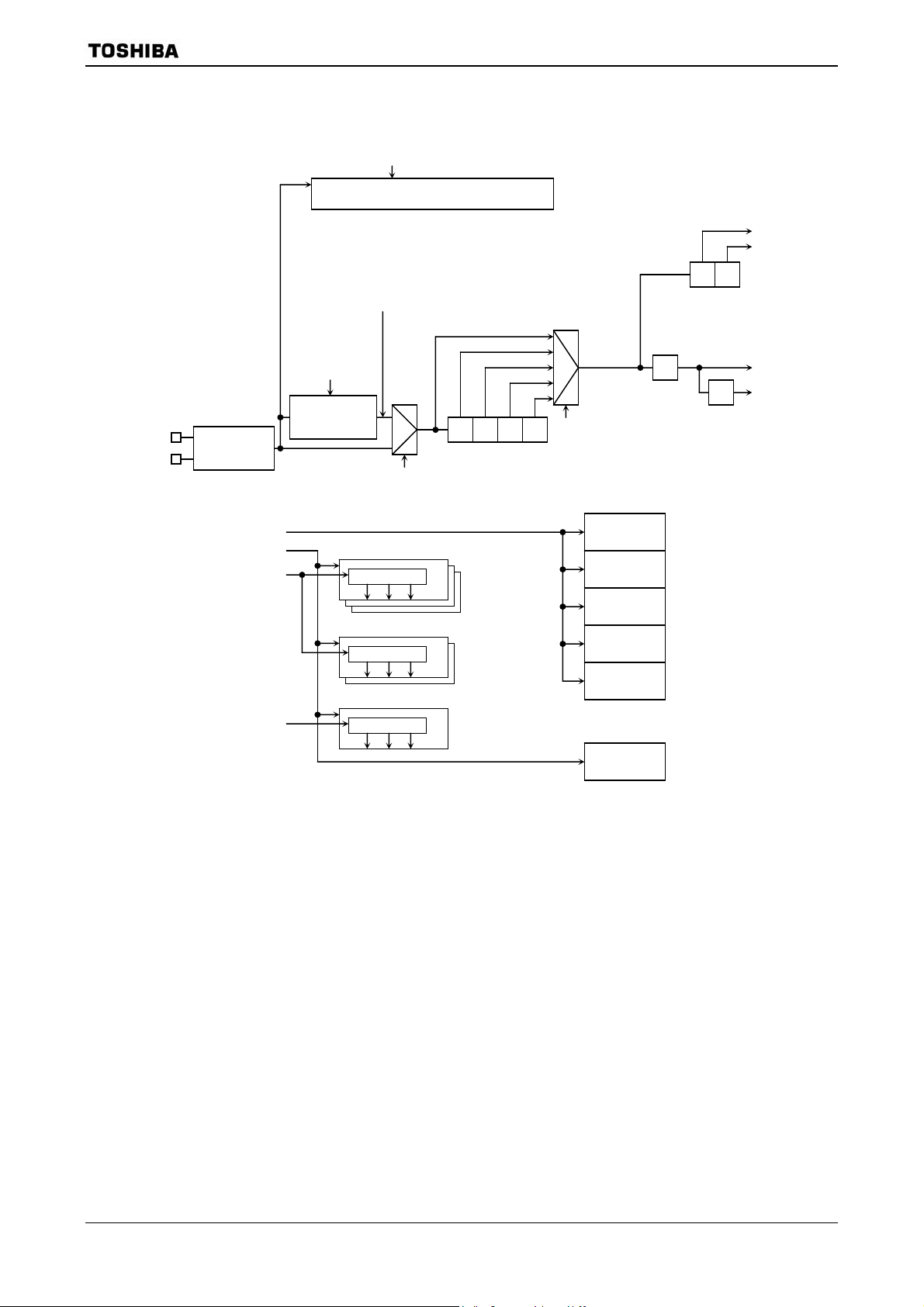
3.4.3 Interrupt Controller Operation
The block diagram in Figure 3.4.3 shows the interrupt circuits. The left-hand side of the
diagram shows the interrupt controller circuit. The right-hand side shows the CPU
interrupt request signal circuit and the halt release circuit.
For each of the 33 interrupts channels there is an interrupt request flag (Consisting of a
flip-flop), an interrupt priority setting register and a micro DMA start vector register. The
interrupt request flag latches interrupt requests from the peripherals.
The flag is cleared to 0 in the following cases:
When reset occurs
When the CPU reads the channel vector after accepted its interrupt
When executing an instruction that clears the interrupt (Write DMA start vector to
INTCLR register)
When the CPU receives a micro DMA request
When the micro DMA burst transfer is terminated
An interrupt priority can be set independently for each interrupt source by writing the
priority to the interrupt priority setting register (e.g., INTE0AD or INTE12). 6 interrupt
priorities levels (1 to 6) are provided. Setting an interrupt source’s priority level to 0 (or 7)
disables interrupt requests from that source. If interrupt request with the same level are
generated at the same time, the default priority (The interrupt with the lowest priority or,
in other words, the interrupt with the lowest vector value) is used to determine which
interrupt request is accepted first.
The 3rd and 7th bits of the interrupt priority setting register indicate the state of the
interrupt request flag and thus whether an interrupt request for a given channel has
occurred.
The interrupt controller sends the interrupt request with the highest priority among the
simultaneous interrupts and its vector address to the CPU. The CPU compares the priority
value <IFF2:0> in the status register by the interrupt request signal with the priority value
set; if the latter is higher, the interrupt is accepted. Then the CPU sets a value higher than
the priority value by 1 (+1) in the CPU SR<IFF2:0>. Interrupt request where the priority
value equals or is higher than the set value are accepted simultaneously during the
previous interrupt routine.
When interrupt processing is completed (after execution of the RETI instruction), the
CPU restores the priority value saved in the stack before the interrupt was generated to
the CPU SR<IFF2:0>.
The interrupt controller also has registers (8 channels) used to store the micro DMA start
vector. Writing the start vector of the interrupt source for the micro DMA processing (See
Table 3.4.1), enables the corresponding interrupt to be processed by micro DMA processing.
The values must be set in the micro DMA parameter register (e.g., DMAS and DMAD) prior
to the micro DMA processing.
TMP92CM22
92CM22-38
2007-02-16
Page 41

p
y
r
r
y
g
g
r
r
A
A
I
t
t
A
r
r
TMP92CM22
CPU
Interrupt controlle
Interrupt request flag
Reset
Interrupt enable
flag in CPU side
Interrupt request
signal to CPU
1
V = 20H
S Q
R
errup
n
vector read
Reset
Interrupt request
signal
DI
EI1 to 7
Interuupt
level detect
3
3
IFF2:0
INTRQ2 to 0
Priority encode
V = 24H
B
Highest
1 2 3 4 5 6 7
7
1
Y1Y2Y3Y4Y5
B
Decode
iste
re
D Q
settin
Dn
Priorit
Dn + 1
3
C
priority interrupt
6
C
CLR
Dn + 2
INTRQ2 to 0 ≥ IFF
2 to 0 then1
level select
(Highest priority
6
Y6
Interrupt
request flag
D0 D1
is “7”.)
Dn + 3
S Q
During IDLE1
D2
36
V = 28H
V = 2CH
V = 30H
Interrupt request F/F read
Interrupt vector read
Micro DMA acknowlege
R
Reset
During STOP
D3
V = 34H
V = 38H
D4
vector
Interrupt
V = 3CH
generator
V = 40H
V = 44H
D5
V = 48H
V = 4CH
D6
Release halt
D7
V = D0H
V = D4H
RESET
V = D8H
V = DCH
INT0 to INT3
NMI
Interrupt vector V
V = E0H
V = E4H
read
V = E8H
V = ECH
Micro DMA start vector setting register
Micro DMA request
If IFF = 7 then 0
4-input OR
4
Soft start
S
Selector
6
34
D Q
D5
D4
D3
Micro DMA
channel
2
2
0 1 2 3
CLR
D2
D1
D0
specification
B
encode
riorit
Micro DMA channel
DMA0V
DMA1V
DMA2V
DMA3V
INTTC0
Reset
(Reserved)
INTWD
INT0
INT1
INT2
INT3
(Reserved)
(Reserved)
(Reserved)
(Reserved)
(Reserved)
(Reserved)
INTTC0
INTTC1
INTTC2
INTTC3
INTTC4
INTTC5
INTTC6
0
Micro DMA
counte
INTTC7
interrupt
Figure 3.4.3 Block Diagram of Interrupt Controller
92CM22-39
2007-02-16
Page 42

TMP92CM22
(1) Interrupt priority setting registers
Symbol Name Address 7 6 5 4 3 2 1 0
INT2 INT1
INTE12
INTE3
INTETA01
INTETA23
INTETB0
INTETBO0
INTES0
INTES1
INTE45
INTETB1
INTETBO1
INTESB0
INTEP0
INT1&INT2
enable
INT3
enable
INTTA0&
INTTA1
enable
INTTA2&
INTTA3
enable
INTTB00&
INTTB01
enable
INTTBO0
(Overflow)
enable
INTRX0&
INTTX0
enable
INTRX1&
INTTX1
enable
INT4&
INT5
enable
INTTB10&
INTTB11
enable
INTTBO1
(Overflow)
enable
INTSBE0
enable
INTP0
enable
D0H
D1H
D4H
D5H
D8H
DAH
DBH
DCH
E0H
E1H
E2H
E3H
EEH
I2C I2M2 I2M1 I2M0 I1C I1M2 I1M1 I1M0
R R/W R R/W
0 0 0 0 0 0 0 0
− INT3
− − − − I3C I3M2 I3M1 I3M0
− − R R/W
Note: Always write “0”. 0 0 0 0
INTTA1 (TMRA1) INTTA0 (TMRA0)
ITA1C ITA1M2 ITA1M1 ITA1M0 ITA0C ITA0M2 ITA0M1 ITA0M0
R R/W R R/W
0 0 0 0 0 0 0 0
INTAT3 (TMRA3) INTAT2 (TMRA2)
ITA3C ITA3M2 ITA3M1 ITA3M0 ITA2C ITA2M2 ITA2M1 ITA2M0
R R/W R R/W
0 0 0 0 0 0 0 0
INTTB01 (TMRB0) INTTB00 (TMRB0)
ITB01C ITB01M2 ITB01M1 ITB01M0 ITB00C ITB00M2 ITB00M1 ITB00M0
R R/W R R/W
0 0 0 0 0 0 0 0
− INTTBO0 (TMRB0)
− − − − ITBO0C ITBO0M2 ITBO0M1 ITBO0M0
R R/W R R/W
Note: Always write “0”. 0 0 0 0
INTTX0 INTRX0
ITX0C ITX0M2 ITX0M1 ITX0M0 IRX0C IRX0M2 IRX0M1 IRX0M0
R R/W R R/W
0 0 0 0 0 0 0 0
INTTX1 INTRX1
ITX1C ITX1M2 ITX1M1 ITX1M0 IRX1C IRX1M2 IRX1M1 IRX1M0
R R/W R R/W
0 0 0 0 0 0 0 0
INT5 INT4
I5C I5M2 I5M1 I5M0 I4C I4M2 I4M1 I4M0
R R/W R R/W
0 0 0 0 0 0 0 0
INTTB11 (TMRB1) INTTB10 (TMRB1)
ITB11C ITB11M2 ITB11M1 ITB11M0 ITB10C ITB10M2 ITB10M1 ITB10M0
R R/W R R/W
0 0 0 0 0 0 0 0
− INTTBO1 (TMRB1)
− − − − ITBO1C ITBO1M2 ITBO1M1 ITBO1M0
− − R R/W
Note: Always write “0”. 0 0 0 0
− INTSBE0
− − − − ISBE0C ISBE0M2 ISBE0M1 ISBE0M0
− − R R/W
Note: Always write “0”. 0 0 0 0
− INTP0
− − − − IP0C IP0M2 IP0M1 IP0M0
− − R R/W
Note: Always write “0”. 0 0 0 0
92CM22-40
2007-02-16
Page 43

TMP92CM22
Symbol Name Address 7 6 5 4 3 2 1 0
INTAD INT0
INTE0AD
INTETC01
INTETC23
INTETC45
INTETC67
INTWDT
Interrupt request flag
INT0&INTAD
enable
INTTC0&
INTTC1
enable
INTTC2&
INTTC3
enable
INTTC4&
INTTC5
enable
INTTC6&
INTTC7
enable
INTWD
enable
F0H
F1H
F2H
F3H
F4H
F7H
IADC IADM2 IADM1 IADM0 I0C I0M2 I0M1 I0M0
R R/W R R/W
0 0 0 0 0 0 0 0
INTTC1 (DMA1) INTTC0 (DMA0)
ITC1C ITC1M2 ITC1M1 ITC1M0 ITC0C ITC0M2 ITC0M1 ITC0M0
R R/W R R/W
0 0 0 0 0 0 0 0
INTTC3 (DMA3) INTTC2 (DMA2)
ITC3C ITC3M2 ITC3M1 ITC3M0 ITC2C ITC2M2 ITC2M1 ITC2M0
R R/W R R/W
0 0 0 0 0 0 0 0
INTTC5 (DMA5) INTTC4 (DMA4)
ITC5C ITC5M2 ITC5M1 ITC5M0 ITC4C ITC4M2 ITC4M1 ITC4M0
R R/W R R/W
0 0 0 0 0 0 0 0
INTTC7 (DMA7) INTTC6 (DMA6)
ITC7C ITC7M2 ITC7M1 ITC7M0 ITC6C ITC6M2 ITC6M1 ITC6M0
R R/W R R/W
0 0 0 0 0 0 0 0
− INTWD
− − − − ITCWD − − −
− − R −
Note: Always write “0”. 0 − − −
IxxM2 IxxM1 IxxM0 Function (Write)
0 0 0 Disables interrupt request.
0 0 1 Sets interrupt priority level to 1.
0 1 0 Sets interrupt priority level to 2.
0 1 1 Sets interrupt priority level to 3.
1 0 0 Sets interrupt priority level to 4.
1 0 1 Sets interrupt priority level to 5.
1 1 0 Sets interrupt priority level to 6.
1 1 1 Disables interrupt request.
92CM22-41
2007-02-16
Page 44

TMP92CM22
(2) External interrupt control
Symbol Name Address 7 6 5 4 3 2 1 0
I3EDGE I2EDGE I1EDGE I0EDGE I0LE NMIREE
W R/W
0 0 0 0 0 0
INT3EDGE
0: Rising/
high
1: Falling/
low
I3LE I2LE I1LE
W
0 0 0
INT2EDGE
0: Rising/
high
1: Falling/
low
INT1EDGE
0: Rising/
high
1: Falling/
low
INT3
0: Edge
1: Level
INT0EDGE
0: Rising/
high
1: Falling/
low
INT2
0: Edge
1: Level
INT0
0: Edge
1: Level
INT1
0: Edge
1: Level
NMI
0: Falling
edge
1: Falling
and
rising
edges
IIMC
IIMC2
Interrupt
input
mode
control
Interrupt
input
mode
control2
00F6H
(Prohibit
RMW)
00FAH
(Prohibit
RMW)
Detect edge
H level
L level
Level
edge
Rising
Falling
IxLE IxEDGE
Note 1: Disable INT0 to INT3 before changing INT0 to 3 pins mode from “level” to “edge”.
Setting example for case of INT0:
DI
LD (IIMC) ,XXXXXX0-B ; Change from “level” to “edge”.
LD (INTCLR),0AH ; Clear interrupt request flag.
NOP ; Wait EI execution.
NOP
NOP
EI
X: Don’t care, −: No change
Note 2: See electrical characteristics in section 4 for external interrupt input pulse width.
Note 3: When release halt by INT0 to INT3 interrupt of level-mode in interrupt request enable, keep setting level by
<IxEDGE> until be started interrupt process. If changed “level” before interrupt process starting, interrupt
isn’t processed correctly.
Example:
Case of set “H” level interrupt (<IxLE> = 1, <IxEDGE> = 0).
Keep “H” level until be started interrupt process. If changed to “L” level before interrupt process starting,
interrupt isn’t processed correctly.
92CM22-42
2007-02-16
Page 45

Table 3.4.2 Function Setting of External Interrupt Pin
Interrupt Pin Shared Pin Mode Setting Method
Rising edge IIMC<I0LE> = 0, INT0EDGE = 0
INT0 PC3
INT1 PC1
INT2 PC5
INT3 PC6
Falling edge IIMC<I0LE> = 0, INT0EDGE = 1
High level IIMC<I0LE> = 1, INT0EDGE = 0
Low level IIMC<I0LE> = 1, INT0EDGE = 1
Rising edge IIMC2<I1LE> = 0, INT1EDGE = 0
Falling edge IIMC2<I1LE> = 0, INT1EDGE = 1
High level IIMC2<I1LE> = 1, INT1EDGE = 0
Low level IIMC2<I1LE> = 1, INT1EDGE = 1
Rising edge IIMC2<I2LE> = 0, INT2EDGE = 0
Falling edge IIMC2<I2LE> = 0, INT2EDGE = 1
High level IIMC2<I2LE> = 1, INT2EDGE = 0
Low level IIMC2<I2LE> = 1, INT2EDGE = 1
Rising edge IIMC2<I3LE> = 0, INT3EDGE = 0
Falling edge IIMC2<I3LE> = 0, INT3EDGE = 1
High level IIMC2<I3LE> = 1, INT3EDGE = 0
Low level IIMC2<I3LE> = 1, INT3EDGE = 1
INT4 PD0
INT5 PD1 Rising edge −
Rising edge TB1MOD<TB1CPM1:0> = 0, 0 or 0,1 or 1, 0
Falling edge TB1MOD<TB1CPM1:0> = 1, 0
TMP92CM22
92CM22-43
2007-02-16
Page 46

TMP92CM22
(3) SIO receive interrupt control
Symbol Name Address 7 6 5 4 3 2 1 0
IR1LE IR0LE
W
1 1
0: INTRX1
edge mode
1: INTRX1
level mode
0: INTRX0
edge mode
1: INTRX0
level mode
SIMC
SIO
Interrupt
mode
control
F5H
(Prohibit
RMW)
*INTRX1 level enables
0 Detect edge INTRX1
1 “H” leve l INTRX1
*INTRX0 rising edge enable
0 Detect edge INTRX0
1 “H” Level INTRX0
92CM22-44
2007-02-16
Page 47

TMP92CM22
(4) Interrupt request flag clear register
The interrupt request flag is cleared by writing the appropriate micro DMA start
vector, as given in
Table 3.4.1, to the register INTCLR.
For example, to clear the interrupt flag INT0, perform the following register
operation after execution of the DI instruction.
INTCLR ← 0AH Clears interrupt request flag INT0
Symbol Name Address 7 6 5 4 3 2 1 0
CLRV5 CLRV4 CLRV3 CLRV2 CLRV1 CLRV0
W
0 0 0 0 0 0
Interrupt clear
INTCLR
Interrupt
clear
control
F8H
(Prohibit
RMW)
(5) Micro DMA start vector registers
This register assigns micro DMA processing to which interrupt source. The interrupt
source with a micro DMA start vector that matches the vector set in this register is
assigned as the micro DMA start source.
When the micro DMA transfer counter value reaches “0”, the micro DMA transfer
end interrupt corresponding to the channel is sent to the interrupt controller, the micro
DMA start vector register is cleared, and the micro DMA start source for the channel is
cleared. Therefore, to continue micro DMA processing, set the micro DMA start vector
register again during the processing of the micro DMA transfer end interrupt.
If the same vector is set in the micro DMA start vector registers of more than one
channel, the channel with the lowest number has a higher priority. Accordingly, if the
same vector is set in the micro DMA start vector registers of two channels, the
interrupt generated in the channel with the lower number is executed until micro DMA
transfer is completed. If the micro DMA start vector for this channel is not set again,
the next micro DMA is started for the channel with the higher number (Micro DMA
chaining).
92CM22-45
2007-02-16
Page 48

TMP92CM22
Symbol Name Address 7 6 5 4 3 2 1 0
DMA0V5 DMA0V4 DMA0V3 DMA0V2 DMA0V1 DMA0V0
R/W
0 0 0 0 0 0
DMA0 start vector
DMA1V5 DMA1V4 DMA1V3 DMA1V2 DMA1V1 DMA1V0
R/W
0 0 0 0 0 0
DMA1 start vector
DMA2V5 DMA2V4 DMA2V3 DMA2V2 DMA2V1 DMA2V0
R/W
0 0 0 0 0 0
DMA2 start vector
DMA3V5 DMA3V4 DMA3V3 DMA3V2 DMA3V1 DMA3V0
R/W
0 0 0 0 0 0
DMA3 start vector
DMA4V5 DMA4V4 DMA4V3 DMA4V2 DMA4V1 DMA4V0
R/W
0 0 0 0 0 0
DMA4 start vector
DMA5V5 DMA5V4 DMA5V3 DMA5V2 DMA5V1 DMA5V0
R/W
0 0 0 0 0 0
DMA5 start vector
DMA6V5 DMA6V4 DMA6V3 DMA6V2 DMA6V1 DMA6V0
R/W
0 0 0 0 0 0
DMA6 start vector
DMA7V5 DMA7V4 DMA7V3 DMA7V2 DMA7V1 DMA7V0
R/W
0 0 0 0 0 0
DMA7 start vector
DMA0V
DMA1V
DMA2V
DMA3V
DMA4V
DMA5V
DMA6V
DMA7V
DMA0
start
vector
DMA1
start
vector
DMA2
start
vector
DMA3
start
vector
DMA4
start
vector
DMA5
start
vector
DMA6
start
vector
DMA7
start
vector
100H
101H
102H
103H
104H
105H
106H
107H
92CM22-46
2007-02-16
Page 49

TMP92CM22
(6) Specification of a micro DMA burst
Specifying the micro DMA burst function causes micro DMA transfer, once started,
to continue until the value in the transfer counter register reaches 0. Setting any of the
bits in the register DMAB which correspond to a micro DMA channel (as shown below)
to 1 specifies that any micro DMA transfer on that channel will be a burst transfer.
Symbol Name Address 7 6 5 4 3 2 1 0
DBST7 DBST6 DBST5 DBST4 DBST3 DBST2 DBST1 DBST0
DMAB DMA burst 108H
0 0 0 0 0 0 0 0
1: DMA request on burst mode
R/W
92CM22-47
2007-02-16
Page 50

TMP92CM22
(7) Notes
The instruction execution unit and the bus interface unit in this CPU operate
independently. Therefore if, immediately before an interrupt is generated, the CPU
fetches an instruction which clears the corresponding interrupt request flag (Note)
, the
CPU may execute this instruction in between accepting the interrupt and reading the
interrupt vector. In this case, the CPU will read the default vector 0004H and jump to
interrupt vector address FFFF04H.
To avoid this, an instruction which clears an interrupt request flag should always be
placed after a DI instruction. And in the case of setting an interrupt enable again by
EI instruction after the execution of clearing instruction, execute EI instruction after
clearing and more than 3-instructions (e.g., “NOP”× 3 times).
If placed EI instruction without waiting NOP instruction after execution of clearing
instruction, interrupt will be enable before request flag is cleared. Thus, when be
changed interrupt request level to “0”, change it after cleared corresponding interrupt
request by INTCLR instruction.
In the case of changing the value of the interrupt mask register <IFF2:0> by
execution, disable an interrupt by DI instruction before execution of POPSR
instruction.
In addition, please note that the following two circuits are exceptional and demand
special attention.
In level mode INT0 to INT3 are not an edge-triggered interrupt. Hence, in level
mode the interrupt request flip-flop for INT0 to INT3 does not function. The
peripheral interrupt request passes through the S input of the flip-flop and
becomes the Q output. If the interrupt input mode is changed from edge mode
to level mode, the interrupt request flag is cleared automatically.
If the CPU enters the interrupt response sequence as a result of INT x (x = 0, 1, 2,
or 3) going from 0 to 1, INTx must then be held at 1 until the interrupt response
sequence has been completed. If INTx is set to Level mode so as to release a
Halt state, INTx must be held at 1 from the time INTx changes from 0 to 1 until the
Halt state is released. (Hence, it is necessary to ensure that input noise is not
interpreted as a 0, causing INTx to revert to 0 before the Halt state has been
INT0 to INT3 level mode
INTRX
released.)
When the mode changes from level mode to edge mode, interrupt request flags
which were set in level mode will not be cleared. Interrupt request flags must be
cleared using the following sequence.
DI
LD (IIMC), 00H ; Changes from level to edge.
LD (INTCLR), 0AH ; Clears interrupt request flag.
NOP ; Wait EI execution.
NOP
NOP
EI
The interrupt request flip-flop can only be cleared by a reset or by reading the
serial channel receive buffer. It cannot be cleared by writing INTCLR register.
Note: The following instructions or pin input state changes are equivalent to instructions
that clear the interrupt request flag.
INT0 to INT 3: Instructions which switch to level mode after an interrupt request has
been generated in edge mode.
The pin input change from high to low after interrupt request has
been generated in level mode. (“H” → “L”, “L” →“H”)
INTRX: Instruction which read the receive buffer .
92CM22-48
2007-02-16
Page 51

3.5 Port Function
The TMP92CM22 features 50-bit settings which relate to the various I/O ports.
As well as general-purpose I/O port functionality, the port pins also have I/O functions which
relate to the built-in CPU and internal I/Os.
Table 3.5.2 and Table 3.5.3 lists I/O registers and their specifications.
TMP92CM22
Table 3.5.1 lists the functions of each port pin.
Table 3.5.1 Port Function (R: U = with pull-up resistor)
Port
Names
Port 1 P10 to P17 8 I/O − Bit D8 to D15
Port 4 P40 to P47 8 I/O* − Bit* A0 to A7
Port 5 P50 to P57 8 I/O* − Bit* A8 to A15
Port 6 P60 to P67 8 I/O* − Bit* A16 to A23
Port 7
Port 8
Port 9
Port A
Port C
Port D
Port F
Port G
Pin Names
P70 1 Output − (Fixed) RD
P71 1 Output − (Fixed) WRLL
P72 1 Output − (Fixed) WRLU
P73 1 Output − (Fixed)
P74 1 Output − (Fixed) CLKOUT
P75 1 Output − (Fixed) R/W
P76 1 I/O − Bit
P80 1 Output − (Fixed) CS0
P81 1 Output − (Fixed) CS1
P82 1 Output − (Fixed) CS2
P83 1 Output − (Fixed)
P90 1 I/O − Bit SCK
P91 1 I/O − Bit SO, SDA
P92 1 I/O − Bit SI, SCL
PA0 1 Input U (Fixed)
PA1 1 Input U (Fixed)
PA2 1 Input U (Fixed)
PA7 1 Input U (Fixed)
PC0 1 I/O − Bit TA0IN
PC1 1 I/O − Bit INT1, TA1OUT
PC3 1 I/O − Bit INT0
PC5 1 I/O − Bit INT2, TA3OUT
PC6 1 I/O − Bit INT3, TB0OUT0
PD0 1 I/O − Bit INT4, TB1IN0
PD1 1 I/O − Bit INT5, TB1IN1
PD2 1 I/O − Bit TB1OUT0
PD3 1 I/O − Bit TB1OUT1
PF0 1 I/O − Bit TXD0
PF1 1 I/O − Bit RXD0
PF2 1 I/O − Bit SCLK0, CTS0
PF3 1 I/O − Bit TXD1
PF4 1 I/O − Bit RXD1
PF5 1 I/O − Bit SCLK1, CTS1
PF6 1 I/O − Bit
PF7 1 I/O − Bit
PG0 1 Input − (Fixed) AN0
PG1 1 Input − (Fixed) AN1
PG2 1 Input − (Fixed) AN2
PG3 1 Input − (Fixed) AN3, ADTRG
PG4 1 Input − (Fixed) AN4
PG5 1 Input − (Fixed) AN5
PG6 1 Input − (Fixed) AN6
PG7 1 Input − (Fixed) AN7
Number
of Pins
Direction R
Direction
Setting Unit
Pin Names for Built-In
Function
WAIT
CS3
*: When these ports are used as general-purpose I/O port, each bit can be set individually for input or
output. However, each bit cannot be set individually for input or output even if 1bit or more bits are
used as address bus in same port.
All of general-purpose I/O ports except for port that used as address bus are operated as output
port.
Please be careful when using this setting.
92CM22-49
2007-02-16
Page 52

TMP92CM22
Table 3.5.2 I/O Port Setting List (1/2)
Ports Input Pins Specification
I/O Register Setting Value
Pn PnCR PnFC PnODE
Port 1 P10 to P17
Port 4 P40 to P47
Port 5 P50 to P57
Port 6 P60 to P67
Port 7
Port 8
Port 9
P70 to P75 Output port
P70
P71
P72
P74 CLKOUT output
P75
P76
P80 to P83 Output port × 0
P80 CS0 output × 1
P81 CS1 output × 1
P82 CS2 output × 1
P83
P90 to P92
P92
Input port
Output port
D8 to D15 bus
Input port*
Output port*
A0 to A7 output
Input port*
Output port*
A8 to A15 output
Input port*
Output port*
A16 to A23 output
RD output
WRLL output
WRLU output
R/
W output
Input port
Output port × 1 0
WAIT Input × 0
CS3 output ×
Input port
Output port × 1 0 0
SCK input × 0 0 0 P90
SCK output × × 1 0/1
SO output × 1 1 0/1 P91
SDA × × 1 1
SI input × 0 0 0
SCL (Open drain) × × 1 1
×
×
× ×
×
×
× ×
×
×
× ×
×
×
× ×
×
×
× 0
× 0 0
0
1
0*
1*
0*
1*
0*
1*
None 0
None 1
None
0
1
0
1
0
1
0
1
0
1
1
None
None
None
None
None
None
0
X: Don’t care
*: When these ports are used as gene ral-purpose I/O port, each bit can be set individually for input or
output. However, each bit cannot be set individually for input or output even if 1bit or more bit s are
used as address bus in same port.
All of general-purpose I/O ports except for port that used as address bus are operated as output
port.
Please be careful when using this setting.
92CM22-50
2007-02-16
Page 53

TMP92CM22
Table 3.5.3 I/O Port Setting List (2/2)
Ports Input Pins Specification
I/O Register Setting Value
Pn PnCR PnFC PnODE
Port A PA0, PA1,
PA2, PA7
Port C
PC3, PC5,
PC6
PC0 TA0IN input × × 1
PC3 INT0 input × × 1
PC6
Port D
PD0 TB1IN0, INT4 input × 0 1
PD1 TB1IN1, INT5 input × 0 1
PD2 TB0OUT0 output × 1 1
PD3 TB0OUT1 output × 1 1
Port F
PF1 RXD0 input × 0 None
PF4 RXD1 input × 0 None
PF5
Port G
PG3
Input port
Input port × 0 0 PC0, PC1,
Output port
TA1OUT output × 1 1 PC1
INT1 input × 0 1
INT2 input × 0 1 PC5
TA3OUT × 1 1
INT3 input × 0 1
TB0OUT0 × 1 1
Input port × 0 0 PD0 to PD3
Output port × 1 0
Input port × 0 0 PF0 to PF7
Output port × 1 0
TXD0 (Open drain) × 0 1 PF0
TXD0 × 1 1
SCLK0 input/output × 0/1 1 PF2
CTS0 input × 0 1
TXD1 (Open drain) × 0 1 PF3
TXD1 × 1 1
SCLK1 input/output × 0/1 1
CTS1 input × 0 1
Input port × PG0 to PG7
AN0 to AN7 input ×
ADTRG input ×
× None None None
× 1 0
None None None
None
None
None
X: Don’t care
By resetting, these port pins become general-purpose input port.
I/O pin is reset to input pin. When use built-in function, process all function by software.
92CM22-51
2007-02-16
Page 54

3.5.1 Port 1 (P10 to P17)
Port1 is an 8-bit general-purpose I/O port. Bits can be individually set as either
inputs or outputs by control register P1CR and function register P1FC.
In addition to functioning as a general-purpose I/O port, port1 can also function as a
data bus (D8
After released reset, device set port1 to pins of follow function by combination of AM1
and AM0 pins.
Internal data bus
to D15).
AM1 AM0 Function Setting after Reset
0 0 Don’t use this setting
0 1 Data bus (D8 to D15)
1 0 Input port (P10 to P17)
1 1 Don’t use this setting
Reset
Direction control
(on bit basis)
P1CR write
Function control
(on byte batch)
P1FC write
S
Output latch
P1 write
D8 to D15
A
Selector
B
P1 Read
External access (Data read)
Output buffer
TMP92CM22
External access (Data write)
Port 1
P10 to P17
(D8 to D15)
Figure 3.5.1 Port 1
92CM22-52
2007-02-16
Page 55

Port 1 Register
7 6 5 4 3 2 1 0
P1
(0004H)
Bit symbol P17 P16 P15 P14 P13 P12 P11 P10
Read/Write R/W
After reset Data from external port (Output latch register is clear to “0”.)
Port 1 Control Register
P1CR
(0006H)
7 6 5 4 3 2 1 0
Bit symbol P17C P16C P15C P14C P13C P12C P11C P10C
Read/Write W
After reset 0 0 0 0 0 0 0 0
Function Refer to port 1 function setting
Port 1 Function Register
7 6 5 4 3 2 1 0
P1FC
(0007H)
Bit symbol P1F
Read/Write W
After reset 0/1 Note3
Function Refer to port 1 function setting
Port 1 Function setting
Note 1: Read-modify-write instruction is prohibited for registers
P1FC and P1CR.
Note 2: <P1XC> shows “X bit” of P1CR register.
Note 3: It is set to “Port” or “Data bus” by AM pin setting.
P1CR<P1xC>
P1FC<P1F>
0 1
0 Input port
1 Output port
TMP92CM22
Data bus
(D15 to D8)
Don’t use this
setting
Figure 3.5.2 Register for Port 1
92CM22-53
2007-02-16
Page 56

A
3.5.2 Port 4 (P40 to P47)
Port 4 is an 8-bit general-purpose I/O port*. Bits can be individually set as either inputs
or outputs by control register P4CR and function register P4FC*.
In addition to functioning as a general-purpose I/O port, port 4 can also function as a
address bus (A0 to A7).
After released reset, device set Port 4 to pins of follow function by combination of AM1
and AM0 pins.
*: When these ports are used as general-purpose I/O port, each bit can be set individually for input or output. However, each
bit cannot be set individually for input or output even if 1bit or more bits are used as address bus in same port.
All of general-purpose I/O ports except for port that used as address bus are operated as output port.
Please be careful when using this setting.
Reset
Internal data bus
AM1 AM0 Function Setting after Reset
0 0 Don’t use this setting
0 1 Address bus (A0 to A7)
1 0 Address bus (A0 to A7)
1 1 Don’t use this setting
Internal address bus
B
Selector
A
0 to A7
S
Output buffer
Direction control
(on bit basis)*
P4CR write
Function control
(on bit basis)
P4FC write
Output latch
P4 write
P4 read
TMP92CM22
Port 4
P40 to P47
(A0 to A7)
Figure 3.5.3 Port 4
92CM22-54
2007-02-16
Page 57

P4
(0010H)
P4CR
(0012H)
P4FC
(0013H)
TMP92CM22
Port 4 Register
7 6 5 4 3 2 1 0
Bit symbol P47 P46 P45 P44 P43 P42 P41 P40
Read/Write R/W
After reset Data from external port (Output latch register is cleared to “0”.)
Port 4 Control Register
7 6 5 4 3 2 1 0
Bit symbol P47C P46C P45C P44C P43C P42C P41C P40C
Read/Write W
After reset 0 0 0 0 0 0 0 0
Function 0: Input 1: Output (Note2)
Port 4 Function Register
7 6 5 4 3 2 1 0
Bit symbol P47F P46F P45F P44F P43F P42F P41F P40F
Read/Write W
After reset 1 1 1 1 1 1 1 1
Function 0: Port 1: Address bus (A0 to A7)
Note1: Read-modify-write instruction is prohibited for registers P4CR and P4FC.
Note2: When these ports are used as general-purpose I/O port, each bit can be set individually for input or output.
However, each bit cannot be set individually for input or output even if 1bit or more bits are used as address
bus in same port. All of general-purpose I/O ports except for port that used as address bus are opera ted as
output port. Please be careful when using this setting.
Figure 3.5.4 Register for Port 4
92CM22-55
2007-02-16
Page 58

A
3.5.3 Port 5 (P50 to P57)
Port 5 is an 8-bit general-purpose I/O port*. Bits can be individually set as either inputs
or outputs by control register P5CR and function register P5FC*.
In addition to functioning as a general-purpose I/O port, port 5 can also function as an
address bus (A8 to A15).
After released reset, device set port 5 to pins of follow function by combination of AM1
and AM0 pins.
*: When these ports are used as general-purpose I/O port, each bit can be set individually for input or output. However, each
bit cannot be set individually for input or output even if 1bit or more bits are used as address bus in same port.
All of general-purpose I/O ports except for port that used as address bus are operated as output port.
Please be careful when using this setting.
Reset
Internal data bus
AM1 AM0 Function Setting after Reset
0 0 Don’t use this setting
0 1 Address bus (A8 to A15)
1 0 Address bus (A8 to A15)
1 1 Don’t use this setting
Internal address bus
8 to A15
Direction control
(on bit basis)*
P5CR write
Function control
(on bit basis)
S
B
P5FC write
Output latch
P5 write
A
P5 read
Selector
Output buffer
TMP92CM22
Port 5
P50 to P57
(A8 to A15)
Figure 3.5.5 Port 5
92CM22-56
2007-02-16
Page 59

P5
(0014H)
P5CR
(0016H)
P5FC
(0017H)
TMP92CM22
Port 5 Register
7 6 5 4 3 2 1 0
Bit symbol P57 P56 P55 P54 P53 P52 P51 P50
Read/Write R/W
After reset Data from external port (Output latch register is cleared to “0”.)
Port 5 Control Register
7 6 5 4 3 2 1 0
Bit symbol P57C P56C P55C P54C P53C P52C P51C P50C
Read/Write W
After reset 0 0 0 0 0 0 0 0
Function 0: Input 1: Output (Note2)
Port 5 Function Register
7 6 5 4 3 2 1 0
Bit symbol P57F P56F P55F P54F P53F P52F P51F P50F
Read/Write W
After reset 1 1 1 1 1 1 1 1
Function 0: Port 1: Address bus (A8 to A15)
Note1: Read-modify-write instruction is prohibited for registers P5CR and P5FC.
Note2: When these ports are used as general-purpose I/O port, each bit can be set individually for input or output.
However, each bit cannot be set individually for input or output even if 1bit or more bits are used as address
bus in same port. All of general-purpose I/O ports except for port that used as address bus are opera ted as
output port. Please be careful when using this setting.
Figure 3.5.6 Register for Port 5
92CM22-57
2007-02-16
Page 60

A
3.5.4 Port 6 (P60 to P67)
Port 6 is an 8-bit general-purpose I/O port*. Bits can be individually set as either inputs
or outputs by control register P6CR and function register P6FC*.
In addition to functioning as a general-purpose I/O port, port 6 can also function as an
address bus (A16 to A23).
After released reset, device set port 6 to pins of follow function by combination of AM1
and AM0 pins.
*: When these ports are used as general-purpose I/O port, each bit can be set individually for input or output. However, each
bit cannot be set individually for input or output even if 1bit or more bits are used as address bus in same port.
All of general-purpose I/O ports except for port that used as address bus are operated as output port.
Please be careful when using this setting.
Reset
Internal data bus
AM1 AM0 Function Setting after Reset
0 0 Don’t use this setting
0 1 Address bus (A16 to A23)
1 0 Address bus (A16 to A23)
1 1 Don’t use this setting
Internal address bus
16 to A23
Direction control
(on bit basis)*
P6CR write
Function control
(on bit basis)
S
B
P6FC write
Output latch
P6 write
A
P6 read
Selector
Output buffer
TMP92CM22
Port 6
P60 to P67
(A16 to A23)
Figure 3.5.7 Port 6
92CM22-58
2007-02-16
Page 61

P6
(0018H)
P6CR
(001AH)
P6FC
(001BH)
TMP92CM22
Port 6 Register
7 6 5 4 3 2 1 0
Bit symbol P67 P66 P65 P64 P63 P62 P61 P60
Read/Write R/W
After reset Data from external port (Output latch register is cleared to “0”.)
Port 6 Control Register
7 6 5 4 3 2 1 0
Bit symbol P67C P66C P65C P64C P63C P62C P61C P60C
Read/Write W
After reset 0 0 0 0 0 0 0 0
Function 0: Input 1: Output (Note2)
Port 6 Function Register
7 6 5 4 3 2 1 0
Bit symbol P67F P66F P65F P64F P63F P62F P61F P60F
Read/Write W
After reset 1 1 1 1 1 1 1 1
Function 0: Port 1: Address bus (A16 to A23)
Note1: Read-modify-write instruction is prohibited for registers P6CR and P6FC.
Note2: When these ports are used as general-purpose I/O port, each bit can be set individually for input or output.
However, each bit cannot be set individually for input or output even if 1bit or more bits are used as address
bus in same port. All of general-purpose I/O ports except for port that used as address bus are opera ted as
output port. Please be careful when using this setting.
Figure 3.5.8 Register for Port 6
92CM22-59
2007-02-16
Page 62

3.5.5 Port 7 (P70 to P76)
Port 7 is a 7-bit general-purpose I/O port (P70 to P75 are used for output only).
Bits can be individually set as either inputs or outputs by control register P7CR and
function register P7FC.
In addition to functioning as a general-purpose I/O port, P70 to P73 pins can also
function as output pin of read/write strobe signals to connect with an external memory. P74
pin can also function as CLKOUT output pin when outputted internal clock. P76 pin can
also function as wait input.
After reset, P71 to P75 pins are set to output port mode, and P76 pin is set to input port
mode.
P70 pin set port 1 to pins of follow function by combination of AM1 and AM0 pins.
Reset
Internal data bus
AM1 AM0 Function Setting after Reset
0 0 Don’t use this setting
0 1 CPU control pin (RD)
1 0 CPU control pin (RD )
1 1 Don’t use this setting
Function control
(on bit basis)
P7FC write
S
Output latch
P7 write
P7 read
RD , WRLL ,
CLKOUT, R/
Note: P73 is fixed to VCC.
A
Selector
B
WRLU
W
Output buffer
,
Port 7
RD )
P70 (
WRLL )
P71 (
WRLU )
P72 (
P73
P74 (CLKOUT)
W )
P75 (R/
TMP92CM22
Figure 3.5.9 Port 7 (P70 to P75)
92CM22-60
2007-02-16
Page 63

TMP92CM22
Reset
Direction control
(on bit basis)
P7CR write
Function control
(on bit basis)
Internal data bus
P7FC write
S
Output latch
Output buffer
Port P7
P76 (
WAIT
)
P7 write
P7 read
Internal WAIT signal
P7
(001CH)
P7CR
(001EH)
P7FC
(001FH)
Figure 3.5.10 Port 7 (P76)
Port 7 Register
7 6 5 4 3 2 1 0
Bit symbol P76 P75 P74 P73 P72 P71 P70
Read/Write R/W
After reset Data from
external
port (Note)
Note: Output latch register is cleared to 0.
1 1 1 1 1 1
Port 7 Control Register
7 6 5 4 3 2 1 0
Bit symbol P76C
Read/Write W
After reset 0
Function
0: Input
1: Output
Port 7 Function Register
7 6 5 4 3 2 1 0
Bit symbol P76F P75F P74F P73F P72F P71F P70F
Read/Write W
After reset 0 0 0 0 0 0 1
Function 0: Port
WAIT
1:
Note: Read-modify-write instruction is prohibited for registers P7CR and P7FC.
0: Port
1: R/ W
0: Port
1: CLKOUT
0: Port
Don’t set
1:
0: Port
WRLU
1:
0: Port
WRLL
1:
0: Port
1: RD
Figure 3.5.11 Register for Port 7
92CM22-61
2007-02-16
Page 64

3.5.6 Port 8 (P80 to P83)
Port 8 is 4-bit output port. Resetting sets output latch of P82 to “0” and set output
latches of P80, P81, and P83 to “1”.
In addition to functioning as a output port, port 8 can also function as a output chip select
signal (
CS0 to CS3 ).
These settings operate by programming “1” to the corresponding bit of P8FC.
Resetting set all bits of P8FC to “0”, these pits set output mode.
Reset
Internal data bus
Function control
(on bit basis)
P8FC write
Output latch
P8 write
A
Selector
B
TMP92CM22
S
P80 ( CS0 )
CS1 )
P81 (
P82 (
P83 (
CS2 )
CS3 )
P8
(0020H)
P8FC
(0023H)
P8 read
CS0 , CS1 , CS2, CS3
Figure 3.5.12 Port 8
Port 8 Register
7 6 5 4 3 2 1 0
Bit symbol P83 P82 P81 P80
Read/Write R/W
After reset 1 0 1 1
Port 8 Function Register
7 6 5 4 3 2 1 0
Bit symbol P83F P82F P81F P80F
Read/Write W
After reset 0 0 0 0
Function
Note 1: Read-modify-write instruction is prohibited for the registers P8FC.
Note 2: When set P82 pin as
P82 to “0” (P8<P82> = 0).
If set function register (P8FC<P82F> = 1) after set output latch to “1” (P8<P82> = 1), maybe operation become
to error because
after release reset, set function register (P8FC<P82F> = 1) in keep output latch of
2CS
output don’t output correctly.
2CS
0: Port
1:
0: Port
1:
3CS
0: Port
1:
2CS
0: Port
1:
1CS
0CS
Figure 3.5.13 Register for Port 8
92CM22-62
2007-02-16
Page 65

3.5.7 Port 9 (P90 to P92)
Port 9 is 3-bit general-purpose I/O port. Each bit can be set individually for input or
output.
In addition to functioning as a general-purpose I/O port, port 9 can also function as a
serial bus interface input (SCK (Clock signal in SIO mode), SO (Data output signal in SIO
mode), SDA (Data signal in I
(Clock signal in I
These settings operate by programming to the corresponding bit of P9FC.
Resetting set value of P9CR and P9FC to “0”, all bits are set to input port. And all bits of
output latch are set to “1”.
Reset
Internal data bus
SCK input
SDA input
SI/SCL input
2
C bus mode)).
Direction control
(on bit basis)
P9CR write
Function control
(on bit basis)
P9FC write
S
Output latch
P9 write
SCK output
SO output
SDA output
SCL output
P9 read
TMP92CM22
2
C bus mode), SI (Data input signal in SIO mode) and SCL
S
A
Selector
B
S
Selector
Open-drain enable
P9ODE<P91ODE>
<P92ODE>
B
A
P90 (SCK),
P91 (SO/SDA)
P92 (SI/SCL)
Figure 3.5.14 Port 9 (P90 to P92)
92CM22-63
2007-02-16
Page 66

P9
(0024H)
P9CR
P9CR
(0026H)
(0026H)
P9FC
P9FC
(0027H)
(0027H)
P9ODE
(0025H)
TMP92CM22
Port 9 Register
7 6 5 4 3 2 1 0
Bit symbol P92 P91 P90
Read/Write R/W
After reset Data from external port
(Output latch register is set to 1)
Port 9 Control Register
7 6 5 4 3 2 1 0
Bit symbol P92C P91C P90C
Read/Write W
After reset 0 0 0
Function 0: Input 1: Output
Port 9 Function Register
7 6 5 4 3 2 1 0
Bit symbol P92F P91F P90F
Read/Write W
After reset 0 0 0
Function 0: Port, SI
1: SCL
Note
0: Port
1: SO,
SDA
0: Port,
SCK input
1:SCK output
Note
Port 9 ODE Register
7 6 5 4 3 2 1 0
Bit symbol P92ODE P91ODE
Read/Write W
After reset 0 0
Function 1:Open drain 1:Open drain
Note1: Read-modify-write instruction is prohibited for the registers P9CR, P9FC, and P9ODE.
Note2: When using SI and SCK input function, set P9FC<P92F,P90F> to “0” (Function setting).
Figure 3.5.15 Register for Port 9
92CM22-64
2007-02-16
Page 67

3.5.8 Port A (PA0 to PA2, PA7)
Port A is 4-bit general-purpose input port with pull-up resistor.
Internal data bus
7 6 5 4 3 2 1 0
PA
(0028H)
Bit symbol PA7 PA2 PA1 PA0
Read/Write R R
After reset Data from
external port
TMP92CM22
Pull-up resistor
PA0, PA1,
PA2, PA7
PA read
Figure 3.5.16 Port A
Port A Register
Data from external port
Figure 3.5.17 Register for Port A
92CM22-65
2007-02-16
Page 68

3.5.9 Port C (PC0, PC1, PC3, PC5, and PC6)
Port C is 5-bit general-purpose I/O port. Each bit can be set individually for input or
output. Resetting sets port C to input port.
In addition to functioning as a general-purpose I/O port, port C can also function as a
input/output pin (TA0IN, TA1OUT, TA3OUT, and TB0OUT0) and external interrupt pin
(INT0 to INT3).
These settings operate by programming “1” to the corresponding bit of PCCR and PCFC.
Resetting resets the PCCR and PCFC to “0”, and sets all bits to input port.
(1) PC0 (TA0IN)
In addition to function as I/O port, port PC0 can also function as input pin TA0IN of
timer channel 0.
Reset
Direction control
(on bit basis)
TMP92CM22
PCCR write
Function control
(on bit basis)
Internal data bus
TA0IN
PCFC write
S
Output latch
PC write
PC read
S
Selector
PC0 (TA0IN)
B
A
Note: Can not read the output latch data when output mode.
Figure 3.5.18 Port C (PC0)
92CM22-66
2007-02-16
Page 69

TMP92CM22
(2) PC1 (INT1, TA1OUT), PC5 (INT2, TA3OUT), PC6 (INT3, TB0OUT0)
In addition to function as I/O port, port PC1, PC5, and PC6 can also function as
external interrupt input pin INT1 to INT3 and output pin of timer channel TA1OUT,
TA3OUT, and TB0OUT0.
Reset
Direction control
(on bit basis)
PCCR write
Function control
(on bit basis)
Internal data bus
INT1
INT2
INT3
PCFC write
S
Output latch
PC write
TA1OUT
TA3OUT
TB0OUT0
PC read
Selector
S B
IIMC2<I1LE, I2LE, I3LE>
A
Selector
B
A
S
PC1 (INT1, TA1OUT)
PC5 (INT2, TA3OUT)
PC6 (INT3, TB0OUT0)
S
B
Selector
A
Select rising/falling
IIMC <I1EDGE, I2EDGE, I3EDGE>
High level/low level selection
Note: Can not read the output latch data when output mode.
Figure 3.5.19 Port C (PC1, PC5, and PC6)
92CM22-67
2007-02-16
Page 70

TMP92CM22
(3) PC3 (INT0)
In addition to function as I/O port, port PC3 can also function as external interrupt
pin INT0.
Reset
Direction control
(on bit basis)
PCCR write
Function control
(on bit basis)
PCFC write
Internal data bus
S
Output latch
PC3 (INT0)
PC read
S
B
Selector
PC read
INT0
A
Select level/edge
and
Select rising/falling
IIMC<I0LE, I0EDGE>
Figure 3.5.20 Port C (PC3)
92CM22-68
2007-02-16
Page 71

PC
(0030H)
PCCR
PCCR
(0032H)
(0032H)
PCFC
PCFC
(0033H)
(0033H)
TMP92CM22
Port C Register
7 6 5 4 3 2 1 0
Bit symbol PC6 PC5 PC3 PC1 PC0
Read/Write R/W R/W R/W
After reset Data from external
port (Note)
Note: Output latch register is set to 1.
Data from
external
port (Note)
Data from external
port (Note)
Port C Control Register
7 6 5 4 3 2 1 0
Bit symbol PC6C PC5C PC3C PC1C PC0C
Read/Write W W W
After reset 0 0 0 0 0
Function 0: Input 1: Output 0: Input
1: Output
0: Input 1: Output
Port C Function Register
7 6 5 4 3 2 1 0
Bit symbol PC6F PC5F PC3F PC1F PC0F
Read/Write W W W
After reset 0 0 1 0 0
Function 0: Port
1: INT3
TB0OUT0
Note 1: Read-modify-write instruction is prohibited for the registers PCCR and PCFC.
Note 2: PC0/TA0IN pins do not have a register changing PORT/FUNCTION. For example, when it is used as an input
port, the input signal is inputted to 8-bit timer as the input 0.
Note 3: Can not read the output latch data when PC0, PC1, PC5, and PC6 are output mode.
0: Port
1: INT2
TA3OUT
0: Port
1: INT0
0: Port
1: INT1
TA1OUT
INT1, TA1OUT setting
<PC1C>
<PC1F>
0 Input port Output port
1 INT1 TA1OUT
<PC5C>
<PC5F>
0 Input port Output port
1 INT2 TA3OUT
<PC6C>
<PC6F>
0 Input port Output port
1 INT3 TB0OUT0
0 1
INT2, TA3OUT Setting
0 1
INT3, TB0OUT0 setting
0 1
0: Port
1: TA0IN
Figure 3.5.21 Register for Port C
92CM22-69
2007-02-16
Page 72

3.5.10 Port D (PD0 to PD3)
Port D is 4-bit general-purpose I/O port. Each bit can be set individually for input or
output. Resetting sets port D to input port.
In addition to functioning as a general-purpose I/O port, port D can also function as an
input pin (INT4 and INT5)/output pin (TB0IN, TB1OUT, TB3OUT, and TB1OUT1).
These settings operate by programming “1” to the corresponding bit of PDCR and PDFC.
Resetting resets the PDCR and PDFC to “0”, and sets all bits to input port.
(1) PD0 (INT4, TB1IN0), PD1 (INT5, TB1IN1)
In addition to function as I/O port, port PD0 and PD1 can also function as external
interrupt input pins INT4, INT5, timer channel input pins TB1IN0 and TB1IN1.
Reset
TMP92CM22
Direction control
(on bit basis)
PDCR write
Function control
(on bit basis)
PDFC write
Internal address bus
INT4, TB1IN0
INT5, TB1IN1
S
Output latch
PD write
PD read
PD0 (INT4, TB1IN0)
PD1 (INT5, TB1IN1)
S
B
Selector
A
Note: Can not read the output latch data when output mode.
Figure 3.5.22 Port D (PD0 and PD1)
92CM22-70
2007-02-16
Page 73

(
)
TMP92CM22
(2) PD2 (TB1OUT0) and PD3 (TB1OUT1)
In addition to function as I/O port, port PD0 and PD1 can also function as timer
channel output pins TB1OUT0 and TB1OUT1.
Reset
Direction control
(on bit basis)
PDCR write
Function control
(on bit basis)
Internal data bus
PDFC write
Output latch
PD write
TB1OUT0
TB1OUT1
S
PF read
S
A
Selector
B
S
Selector
PD2 (TB1OUT0)
TB1OUT1
PD3
B
A
Figure 3.5.23 Port D (PD2 and PD3)
92CM22-71
2007-02-16
Page 74

PD
(0034H)
PDCR
(0036H)
TMP92CM22
Port D Register
7 6 5 4 3 2 1 0
Bit symbol PD3 PD2 PD1 PD0
Read/Write R/W
After reset Data from external port
(Output latch register is set to 1)
Port D Control Register
7 6 5 4 3 2 1 0
Bit symbol PD3C PD2C PD1C PD0C
Read/Write W
After reset 0 0 0 0
Function 0: Input
1: Output
0: Input
1: Output
0: Input
1: Output
Port D I/O setting
0: Input
1: Output
0 Input
1 Output
PDFC
(0037H)
Port D Function Register
7 6 5 4 3 2 1 0
Bit symbol PD3F PD2F PD1F PD0F
Read/Write W
After reset 0 0 0 0
Function 0: Port
1: TB1OUT1
Note 1: Read-modify-write instruction is prohibited for the registers PDFC and PDCR.
Note 2: Can not read the output latch data when PD0 and PD1 are output mode.
0: Port
1: TB1OUT0
0: Port
1: TB0IN1
INT5 Input
PD2 output setting asTB1OUT0
PD3 output setting as TB1OUT1
0: Port
1: TB0IN0
INT4 Input
PDFC<PD2F> 1
PDCR<PD2C> 1
PDFC<PD3F> 1
PDCR<PD3C> 1
Figure 3.5.24 Register for Port D
92CM22-72
2007-02-16
Page 75

(
)
3.5.11 Port F (PF0 to PF7)
Port F is 8-bit general-purpose I/O port. Each bit can be set individually for input or
output. Resetting resets the PFCR and PFFC to “0”, and sets all bits to input port. And all
bits of output latch register to “1”.
In addition to functioning as a general-purpose I/O port, port F can also function as I/O
function of serial channel 0 and 1.
These settings operate by writing “1” to the corresponding bit of PFFC.
Resetting resets the PDCR and PDFC to “0”, and sets all bits to input port.
(1) Port PF0 and PF3 (TXD0/TXD1)
In addition to function as I/O port, port PF0 and PF3 can also function as TXD output
pin of serial channel.
Thus, output buffer feature a programmable open-drain function, and setting enable by
PFFC<PF0F, PF3F> and PFCR<PF0C, PF3C> register.
Direction control
TMP92CM22
Reset
(on bit basis)
PFCR write
Function control
(on bit basis)
PFFC write
Internal data bus
S
Output latch
TXD0, TXD1
PF write
PF read
S
A
Selector
B
S
Selector
Open-drain enable
<PF0F = 1, PF0C = 0
PF3F = 1, PF3C = 0>
B
A
PF0 (TXD0)
TXD1
PF3
Figure 3.5.25 Port F (PF0 and PF3)
92CM22-73
2007-02-16
Page 76

TMP92CM22
(2) Ports PF1 and PF4 (RXD0 and XD1)
In addition to function as I/O port, port PF1 and PF4 can also function as RXD input
pin of serial channel.
Reset
Direction control
(on bit basis)
PFCR write
Internal data bus
S
Output latch
PF write
PF read
S
Selector
PF1 (RXD0)
PF4 (RXD1)
B
A
RXD0, RXD1
Figure 3.5.26 Port F (PF and PF4)
92CM22-74
2007-02-16
Page 77

p
TMP92CM22
(3) Port PF2 (
In addition to function as I/O port, port PF2 and PF5 can also function as
, SCLK0) and port PF5 (
CTS0
CTS1
, SCLK1)
CTS input
pin of serial channel or SCLK I/O pin.
Reset
Direction control
(on bit basis)
PFCR write
Function control
(on bit basis)
Internal data bus
PFFC write
S
Output latch
SCLK0, SCLK1
PF write
PF read
CTS0 , CTS1
SCLK0, SCLK1
input
out
S
A
Selector
B
ut
S
B
Selector
A
PF2 (SCLK0, CTS0 )
PF5 (SCLK1,
CTS1)
Figure 3.5.27 Port F (PF2 and PF5)
(4) Port PF6 and port PF7
These ports are general-purpose I/O port.
Reset
R
Direction control
(on bit basis)
PFCR write
S
Internal data bus
Output latch
PF write
PF read
S
Selector
B
A
PF6 to PF7
Figure 3.5.28 Port F (PF6 and PF7)
92CM22-75
2007-02-16
Page 78

PF
(003CH)
PFCR
PFCR
(003EH)
(003EH)
PFFC
PFFC
(003FH)
(003FH)
TMP92CM22
Port F Register
7 6 5 4 3 2 1 0
Bit symbol PF7 PF6 PF5 PF4 PF PF2 PF1 PF0
Read/Write R/W
After reset Data from external port (Output latch register is set to 1)
Port F Control Register
7 6 5 4 3 2 1 0
Bit symbol PF7C PF6C PF5C PF4C PF3C PF2C PF1C PF0C
Read/Write W
After reset 0 0 0 0 0 0 0 0
Function 0: Input 1: Output
Port F Function Register
7 6 5 4 3 2 1 0
Bit symbol − − PF5F PF3F PF2F PF0F
Read/Write W W W
After reset 0 0 0 0 0 0
Function Always
write “0”.
Port function setting
<PF3C>
<PF3F>
0 Input port Output port
1
<PF0C>
<PF0F>
0 Input port Output port
1
Note 1: Read-modify-write instruction is prohibited for the registers PFCR and PFFC.
Note 2: PF1/RXD0 and PF4/RXD1 pins do not have a regi ster changing PORT/ FUN CTI O N. For e xample, when it is
Note 3: PF0 and PF3 pi ns do not have a register (PFODE) for open-drain setting. Please conduct the open-drain
0 1
TXD1
(Open drain)
0 1
TXD0
(Open drain)
used as an input port, the input signal is inputted to SIO as the serial receive data.
setting according to above setting.
Always
write “0”.
TXD1
TXD0
0: Port
1: SCLK1
output
0: Port
1: TXD1
0: Port
1: SCLK0
output
0: Port
1: TXD0
Figure 3.5.29 Register for Port F
92CM22-76
2007-02-16
Page 79

3.5.12 Port G (PG0 to PG7)
Port G is 8-bit input port and can also be used as the analog input pins for the internal
AD converter. PG3 can also be used as ADTRG pin for the AD converter.
PG read
TMP92CM22
Port G
PG0 to PG7
(AN0 to AN7)
PG
(0040H)
Convertion
result
Internal data bus
AD read
ADTRG
(only PG3)
register
AD
converter
Channel
selector
Figure 3.5.30 Port G
Port G Register
7 6 5 4 3 2 1 0
Bit symbol PG7 PG6 PG5 PG4 PG3 PG2 PG1 PG0
Read/Write R
After reset Data from external port
Note: The input channel selection of AD converter and the permission of ADTRG input are set by AD converter mode
register ADMOD1.
Figure 3.5.31 Register for Port G
92CM22-77
2007-02-16
Page 80

3.6 Memory Controller
3.6.1 Function
TMP92CM22 has a memory controller with a variable 4-block address area that controls
as follows.
(1) 4-block address area support
Specifies a start address and a block size for 4-block address area.
(2) Connecting memory specifications
Specifies SRAM and ROM as memories to connect with the selected address areas.
(3) Data bus size selection
Whether 8-bit or 16-bit is selected as the data bus size of the respective block address
areas.
(4) Wait control
Wait specification bit in the control register and WAIT input pin control the number of
waits in the external bus cycle. Read cycle and write cycle can specify the number of
waits individually.
The number of waits is controlled in 6 mode mentioned below.
TMP92CM22
0 waits, 1 wait,
2 waits, 3 waits, 4 waits
N waits (Control with WAIT pin)
92CM22-78
2007-02-16
Page 81

3.6.2 Control Register and Operation after Reset Release
This section describes the registers to control the memory controller, the state after reset
release and necessary settings.
(1) Control register
The control registers of the memory controller are as follows.
• Control register: BnCSH/BnCSL (n = 0 to 3, EX)
Sets the basic functions of the memory controller, that is the connecting
memory type, the number of waits to be read and written.
• Memory start address register: MSARn (n = 0 to 3)
Sets a start address in the selected block address areas.
• Memory address mask register: MAMRn (n = 0 to 3)
Sets a block size in the selected address areas.
In addition to setting of the above-mentioned registers, it is necessary to set the
following registers to control ROM page mode access.
• Page ROM control register: PMEMCR
Sets to executed ROM page mode accessing.
TMP92CM22
(2) Operation after reset release
The start data bus width is determined depending on state of AM1 and AM0 pins
just after reset release. Then, the external memory is accessed as follows.
AM1 AM0 Start Mode
0 0 Don’t use this setting
0 1 Start with 16-bit data bus
1 0 Start with 8-bit data bus
1 1 Don’t use this setting
AM1/AM0 pins are valid only just after reset release. In the other cases, the
data bus width is set to the value set to BnBUS bit of the control register.
By reset, only control register (B2CSH/B2CSL) of the block address area 2 is
automatically effective (B2CSH<B2E> is set to “1” by reset).
The data bus width which is specified by AM1/AM0 pin is loaded to the bit to
specify the bus width of the control register in the block address area 2.
The block address area 2 is set to address 000000H to FFFFFFH by reset.
After reset release, the block address areas are specified by the memory start
address register (MSAR) and the memory address mask register (MAMR). Then
the control register (BnCS) is set.
Set the enable bit (BnE) of the control register to “1” to enable the setting.
92CM22-79
2007-02-16
Page 82

3.6.3 Basic Functions and Register Setting
In this section, setting of the block address area, the connecting memory and the
number of waits out of the memory controller’s functions are described.
(1) Block address area specification
The block address area is specified by two registers.
The memory start address register (MSAR) sets the start address of the block
address areas. The memory controller compares between the register value and the
address every bus cycles. The address bit which is masked by the memory address
mask register (MAMR) is not compared by the memory controller. The block address
area size is determined by setting the memory address mask register. The set value in
the register is compared with the block address area on the bus. If the compared result
is a match, the memory controller sets the chip select signal (
(i) Setting memory start address register
The MS23 to MS16 bits of the memory start address register respectively
correspond with addresses A23 to A16. The lower start address A15 to A0 are
always set to address 0000H.
TMP92CM22
CS ) to “low”.
Therefore the start address of the block address area are set to addresses
000000H to FF0000H every 64 Kbytes.
(ii) Setting memory address mask registers
The memory address mask register sets whether an address bit is compared or
not. Set the register to “0” to compare, or to “1” not to compare.
The address bit to be set is depended on the block address area.
Block address area 0: A20 to A8
Block address area 1: A21 to A8
Block address area 2 to 3: A22 to A15
The above-mentioned bits are always compared. The block address area size is
determined by the compared result.
The size to be set depending on the block address area is as follows.
Size (bytes)
CS area
CS0 ○ ○ ○ ○ ○ ○ ○ ○ ○
CS1 ○ ○ ○ ○ ○ ○ ○ ○ ○
CS2 to CS3 ○ ○ ○ ○ ○ ○ ○ ○ ○
256 512 32 K 64 K 128 K 256 K 512 K 1 M 2 M 4 M 8 M
Note: After reset release, only the control register of the block address area 2 is valid. The control
register of the block address area 2 has <B2M> bit. Setting <B2M> bit to “0” sets the block
address area 2 to addresses 000000H to FFFFFFH. State of after reset release is set this.
Setting <B2M> bit to “1” specifies the start address and the address area size as it is in the other
block address area.
92CM22-80
2007-02-16
Page 83

TMP92CM22
(iii) Example of register setting
To set the block address area 1 to 512 bytes from address 110000H, set the
register as follows.
MSAR1 Register
7 6 5 4 3 2 1 0
Bit symbol M1S23 M1S22 M1S21 M1S20 M1S19 M1S18 M1S17 M1S16
Setting value 0 0 0 1 0 0 0 1
M1S23 to M1S16 bits of the memory start address register MSAR1 correspond
with address A23 to A16.
A15 to A0 are cleared to “0”. Therefore setting MSAR1 to the above-mentioned
value specifies the start address of the block address area to address 110000H.
The start address is set as it is in the other block address areas.
MAMR1 Register
7 6 5 4 3 2 1 0
Bit symbol M1V21 M1V20 M1V19 M1V18 M1V17 M1V16 M1V15-9 M1V8
Setting value 0 0 0 0 0 0 0 1
M1V21 to M1V16 and M1V8 bits of the memory address mask register
MAMR1 set whether address A21 to A16 and A8 are compared or not. Set the
register to “0” to compare, or to “1” not to compare. A23 and A22 are always
compared.
Setting the above-mentioned compares A23 to A9 with the values set as the
start addresses. Therefore 512 bytes of addresses 110000H to 1101FFH are set
as the block address area 1, and compared with the addresses on the bus. If the
compared result is a match, the chip select signal
CS1 is set to “low”.
The other block address area sizes are specified like this.
Similarly, A23 is always compared in block address areas 2 to 3. Whether A22
to A15 are compared or not is set to register.
Note: When the set block address area overlaps with the built-in memory area,
or both two address areas overlap, the block address area is processed
according to priority as follows.
Built-in I/O > Built-in memory > Block address area 0 >1 > 2 > 3 > CSEX
Also that any accessed areas outside the address spaces set by
CS0 to CS3
are processed as the CSEX space. Therefore, settings of CSEX apply for the
control of wait cycles, data bus width, etc.
92CM22-81
2007-02-16
Page 84

TMP92CM22
(2) Connection memory specification
Setting the BnOM1 to BnOM0 bit of the control register (BnCSH) specifies the
memory type to be connected with the block address areas. The interface signal is
output according to the set memory as follows. TMP92CM22 prohibit changing default
(SRAM/ROM).
BnOM1, BnOM0 Bit (BnCSH register)
BnOM1 BnOM0 Function
0 0 SRAM/ROM (Default)
0 1 (Reserved)
1 0 (Reserved)
1 1 (Reserved)
(3) Data bus width specification
The data bus width is set for every block address area. The bus size is set by the
BnBUS1 and BnBUS0 bits of the control register (BnCSH) as follows.
BnBUS Bit (BnCSH register)
BnBUS1 BnBUS0 Function
0 0 8-bit bus mode (Default)
0 1 16-bit bus mode
1 0 (Reserved)
1 1 (Reserved)
This way of changing the data bus size depending on the address being accessed is
called “dynamic bus sizing”. The part where the data is output to is depended on the
data size, the bus width and the start address.
Note: Since there is a possibility of abnormal writing/reading of the data if two memories
with different bus width are put in consecutive addresses, do not execute an
access to placed on both memories with one command.
92CM22-82
2007-02-16
Page 85

TMP92CM22
Data Size
(Bit)
8
16
32
Start
Address
4n + 0 8/16 4n + 0 xxxxx b7 to b0
4n + 2 8/16 4n + 2 xxxxx b7 to b0
4n + 3
4n + 0
4n + 1
4n + 2
4n + 3
4n + 0
4n + 1
4n + 2
4n + 3
Data Width in
Memory Side (Bit)
8 4n + 1 xxxxx b7 to b0 4n + 1
16 4n + 1 b7 to b0 xxxxx
8 4n + 3 xxxxx b7 to b0
16 4n +3 b7 to b0 xxxxx
16 4n + 0 b15 to b8 b7 to b0
16
16 4n + 2 b15 to b8 b7 to b0
16
8
16
8
16
8
16
8
16
CPU
Address
(1) 4n + 0 xxxxx b7 to b0 8
(2) 4n + 1 xxxxx b15 to b8
(1) 4n + 1 xxxxx b7 to b0 8
(2) 4n + 2 xxxxx b15 to b8
(1) 4n + 1 b7 to b0 xxxxx
(2) 4n + 2 xxxxx b15 to b8
(1) 4n + 2 xxxxx b7 to b0 8
(2) 4n + 1 xxxxx b15 to b8
(1) 4n + 3 xxxxx b7 to b0 8
(2) 4n + 4 xxxxx b15 to b8
(1) 4n + 3 b7 to b0 xxxxx
(2) 4n + 4 xxxxx b15 to b8
(1) 4n + 0 xxxxx b7 to b0
(2) 4n + 1 xxxxx b15 to b8
(3) 4n + 2 xxxxx b23 to b16
(4) 4n + 3 xxxxx b31 to b24
(1) 4n + 0 b15 to b8 b7 to b0
(2) 4n + 2 b31 to b24 b23 to b16
(1) 4n + 0 xxxxx b7 to b0
(2) 4n + 1 xxxxx b15 to b8
(3) 4n + 2 xxxxx b23 to b16
(4) 4n + 3 xxxxx b31 to b24
(1) 4n + 1 b7 to b0 xxxxx
(2) 4n + 2 b23 to b16 b15 to b8
(3) 4n + 4 xxxxx b31 to b24
(1) 4n + 2 xxxxx b7 to b0
(2) 4n + 3 xxxxx B15 to b8
(3) 4n + 4 xxxxx b23 to b16
(4) 4n + 5 xxxxx b31 to b24
(1) 4n + 2 b15 to b8 b7 to b0
(2) 4n + 4 b31 to b24 b23 to b16
(1) 4n + 3 xxxxx b7 to b0
(2) 4n + 4 xxxxx b15 to b8
(3) 4n + 5 xxxxx b23 to b16
(4) 4n + 6 xxxxx b31 to b24
(1) 4n + 3 b7 to b0 xxxxx
(2) 4n + 4 b23 to b16 b15 to b8
(3) 4n + 6 xxxxx b31 to b24
CPU Data
D15 to D8 D7 to D0
xxxxx: During a read, data input to the bus ignored. At write, the bus is at high
impedance and the write strobe signal remains inactive.
92CM22-83
2007-02-16
Page 86

(4) Wait control
TMP92CM22
The external bus cycle completes a wait of two states at least (100 ns at f
SYS
= 20
MHz).
Setting the <BnWW2:0> and <BnWR2:0> of BnCSL specifies the number of waits in
the read cycle and the write cycle. BnWW is set with the same method as BnWR.
BnWW/BnWR Bit (BnCSL Register)
BnWW2 BnWR1 BnWW0
Function
BnWR2 BnWW1 BnWR0
0 0 1 2 states (0 waits) access fixed mode
0 1 0 3 states (1 wait) access fixed mode (Default)
1 0 1 4 states (2 waits) access fixed mode
1 1 0 5 states (3 waits) access fixed mode
1 1 1 6 states (4 waits) access fixed mode
0 1 1 WAIT pin input mode
Others (Reserved)
(i) Waits number fixed mode
The bus cycle is completed with the set states. The number of states is selected
from 2 states (0 waits) to 6 states (4 waits).
WAIT pin input mode
(ii)
This mode samples the
WAIT input pins. It continuously samples the WAIT
pin state and inserts a wait if the pin is active. The bus cycle is minimum 2 states.
The bus cycle is completed when the wait signal is non-active (“High” level) at 2
states. The bus cycle extends if the wait signal is active at 2 states and more.
If a lot of connected pertain ROM and etc. (Much data-output-floating-time
(tDF)), each other’s data-bus-output-recovery-time is trouble. However, by setting
BnREC of control register (BnCSH), can to insert dummy cycle of 1-state just
before first bus cycle of starting access another block address.
BnREC Bit (BnCSH register)
0 No dummy cycle is inserted (Default).
1 Dummy cycle is inserted.
92CM22-84
2007-02-16
Page 87

TMP92CM22
• When not inserting a dummy (0 waits)
CLKOUT
Address
CSm
CSn
RD
• When inserting a dummy cycle (0 waits)
CLKOUT
Address
CSm
Dummy
CSn
RD
92CM22-85
2007-02-16
Page 88

(5) Bus access timing
• External read/write bus cycle (0 waits)
TMP92CM22
CLKOUT
(20 MHz)
CS
Address
RD
D7 to D0
WR
D7 to D0
T1 T2
input
output
• External read/write bus cycle (1 wait)
CLKOUT
(20 MHz)
CS
Address
RD
D7 to D0
WR
D7 to D0
T1 TW
Output
Read
Write
T2
Read
Input
Write
92CM22-86
2007-02-16
Page 89

TMP92CM22
• External read/write bus cycle (0 waits at
CLKOUT
(20 MHz)
CS
Address
RD
D7 to D0
WR
D7 to D0
WAIT
T1 T2
Input
Output
Sampling
• External read/write bus cycle (n waits at
WAIT pin input mode)
Read
Write
WAIT pin input mode)
CLKOUT
(20 MHz)
CS
Address
RD
D7 to D0
WR
D7 to D0
WAIT
T1 TW
T2
Read
Input
Write
Output
SamplingSampling
92CM22-87
2007-02-16
Page 90

_
_
_
_
_
TMP92CM22
CLKOUT
CLKOUT
(20 MHz)
CSn
RD
FF_RES
FF0
FF0
FF1
FF2
FF3
CSn
DR
WRLL
WRLU
D
Q
Q
Q
Q
Example of
WAIT input cycle (5 waits)
FF0 FF1 FF2 FF3 FF4
D Q
CK
RES
D Q
CK
RES
D Q
CK
RES
D Q
CK
RES
D Q
CK
RES
WAIT
1 2
3 4 5 6 7
WAIT
92CM22-88
2007-02-16
Page 91

A0 A1 A
A0 A1 A
TMP92CM22
(6) Connecting external memory
Figure 3.6.1 shows an example of how to connect external memory to the
TMP92CM22.
This example connects ROM and SRAM in 16-bit width.
TMP92CM22 16-bit SRAM
RD
OE
LB
WRLL
WRLU
R/ W
CS0 CE
D [15:0] I/O [16:1]
・
・
・
・
・
・
Not connetion
・
・
・
・
・
・
A0
A1
A2
A3
CS2
UB
R/W
2
・
・
・
・
・
・
16-bit ROM
OE
CE
DQ [15:0]
2
・
・
・
・
・
・
Figure 3.6.1 Example of External Memory
By resetting, TMP92CM22 function as output port. Output latch of P82 (
is cleared to “0”, and output “L”. Output latch of P80 (
(
) are set to “1”, and output “H”.
CS3
CS0 ), P81 (CS1 ) and P83
CS2 )
When set port 8 from port function to CS function, set need bit of P8FC register
to “1”.
Note: When set P82 as
CS2 after release reset, set function register remain output
latch of P82 is “0” (P8<P82> = 0). (P8FC<P82F> = 1)
If set function register (P8FC<P82F> = 1) after set output latch of P82 to “1”
(P8<P82> = 1), maybe don’t read ROM data during changing from port
function to
CS2.
92CM22-89
2007-02-16
Page 92

A
A
+1+
A
A
A
3.6.4 ROM Control (Page mode)
This section describes ROM page mode accessing and how to set registers. ROM page
mode is set by the page ROM control register.
(1) Operation and how to set the registers
The TMP92CM22 supports ROM access of the page mode. ROM access of the page
mode is specified only in block address area 2.
ROM page mode is set by the page ROM control register (PMEMCR). Setting
<OPGE> of the PMEMCR register to “1” sets the memory access of the block address
area to ROM page mode access.
The number of read cycles is set by the <OPWR1:0> bit of the PMEMCR register.
OPWR1/OPWR0 Bit (PMEMCR register)
OPWR1 OPWR0 Number of Cycle in A Page
0 0 1 state (n-1-1-1 mode) (n ≥ 2)
0 1 2 states (n-2-2-2 mode) (n ≥ 3)
1 0 3states (n-3-3-3 mode) (n ≥ 4)
1 1 (Reserved)
TMP92CM22
Note: Set the number of waits (“n”) using the control register (BnCSL) in each blo ck address
area.
The page size (The number of bytes) of ROM in the CPU side is set by the
<PR1:0> of the PMEMCR register. When data is read out up to the border of the
set page, the controller completes the page reading operation. The start data of
the next page is read in the normal cycle. The following data is set to page read
again.
PR1/PR0 Bit (PMEMCR register)
PR1 PR0 ROM Page Size
0 0 64 bytes
0 1 32 bytes
1 0 16 bytes
1 1 8 bytes
(2) Signal pulse
CLKOUT
t
CYC
0 to A23
CS2
RD
D0 to D31
t
AD3
t
AD3
+0
2 +3
Data
input
t
AD2
t
H
Data
input
t
AD2
t
H
Data
input
t
AD2
t
H
Data
input
t
H
tHR
Figure 3.6.2 Page mode access Timing (8-byte example)
92CM22-90
2007-02-16
Page 93

3.6.5 List of Registers
The memory control registers and the settings are described as follows. For the
addresses of the registers, see list of special function registers in section 5.
(1) Control registers
The control register is a pair of BnCSL and BnCSH. (“n” is a number of the block
address area.) BnCSL has the same configuration regardless of the block address
areas. In BnCSH, only B2CSH which is corresponded to the block address area 2 has a
different configuration from the others.
7 6 5 4 3 2 1 0
Bit symbol BnWW2 BnWW1 BnWW0 BnWR2 BnWR1 BnWR0
Read/Write W W
After reset 0 1 0 0 1 0
BnWW[2:0] Specifies the number of write waits.
001 = 2 states (0 waits) access 010 = 3 states (1 wait) access
101 = 4 states (2 waits) access 110 = 5 states (3 waits) access
111 = 6 states (4 waits) access 011 =
Others = (Reserved)
BnWR[2:0] Specifies the number of read waits.
001 = 2 states (0 waits) access 010 = 3 states (1 wait) access
101 = 4 states (2 waits) access 110 = 5 states (3 waits) access
111 = 6 states (4 waits) access 011 =
Others = (Reserved)
TMP92CM22
BnCSL
WAIT pin input mode
WAIT pin input mode
B2CSH
7 6 5 4 3 2 1 0
Bit symbol B2E B2M B2REC B2OM1 B2OM0 B2BUS1 B2BUS0
Read/Write W W
After reset 1 0 0 0 0 0 0
B2E Enable bit.
0 = No chip select signal output
1 = Chip select signal output (Default)
Note: After reset release, only the enable bit B2E of B2CSH register is valid (“1”).
B2M Specifies the block address area.
0 = Sets the block address area of CS2 to addresses 000000H to FFFFFFH (Default)
1 = Sets the block address area of CS2 to programmable
Note: After reset release, the block address area 2 is set to addresses 000000H to FFFFFFH.
92CM22-91
2007-02-16
Page 94

B2REC Sets the dummy cycle for data output recovery time.
0 = Not insert a dummy cycle (Default)
1 = Insert a dummy cycle
B2OM[1:0]
00 = SRAM or ROM (Default)
Others = (Reserved)
B2BUS[1:0] Sets the data bus width.
00 = 8 bits (Default)
01 = 16 bits
10 = (Reserved)
11 = (Reserved)
Note: The value of B2BUS bit is set according to the state of AM[1:0] pin after reset release.
TMP92CM22
BnCSH (n = 0, 1, 3)
7 6 5 4 3 2 1 0
Bit symbol BnE BnREC BnOM1 BnOM0 BnBUS1 BnBUS0
Read/Write W W
After reset 0 0 0 0 0 0
BnE Enable bit.
0 = No chip select signal output (Default)
1 = Chip select signal output
Note: After reset release, only the enable bit B2E of B2CSH register is valid (“1”).
BnREC Sets the dummy cycle for data output recovery time.
0 = Not insert a dummy cycle (Default)
1 = Insert a dummy cycle
BnOM[1:0]
00 = SRAM or ROM (Default)
01 = (Reserved)
10 = (Reserved)
11 = (Reserved)
BnBUS[1:0] Sets the data bus width.
00 = 8 bits (Default)
01 = 16 bits
10 = (Reserved)
11 = (Reserved)
92CM22-92
2007-02-16
Page 95

TMP92CM22
BEXCSL
7 6 5 4 3 2 1 0
Bit symbol BEXWW2 BEXWW1 BEXWW0 BEXWR2 BEXWR1 BEXWR0
Read/Write W W
After reset 0 1 0 0 1 0
BEXWW[2:0] Specifies the number of write waits.
001 = 2 states (0 waits) access 010 = 3 states (1 wait) access
101 = 4 states (2 waits) access 110 = 5 states (3 waits) access
111 = 6 states (4 waits) access 011 =
Others = (Reserved)
BEXWR[2:0] Specifies the number of read waits.
001 = 2 states (0 waits) access 010 = 3 states (1 wait) access
101 = 4 states (2 waits) access 110 = 5 states (3 waits) access
111 = 6 states (4 waits) access 011 =
Others = (Reserved)
WAIT pin input mode
WAIT pin input mode
BEXCSH
7 6 5 4 3 2 1 0
Bit Symbol − − − BEXOM1 BEXOM0 BEXBUS1 BEXBUS0
Read/Write W W
After reset Always write 0. 0 0 0 0
BEXOM[1:0]
00 = SRAM or ROM (Default)
01 = (Reserved)
10 = (Reserved)
11 = (Reserved)
BEXBUS[1:0]
00 = 8 bits (Default)
01 = 16 bits
10 = (Reserved)
11 = (Reserved)
92CM22-93
2007-02-16
Page 96

TMP92CM22
(1) Block address area specification register
A start address and range in the block address are specified by the memory start
address register (MSARn) and the memory address mask register (MAMRn). The
memory start address register sets all start address similarly regardless of the block
address areas. The bit to be set by the memory address mask register is depended on
the block address area.
MSARn (n = 0 to 3)
7 6 5 4 3 2 1 0
Bit symbol MnS23 MnS22 MnS21 MnS20 MnS19 MnS18 MnS17 MnS16
Read/Write R/W
After reset 1 1 1 1 1 1 1 1
MnS<23:16>
Sets a start address.
Sets the start address of the block address areas. The bit is corresponding to the address A23 to A16.
MAMR0
7 6 5 4 3 2 1 0
Bit symbol M0V20 M0V19 M0V18 M0V17 M0V16 M0V15 M0V14-9 M0V8
Read/Write R/W
After reset 1 1 1 1 1 1 1 1
M0V<20:8>
Enables or masks comparison of the addresses. M0V20
The bit of M0V14
the value of the address bus and the start address is enabled. If “1” is set, the comparison is masked.
to M0V9 is corresponding to address A14 to A9 by 1 bit. If “0” is set, the comparison between
to M0V8 are corresponding to addresses A20 to A8.
MAMR1
7 6 5 4 3 2 1 0
Bit symbol M1V21 M1V20 M1V19 M1V18 M1V17 M1V16 M1V15-9 M1V8
Read/Write R/W
After reset 1 1 1 1 1 1 1 1
M1V<21:8>
Enables or masks comparison of the addresses. M1V21 to M1V8 are corresponding to addresses A21 to A8.
The bits of M1V15 to M1V9 are corresponding to address A15 to A9 by 1 bit. If “0” is set, the comparison between
the value of the address bus and the start address is enabled. If “1” is set, the comparison is masked.
MAMRn (n = 2 to 3)
7 6 5 4 3 2 1 0
Bit symbol MnV22 MnV21 MnV20 MnV19 MnV18 MnV17 MnV16 MnV15
Read/Write R/W
After reset 1 1 1 1 1 1 1 1
MnV<22:15>
Enables or masks comparison of the addresses. MnV22 to MnV15 are corresponding to addresses A22 to A15.
If “0” is set, the comparison between the value of the address bus and the start address is enabled. If “1” is set,
the comparison is masked.
After a reset, MASR0 to MASR3 and MAMR0 to MAMR3 are set to “FFH”. B0CSH<B0E>, B1CSH<B1E>, and
B3CSH<B3E> are reset to “0”. This disables the CS0, CS1, and CS3 areas. However, B2CSH<B2M> is reset to
“0” and B2CSH<B2E> to “1”, and CS2 is enabled 000000H to FFFFFFH. Also the bus width and the number of
waits specified in BEXCSH/L are used for accessing address except the specified CS0 to CS3 area.
92CM22-94
2007-02-16
Page 97

TMP92CM22
(2) Page ROM control register (PMEMCR)
The page ROM control register sets page ROM accessing. ROM page accessing is
executed only in block address area 2.
PMEMCR
7 6 5 4 3 2 1 0
Bit symbol OPGE OPWR1 OPWR0 PR1 PR0
Read/Write R/W
After reset 0 0 0 1 0
OPGE Enable bit.
0 = No ROM page mode accessing (Default)
1 = ROM page mode accessing
OPWR [1:0] Specifies the number of waits.
00 = 1 state (n-1-1-1 mode) (n ≥ 2) (Default)
01 = 2 states (n-2-2-2 mode) (n ≥ 3)
10 = 3 states (n-3-3-3 mode) (n ≥ 4)
11 = (Reserved)
Note: Set the number of waits “n” to the control register (BnCSL) in each block address area.
PR [1:0] ROM page size.
00 = 64 bytes
01 = 32 bytes
10 = 16 bytes (Default)
11 = 8 bytes
92CM22-95
2007-02-16
Page 98

TMP92CM22
Table 3.6.1 Control Register
B0CSL Bit symbol B0WW2 B0WW1 B0WW0 B0WR2 B0WR1 B0WR0
(0140H) Read/Write
After reset 0 1 0 0 1 0
B0CSH Bit symbol B0E − − B0REC B0OM1 B0OM0 B0BUS1 B0BUS0
(0141H) Read/Write W
After reset 0 0 (Note) 0 (Note) 0 0 0 0 0
MAMR0 Bit symbol
(0142H) Read/Write R/W
After reset 1 1 1 1 1 1 1 1
MSAR0 Bit symbol M0S23 M0S22 M0S21 M0S20 M0S19 M0S18 M0S17 M0S16
(0143H) Read/Write R/W
After reset 1 1 1 1 1 1 1 1
B1CSL Bit symbol
(0144H) Read/Write
After reset 0 1 0 0 1 0
B1CSH Bit symbol
(0145H) Read/Write W
After reset 0 0 (Note) 0 (Note) 0 0 0 0 0
MAMR1 Bit symbol M1V21 M1V20 M1V19 M1V18 M1V17 M1V16 M1V15-V9 M1V8
(0146H) Read/Write R/W
After reset 1 1 1 1 1 1 1 1
MSAR1 Bit symbol M1S23 M1S22 M1S21 M1S20 M1S19 M1S18 M1S17 M1S16
(0147H) Read/Write R/W
After reset 1 1 1 1 1 1 1 1
B2CSL Bit symbol
(0148H) Read/Write
After reset 0 1 0 0 1 0
B2CSH Bit symbol
(0149H) Read/Write W
After reset 1 0 0 (Note) 0 0 0 0 0
MAMR2 Bit symbol
(014AH) Read/Write R/W
After reset 1 1 1 1 1 1 1 1
MSAR2 Bit symbol M2S23 M2S22 M2S21 M2S20 M2S19 M2S18 M2S17 M2S16
(014BH) Read/Write R/W
After reset 1 1 1 1 1 1 1 1
B3CSL Bit symbol
(014CH) Read/Write
After reset 0 1 0 0 1 0
B3CSH Bit symbol
(014DH) Read/Write W
After reset 0 0 (Note) 0 (Note) 0 0 0 0 0
MAMR3 Bit symbol M3V22 M3V21 M3V20 M3V19 M3V18 M3V17 M3V16 M3V15
(014EH) Read/Write R/W
After reset 1 1 1 1 1 1 1 1
MSAR3 Bit symbol
(014FH) Read/Write R/W
After reset 1 1 1 1 1 1 1 1
BEXCSH Bit symbol BEXOM1 BEXOM0 BEXBUS1 BEXBUS0
(0159H) Read/Write
After reset 0 0 0 0
BEXCSL Bit symbol BEXWW2 BEXWW1 BEXWW0 BEXWR2 BEXWR1 BEXWR0
(0158H) Read/Write
After reset 0 1 0 0 1 0
PMEMCR Bit symbol OPGE OPWR1 OPWR0 PR1 PR0
(0166H) Read/Write R/W
After reset 0 0 0 1 0
7 6 5 4 3 2 1 0
M0V20 M0V19 M0V18 M0V17 M0V16 M0V15 M0V14-V9 M0V8
B1WW2 B1WW1 B1WW0 B1WR2 B1WR1 B1WR0
B1E − − B1REC B1OM1 B1OM0 B1BUS1 B1BUS0
B2WW2 B2WW1 B2WW0 B2WR2 B2WR1 B2WR0
B2E B2M − B2REC B2OM1 B2OM0 B2BUS1 B2BUS0
M2V22 M2V21 M2V20 M2V19 M2V18 M2V17 M2V16 M2V15
B3WW2 B3WW1 B3WW0 B3WR2 B3WR1 B3WR0
B3E − − B3REC B3OM1 B3OM0 B3BUS1 B3BUS0
M3S23 M3S22 M3S21 M3S20 M3S19 M3S18 M3S17 M3S16
W
W W
W W
W W
W W
W W
Note1: Always write “0”.
Note2: Read-modify-write instruction is prohibited for BnCSL, BnCSH registers (n=0 to 3, EX).
92CM22-96
2007-02-16
Page 99

3.6.6 Caution
If the parasitic capacitance of the read signal (Output enable signal) is greater than that
of the chip select signal, it is possible that an unintended read cycle occurs due to a delay
in the read signal. Such an unintended read cycle may cause a trouble as in the case of (a)
in
Figure 3.6.3
CLKOUT
(20 MHz)
Address
Memory 1
chip select
Memory 2
chip select
RD
TMP92CM22
(a)
Figure 3.6.3 Read Signal Delay Read Cycle
Example: When using an externally connected flash EEPROM which users JEDEC
standard commands, note that the toggle bit may not be read out correctly. If
the read signal in the cycle immediately preceding the access to the flash
EEPROM does not go “high” in time, as shown in
Figure 3.6.4 an unintended
read cycle like the one shown in (b) may occur.
CLKOUT
(20 MHz)
Address
Flash EEPROM
chip select
Memory
access
Toggle bit
RD cycle 1
Toggle bit
(b)
Figure 3.6.4 Flash EEPROM Toggle Bit Read Cycle
When the toggle bit reverse with this unexpected read cycle, TMP92CM22 always reads
same value of the toggle bit, and cannot read the toggle bit correctly. To avoid this
phenomenon, the data polling control recommended.
92CM22-97
2007-02-16
Page 100

X
(2) The cautions at the time of the functional change of a
A chip select signal output has the case of a combination terminal with a
general-purpose port function. In this case, an output latch register and a function control
register are initialized by the reset action, and an object terminal is initialized by the port
output (“1” or “0”) by it.
TMP92CM22
CSn .
Functional change
Although an object terminal is changed from a port to a chip select signal output by
setting up a function control register (PnFC register), the short pulse for several ns
may be outputted to the changing timing. Although it does not become especially a
problem when using the usual memory, it may become a problem when using a special
memory.
* XX is a function register address.(When an output port is initialized by “0”)
Internal address bus
Function control signal
Signal
Internal
Pxx
Signal
External
A23 to A0
A port is set as
n
X
Output port
n
n+2
Output pulse
CSn
CSn
t
AD3
.
n+2
The measure by software
The countermeasures in S/W for avoiding this phenomenon are explained.
Since CS signal decodes the address of the access area and is generated, an
unnecessary pulse is outputted by access to the object CS area immediately after
setting it as a CSn function. Then, if internal area is accessed also immediately after
setting a port as CS function, an unnecessary pulse will not output.
1. Prohibition of use of an NMI function
2. The ban on interruption under functional change (DI command)
3. A dummy command is added in order to carry out continuous internal access.
4. (Access to a functional change register is corresponded by 16-bit command.
(LDW command))
Internal address bus
Function control signal
signal
Internal
A port is set as
XX
Output port
.
CSn
XX+1 n+2
Dummy access
CSn
Pxx
A23 to A0
signal
External
n
92CM22-98
n+2
2007-02-16
 Loading...