

Page 1
Specifications
ORDER NO. ITD0105002C0
D10
High Definition Plasma Display
TH-50PHD3
TH-50PHW3
GPH3D Chassis
Power Source: AC220 - 240V 50/60Hz (A,B, and E version)
AC120V 50/60Hz (U version)
Power Consumption: 530 W
3.0W (stand-by condition)
1.4W (Power off condition)
Plasma Display panel: Drive method AC type
50-inch, 16:9 aspect ratio
Contrast Ratio 3000:1
Brightness Capability (Panel only) 500 cd / m
(As a set) 300 cd / m
Screen size: 1106 mm (W)×622 mm (H)×1269 mm
(diagonal)
No. of pixels
1,049,088 (1366 (W)×768 (H)) [4,098×768
dots]
Operating condition:
Temperature 34 °F - 104 °F (0 °C - 40 °C)
Humidity 20 % - 80 %
Applicable signals:
Color System NTSC, PAL, PAL60, SECAM, Modified NTSC
Scanning format 525i (480i), 625i (575i), 525p (480p), 750p
(720p), 1125i (1080i)
PC signals XGA displa y
VGA, SVGA
SXGA, UXGA (compressed)
Horizontal scanning frequency 15.5 - 110kHz
Vertical scanning frequency 48 - 120Hz
Connection terminals:
AV
2
2
Video in (BNC) 1.0 Vp-p (75-ohm)
S-VIDEO IN (MINI DIN 4PIN) Y: 1 Vp-p (75-ohm), C: 0.286 Vp-p
(75-ohm)
AUDIO IN (RCA PIN JACK × 2)0.5 Vrms (high impedance)
COMPONENT/RGB
Y/G (BNC) 1.0 Vp-p/composite (75-ohm)
0.7 Vp-p/non-composite (75-ohm)
PB/B (BNC) 0.7 Vp-p (75-ohm)
PR/R (BNC) 0.7 Vp-p (75-ohm)
HD (BNC) 1.0 - 5.0 Vp-p (high imped ance)
VD (BNC) 1.0 - 5.0 Vp-p (high impedance)
AUDIO IN (RCA PIN JACK×2) 0.5 Vrms (high impedance)
PC
(HIGH-DENSITY D-SUB15PIN) R,G,B/0.7 Vp-p (75-ohm)
HD, VD/1.0 - 5.0 Vp-p (high
impedance)
AUDIO IN (M3.5 JACK) 0.5Vrms (high imped ance)
SERIAL
EXTERNAL CONTROL
TERMINAL (D-SUB9PIN)
SPEAKERS (6!) 16W [8 W×8 W] (10 % THD)
Dimensions (W×H×D): 47.6” (1210 mm)28.5” (724mm) 3.9” (98 mm)
Weight (Mass) approx. 99.2 Ibs (main unit only) 45.0 kg
RS-232C COMPATIBLE
For TY-SP50PHD3W only
approx. 1093 Ibs (with speakers) 49.6 kg
© 2001 Matsushita Electric Industrial Co., Ltd. All
rights reserved. Unauthorized copying and
distribution is a violation of law.
Page 2
TH-50PHD3 / TH-50PHW3
CONTENTS
Page Page
1 Plasma Display Technology 4
1.1. Plasma display panel
1.2. Plasma display panel structure
1.3. Rear Glass Structure
1.4. Front Glass Structure
1.5. Pixel Structure
1.6. Sub Field Drive system
1.7. Initialization
1.8. Write
1.9. Wall Voltage
1.10. Sustain Step 1
1.11. Sustain Step 2
1.12. Sustain Step 3
1.13. Sustain Step 4
1.14. Sustain Step 5
1.15. Repeat Step 1 to Step 5
1.16. Sub-Field drive
1.17. Dual Scan
1.18. Plasma AI (Adaptive brightness Intensifier)
1.19. Real Black drive
2 Service Hint
3 Adjustment Procedure
3.1. +B Set-up
3.2. Driver Set-up
3.3. Adjustment Volume Location
3.4. Test Point Location
3.5. Initialization Pulse Adjust
4 Alignment Setting
4.1. How to access Alignment
4.2. Exit
4.3. IIC menu structure
5 Alignment
5.1. DG contrast
5.2. DVCO adjust
5.3. NTSC panel white balance
5.4. PAL/SECAM panel white balance
5.5. Pedestal setting
5.6. PC/RGB panel white balance
5.7. HD/ 525i /525p panel white balance
5.8. 625i panel balance
5.9. Sub brighness setting
5.10. Pos./Size setting
5.11. Panel APL/ABL
5.12. SG Hold
5.13. Aging
5.14. LSI 33 Adjust
10
10
10
11
11
12
13
13
13
14
16
16
16
17
18
20
21
23
25
26
28
28
28
28
28
4
4
4
4
5
5
5
5
6
6
6
6
7
7
7
7
8
8
8
9
5.15. CAT (Computer Aided Test) mode 28
6 Self Check
6.1. Display Indication
7 Trouble shooting guide
7.1. No Power
7.2. No Picture
7.3. Local screen failure
8 P.C.B. (Printed Circuit Board) exchange
8.1. Caution
8.2. Quick adjustment after P.C.B. exchange
9 Location of Lead Wiring
10 Basic Circuit Explanation
10.1. Power Supply Circuit
10.2. Energy Recovery Drive Pulse Output
11 IC Block Diagram
12 Conductor Views
12.1. F-Board
12.2. P1-Board
12.3. P4-Board
12.4. P3, P5, P6, P7, P8, P9 and T11-Board
12.5. H, H3, S1 and V1-Board
12.6. DG-Board
12.7. D-Board
12.8. C1-Board
12.9. C2-Board
12.10. C3-Bo ard
12.11. C4-Bo ard
12.12. C5-Bo ard
12.13. C6-Bo ard
12.14. C7-Bo ard
12.15. C8-Bo ard
12.16. SC-Bo ard
12.17. SD-Bo ard
12.18. SU-Bo ard
12.19. SS, SS2 and SS3-Board
13 Block and Schematic Diagrams
13.1. Schematic Diagram Notes
13.2. Main Block Diagram
13.3. Power (F, P1, P3, P4, P5, P6, P7, P8 and P9 Board)
Block Diagram
13.4. P1-Board (1/2) Schematic Diagram
13.5. P1-Board (2/2) Schematic Diagram
13.6. P3 and P4-Board Schematic Diagram
13.7. P5, P6, P7 and P8-Board Schematic Diagram
13.8. P9 and F-Board Schematic Diagram
13.9. H-Board Block Diagram
29
29
30
30
31
31
32
32
32
33
34
34
35
36
39
39
40
43
45
47
50
52
55
56
57
58
59
60
61
62
63
66
67
68
71
71
72
73
74
75
76
77
78
79
2
Page 3
13.10. H-Boa rd (1/4) Schematic Diagram 80
13.11. H-Boa rd (2/4) Schematic Diagram
13.12. H-Boa rd (3/4) Schematic Diagram
13.13. H-Boa rd (4/4) Schematic Diagram
13.14. DG Board Block Diagram
13.15. DG-B oard (1/4) Schematic Diagram
13.16. DG-B oard (2/4) Schematic Diagram
13.17. DG-B oard (3/4) Schematic Diagram
13.18. DG-B oard (4/4) Schematic Diagram
13.19. T11 Board Schem atic Diagram
13.20. D-Boa rd IC Locat ion
13.21. D-Boa rd Information (1/4)
13.22. D-Boa rd Information (2/4)
13.23. D-Boa rd Information (3/4)
13.24. D-Boa rd Information (4/4)
13.25. D-Boa rd Block Diagram
13.26. D-Boa rd (1/36) Schematic Diagram
13.27. D-Boa rd (2/36) Schematic Diagram
13.28. D-Boa rd (3/36) Schematic Diagram
13.29. D-Boa rd (4/36) Schematic Diagram
13.30. D-Boa rd (5/36) Schematic Diagram
13.31. D-Boa rd (6/36) Schematic Diagram
13.32. D-Boa rd (7/36) Schematic Diagram
13.33. D-Boa rd (8/36) Schematic Diagram
13.34. D-Boa rd (9/36) Schematic Diagram
13.35. D-Boa rd (10/36) Schematic Diagram
13.36. D-Boa rd (11/36) Schematic Diagram
13.37. D-Boa rd (12/36) Schematic Diagram
13.38. D-Boa rd (13/36) Schematic Diagram
13.39. D-Boa rd (14/36) Schematic Diagram
13.40. D-Boa rd (15/36) Schematic Diagram
13.41. D-Boa rd (16/36) Schematic Diagram
13.42. D-Boa rd (17/36) Schematic Diagram
13.43. D-Boa rd (18/36) Schematic Diagram
13.44. D-Boa rd (19/36) Schematic Diagram
13.45. D-Boa rd (20/36) Schematic Diagram
13.46. D-Boa rd (21/36) Schematic Diagram
13.47. D-Boa rd (22/36) Schematic Diagram
13.48. D-Boa rd (23/36) Schematic Diagram
13.49. D-Boa rd (24/36) Schematic Diagram
81
82
83
84
85
86
87
88
89
90
91
92
93
94
95
96
97
98
99
100
101
102
103
104
105
106
107
108
109
110
111
112
113
114
115
116
117
118
119
TH-50PHD3 / TH-50PHW3
13.50. D-Boa rd (25/36) Schematic Diagram
13.51. D-Boa rd (26/36) Schematic Diagram
13.52. D-Boa rd (27/36) Schematic Diagram
13.53. D-Boa rd (28/36) Schematic Diagram
13.54. D-Boa rd (29/36) Schematic Diagram
13.55. D-Boa rd (30/36) Schematic Diagram
13.56. D-Boa rd (31/36) Schematic Diagram
13.57. D-Boa rd (32/36) Schematic Diagram
13.58. D-Boa rd (33/36) Schematic Diagram
13.59. D-Boa rd (34/36) Schematic Diagram
13.60. D-Boa rd (35/36) Schematic Diagram
13.61. D-Boa rd (36/36) Schematic Diagram
13.62. C1, C2, C3, C4, C5, C6, C7 and C8 Board Block Diagra m
13.63. C1-Bo ard Schematic Diagram
13.64. C2-Bo ard Schematic Diagram
13.65. C3-Bo ard Schematic Diagram
13.66. C4-Bo ard and V1-Board Schematic Diagram
13.67. C5-Bo ard Schematic Diagram
13.68. C6-Bo ard Schematic Diagram
13.69. C7-Bo ard Schematic Diagram
13.70. C8-Bo ard Schematic Diagram
13.71. SC-Bo ard Block Diagram
13.72. SC-Bo ard (1/2) Schematic Diagram
13.73. SC-Bo ard (2/2) Schematic Diagram
13.74. SD-Bo ard (1/2) Schematic Diagram
13.75. SD-Bo ard (2/2) Schematic Diagram
13.76. SU-Bo ard (1/2) Schematic Diagram
13.77. SU-Bo ard (2/2) Schematic Diagram
13.78. SS, SS2 amd SS3 Board Block
13.79. SS-Bo ard (1/2) Schematic Diagram
13.80. SS-Bo ard (2/2) SS2-Board, SS3-Board and S1-Board
Schematic Diagram
14 Panel drive signal wave form
15 Signal Waveform
16 Parts Location
17 Mechanical Replacement Parts List
18 Replacement Parts List
18.1. Relpacement Parts List Notes
18.2. Electrical Replacement Parts List
120
121
122
123
124
125
126
127
128
129
130
131
132
133
134
135
136
137
138
139
140
141
142
143
144
145
146
147
148
149
150
151
152
153
155
157
157
158
3
Page 4
TH-50PHD3 / TH-50PHW3
1 Plasma Display Technology
1.1. Plasma display panel
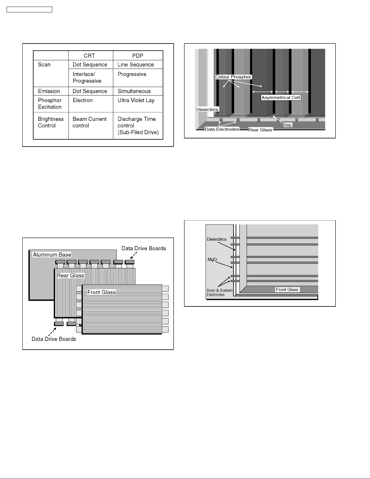
Fig. A
Panasonic 42 inch wide plasma display panel is develope for
large screen multimedia display with space saving.
The plasma display panel use AC type Sub-field drive system
with Dual scanning system.
This panel have also Panasonic original Asymmetric cell and
Plasma AI technology.
Fig. A Is the CRT and Plasma Display Panel(PDP) comparison
chart.
1.3. Rear Glass Structure
Fig. C
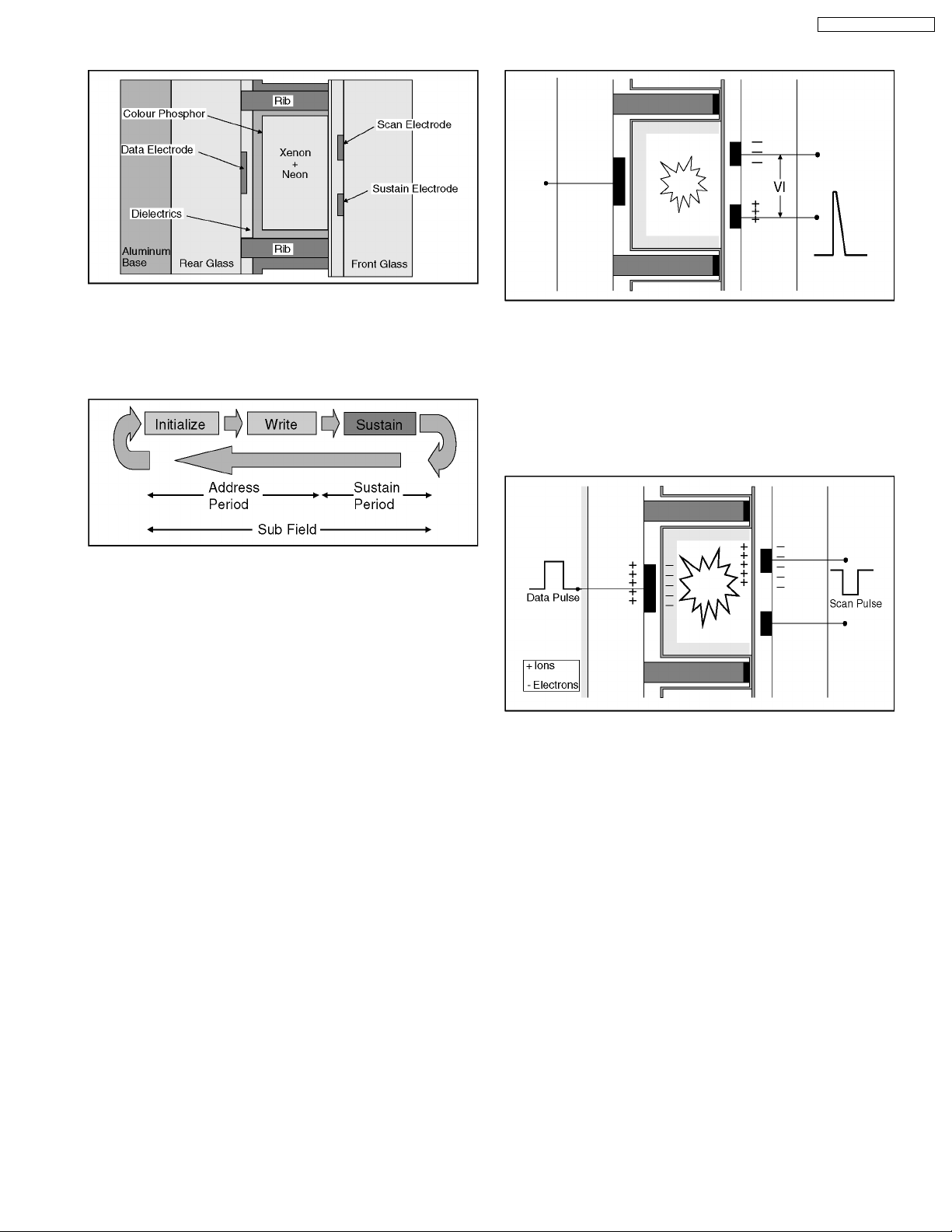
On the rear glass the data electrode is mounted.
The dielectric is coated on the rear glass.
Red, Green and Blue colour phosphors are formed on the data
electrode with the ribs. However to improve colour reproduction
and brightness, each colour phosphors are formed different
width This is called " Asymmetrical cell " as Panasonic original
technology.
1.4. Front Glass Structure
1.2. Plasma display panel structure
Fig. B
Plasma display panel structure
Panasonic Plasma display panel is consist of front glass, rear
glass and Aluminum base.
The front glass has each 768 lines scan and sustain
transparence electrodes.
The rear glass has 4098 (1366 x 3 ) data electrodes on the
inner surface. These electrodes are connected to the data drive
circuit boards directory.
Fig. D
On the front glass scan and sustain transparent electrodes are
mounted in pair.
The dielectrics is coated on the front grass.
MgO over coat is also applied on the dielectrics.
The front and rear glasses are piled and sealed . And low
presser gas are charged between two glasses.
4
Page 5
1.5. Pixel Structure
Fig. E
50 inch plasma display panel has 1,049,088 pixels.
Each pixels structure is shown fig. E.
1.6. Sub Field Drive system
TH-50PHD3 / TH-50PHW3
1.7. Initialization
Fig. G
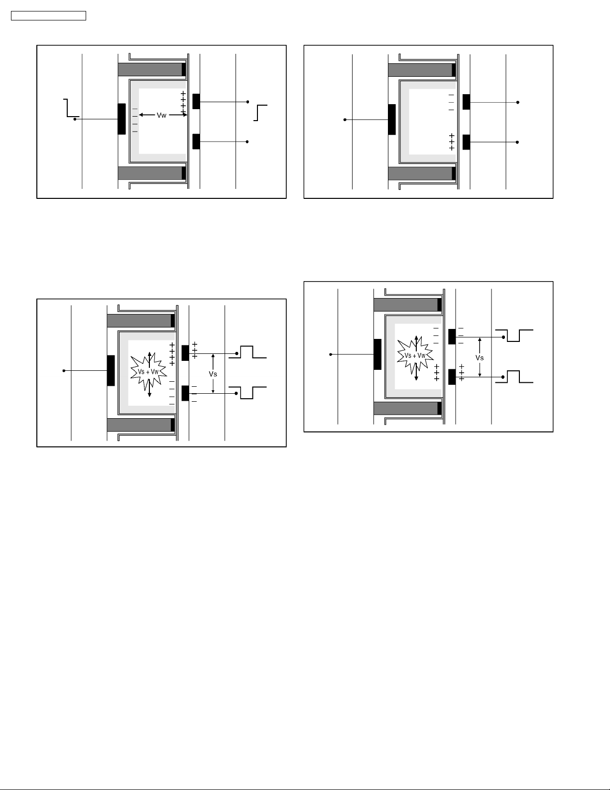
To clear any remaining electric charge into the pixel, trapezoid
voltage is applied between the scan and sustain electrodes.
Plasma discharge is started but the discharge become small
gradually.
Then any electric charge is cleared.
1.8. Write
Fig. F
Brightness control of plasma display panel is carried out by
plasma discharge time change. To control each pixelís
brightness Sub-field drive system is used.
A sub-field is consist of Initialize, Write and sustain operation.
Fig. H
Data Pulse which is positive polarity is input to data electrode
and Scan pulse which is negative polarity is input to scan
electrode simultaneously.
That means sum of data and scan pulses voltage is applied
between two electrodes as discharge start voltage.
Discharge is started into the pixel and gas is ionized.
During discharging Ion is charged on the scan electrode side
and electron is charged on data electrode side.
5
Page 6
TH-50PHD3 / TH-50PHW3
1.9. Wall Voltage
1.11. Sustain Step 2
Fig. I
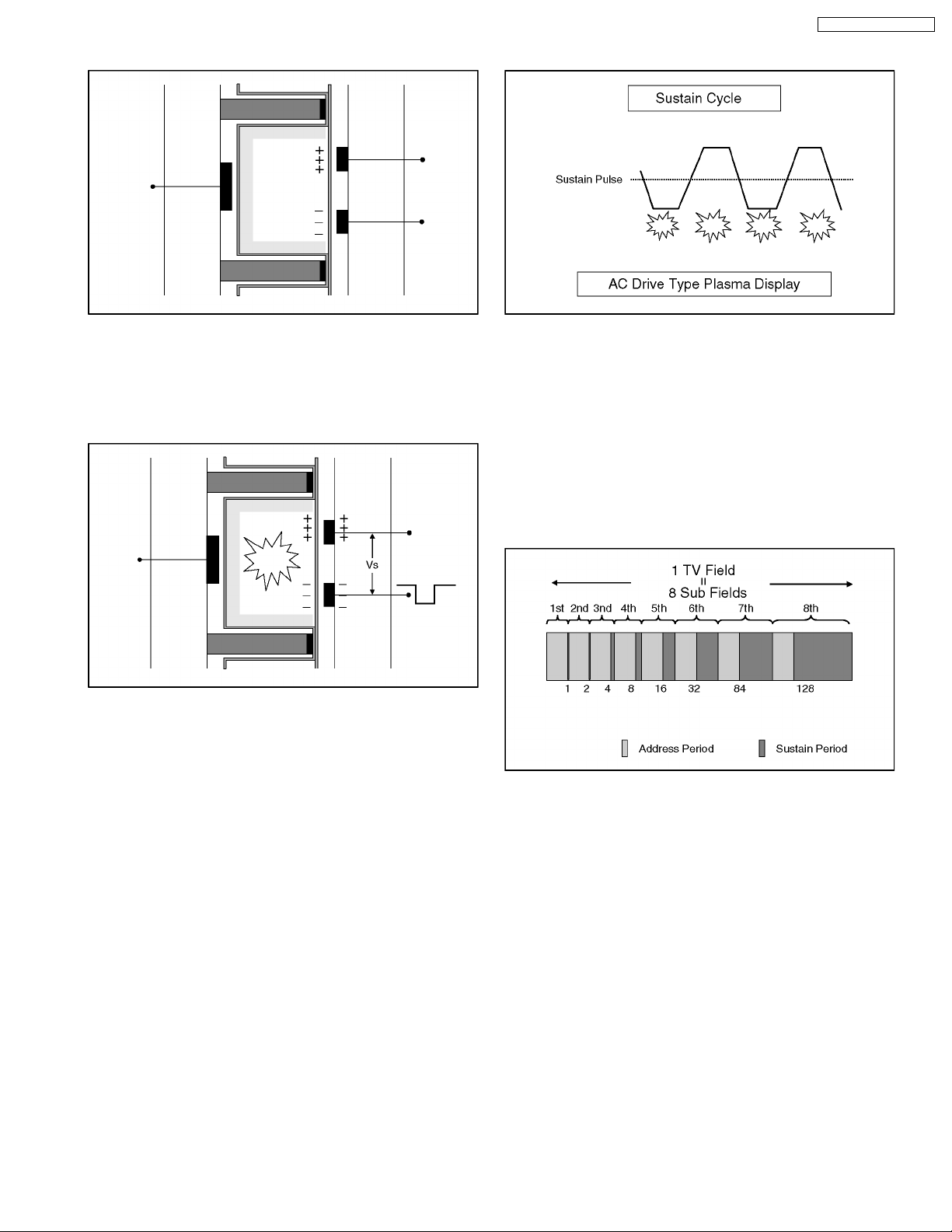
When input pulses are stopped, Ions and Electrons which are
charged on the dielectric around the electrodes are remained.
This charge is called Wall Voltage (Pilot voltage).
This operation is called Write .
1.10. Sustain Step 1
Fig. J
Negative polarityís Sustain pulse is input between sustain and
scan electrodes and voltage potential between two electrodes
becomes sum of Sustain pulse and wall voltage.
Then discharge start.
Fig. K
When sustain pulse is stopped, Ions and Electrons are
remained again as Wall voltage. However polarity of wall
voltage is reversed.
1.12. Sustain Step 3
Fig. L
Positive polarity´s Sustain pulse is input between sustain and
scan electrodes and discharge start again.
6
Page 7
1.13. Sustain Step 4
TH-50PHD3 / TH-50PHW3
1.15. Repeat Step 1 to Step 5
Fig. M
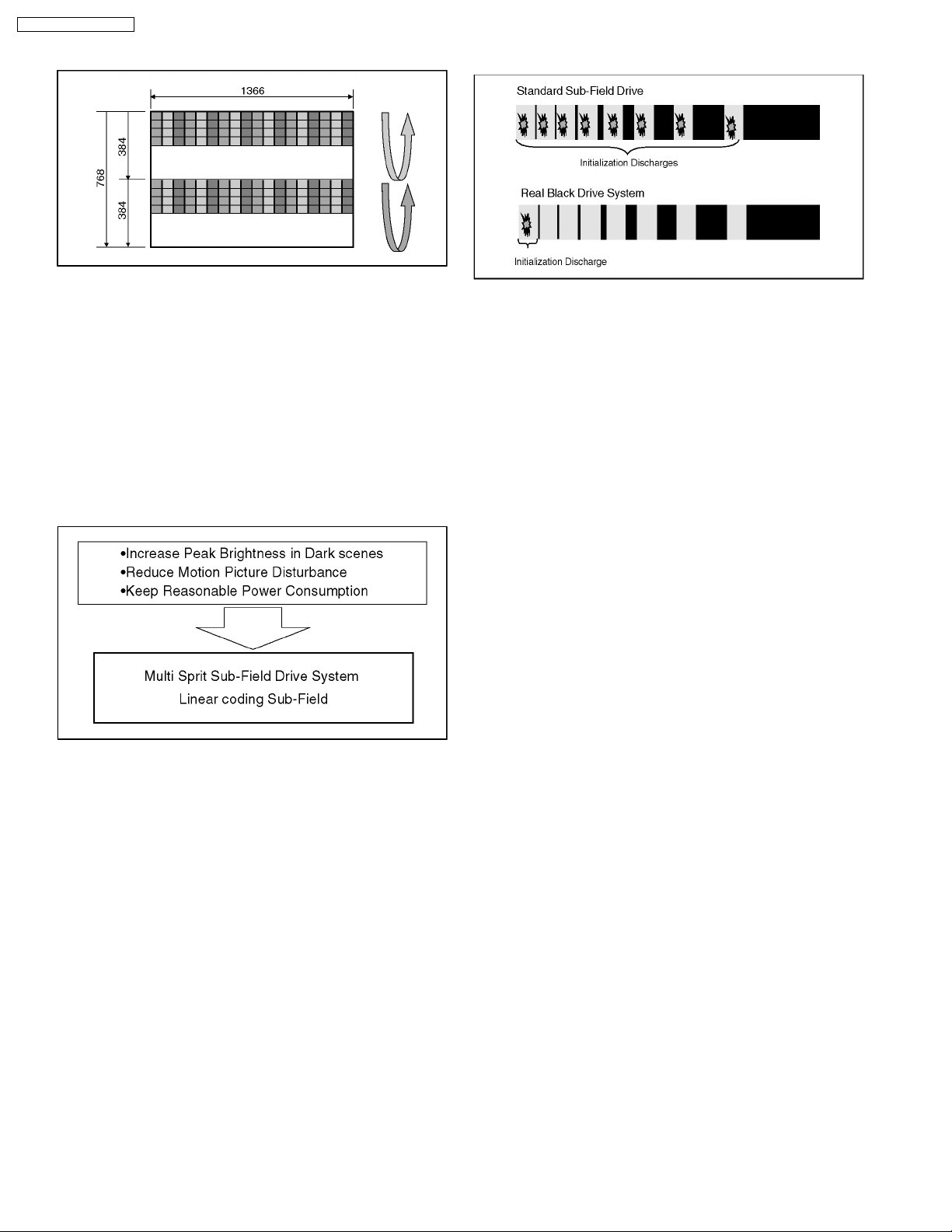
When sustain pulse is stopped, Ions and Electrons are
remained again as Wall voltage. However polarity of wall
voltage is reversed.
1.14. Sustain Step 5
Fig. N
Ions and Electrons which is generated by 2nd sustain
discharge are charged on the pixel wall(dielectric) around the
electrodes.
Fig. O
To keep discharge continuously step 1 to 5 operation will be
repeated.
As the result sustain pulse is alternated. Therefore we call this
drive system AC Drive type.
If sustain operation is repeated longer, brightness level of the
pixel is increased. Therefore depend on sustain discharge time
brightness of pixel is controlled.
1.16. Sub-Field drive
Fig. P
Sub-Field drive is PDP unique system.
While one TV field period, 8 bits digital video signal component
is reproduced by 8 sub-fields operation.
Each Sub-Field´s address period are all same.(Consist of one
initialization and 768 scanning operation)
But Sustain period of each Sub-Field are different.1st SubField(SF) reproduce only 1 step brightness.
2nd SF reproduce 2 steps brightness.
Each sub-field´s sustain period are increased gradually.
However total 256 brightness difference can be reproduced on
the screen.
7
Page 8
TH-50PHD3 / TH-50PHW3
1.17. Dual Scan
1.19. Real Black drive
Fig. Q
The sustain period of sub-field drive system. Therefore
brightness peak is limited. Because 768 horizontal lines
scanning is carried out during address period.
Dual scan system can reduce scanning time from 768 to 384 in
the address period.
Then spaced time by dual scanning can be used for sustain
operation.
As the result Brightness peak level can be increased.
1.18. Plasma AI (Adaptive
brightness Intensifier)
Fig. S
For standard sub field drive, initialization discharge is done at
each sub field. So that during one TV field period same sub
field numbers of discharges are done even black signal was
displayed.
Therefore there are small emission at the black area.
Panasonic Real Black drive system improve black
reproduction.
Initialization discharge is done at first sub field only.
Remaining sub field are not required discharge because Real
Black drive circuit applies initialization electric field remainder
pulse.
Fig. R
Panasonic plasma AI control sub-field drive operation which is
called Multi-Sprit Sub-Field drive control system.
Depend on the picture contents ( APL : Average Picture Level
) sustain time format of each sub-field are also rearranged from
binary format to linear cording sustain time. (Linear coding subfield)
Plasma AI select the best display condition for Plasma display
panel to display natural and crisp picture.
8
Page 9
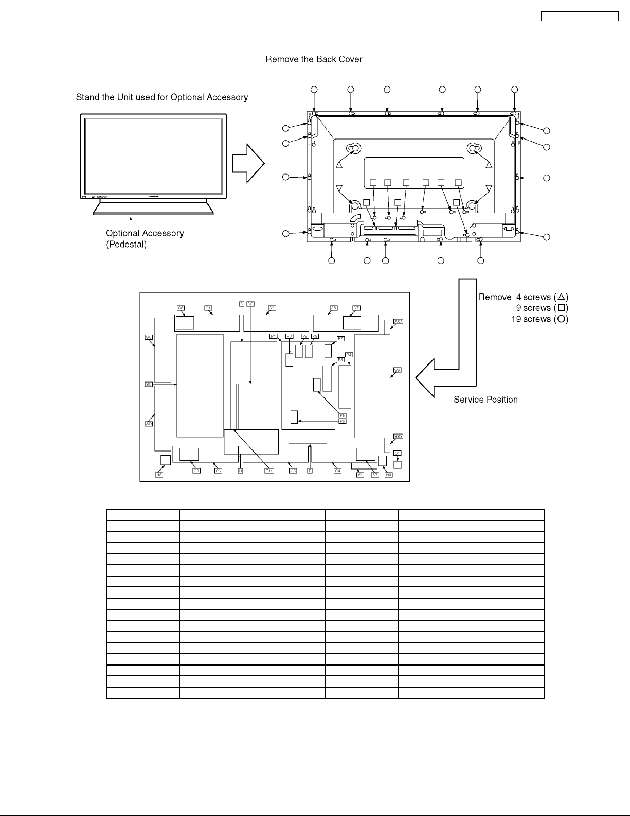
2 Service Hint
TH-50PHD3 / TH-50PHW3
Baord name Function Board name Function
C1 Data drive (Upper Left) P4 Panel drive power
C2 Data drive (Upper Center) P5 Processing voltage control
C3 Data drive (Upper Right) P6 PFC oscillator
C4 Data drive (Lower Left) P7 High Voltage protect
C5 Data drive (Lower Center) P8 Low Voltage protect
C6 Data drive (Lower Right) P9 Regulator
C7 Saving power S1 Power switch
C8 Saving power SC Scan drive
D Digital process & control SD Scan drive output (Lower)
DG RGB/IF SS Sustain drive
F Line Filter SS2 Sustain conne ction (Upper)
F Line Filter SS3 Sustain conne ction (Lower)
H Rear terminal SU Scan drive output (Upper)
H3 Speaker terminal T11 Interface
P1 Power supply V1 Front switch & Remote Receiver
P3 Sustain voltage control
9
Page 10
TH-50PHD3 / TH-50PHW3
3 Adjustment Procedure
3.1. +B Set-up
3.1.1. Item / Preparation
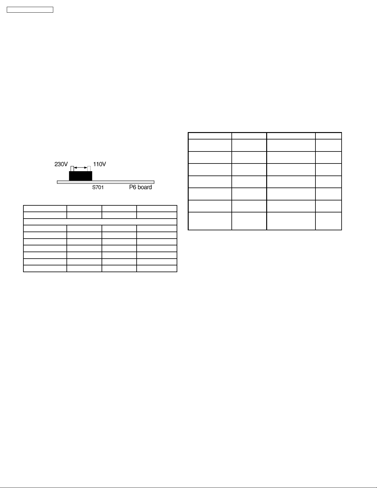
1. Confirm the main voltage set switch Is set to 230V. (A, B,
and E version) Confirm the main voltage set switch is set to
110V. (U version)
Note:
230V covers input AC voltage from 200V till 260V, and
110V covers from 90V till 130V.
2. Input a Grey scale signal.
3. Set the picture controls: -
Picture mode: Normal
White balance: Normal
3.1.2. Adjustments
Adjust and confirm indicated test point for the specified voltage.
Test point Voltage Volume Name
P4 pin 1 (Hot) 400V ±1V R548 PFC
Confirmation (Cold)
P27 pin 5 16V ±0.5V +15V
D5 pin 1 14V ±0.5V +13.5V
DG6 pin 1 14V ±0.5V Audio15V
DG6 pin 3 -14V ±0.5V Audio-15V
D5 pin 5 5.2V ±0.3V +5.25V
D5 pin 8 3.6V ±0.2V +3.65V
D7 pin 4 5V ±0.3V STB5V
3.2. Driver Set-up
3.2.1. Item / Preparation
1. Input an APL 100 % white signal.
2. Set the picture controls: -
Picture mode: Normal
White balance: Cool
Aspect: 16:9
3.2.2. Adjustments
Adjust driver section voltages referring the panel data on the
panel data label.
Test point Voltage Volume Name
TPVSUS
(SS-BOARD)
TPVBK
(SC-BOARD)
TPVE
(SS-BOARD)
TPVSET
(SC-BOARD)
TPVAD
(SC-BOARD)
P27 pin2 (P1BOARD
Between TPVscn
and TPVAD
(SC-BOARD)
VSUS ±1V R639(P3-BOARD) Vsus
140 V ±5V R513(P1-BOARD) Vbk
VE ±0.5V R6829(SS-BOARD) Ve
224 V ±1V R6490(SC-BOARD) Vset
VAD ±1V R960(P4-BOARD) Vad
75 V ±0.5V R528 (P1-BOARD) Vda
120 + (Vad)
±0.5V
R967 (P4-BOARD) Vscan
10
Page 11
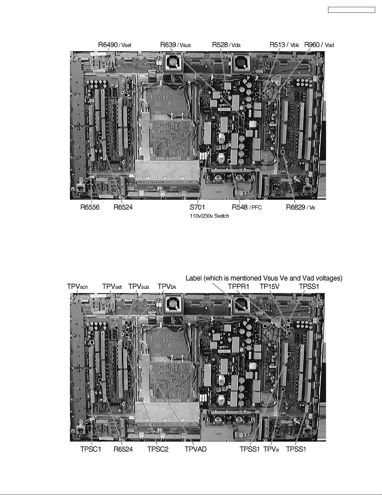
3.3. Adjustment Volume Location
TH-50PHD3 / TH-50PHW3
3.4. Test Point Location
11
Page 12
TH-50PHD3 / TH-50PHW3
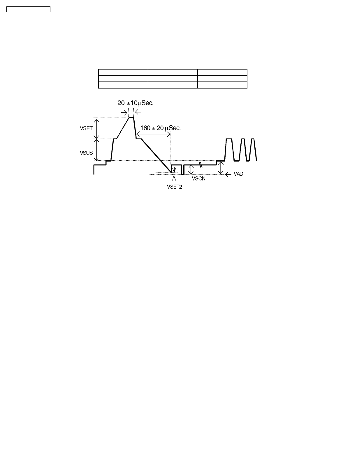
3.5. Initialization Pulse Adjust
1. Input a Cross hatch signal.
2. Set the picture controls: -
Picture mode: Normal
White balance: Cool
Adjust the indicated test point for the specified wave form.
Test point Volume
TPSC1 (SC) R6524 (SC) 20±10µ Sec
TPSC1 (SC) R6556 (SC) 160±20µ Sec
12
Page 13
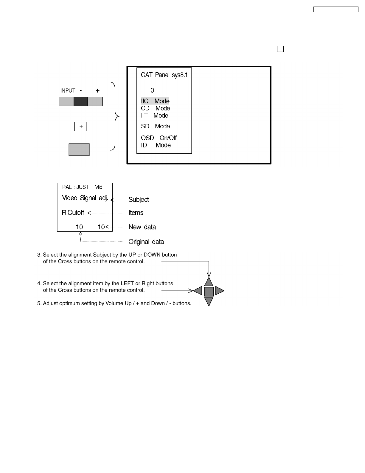
4 Alignment Setting
4.1. How to access Alignment
TH-50PHD3 / TH-50PHW3
1. Press and hold the
control 3 times quickly within 1 second, this will place the unit into the CAT menu (Main service mode)
2. Press the Access button on the remote control.
Volume down / -
button on the front panel of the unit and press the
status [ +
]
button on the remote
4.2. Exit
1. To exit the
2. To exit the
CAT mode
IIC mode
, press theRbutton on the remote control.
, access the
ID mode
by the down button of cross buttons and switch off the main power and on again.
13
Page 14
TH-50PHD3 / TH-50PHW3
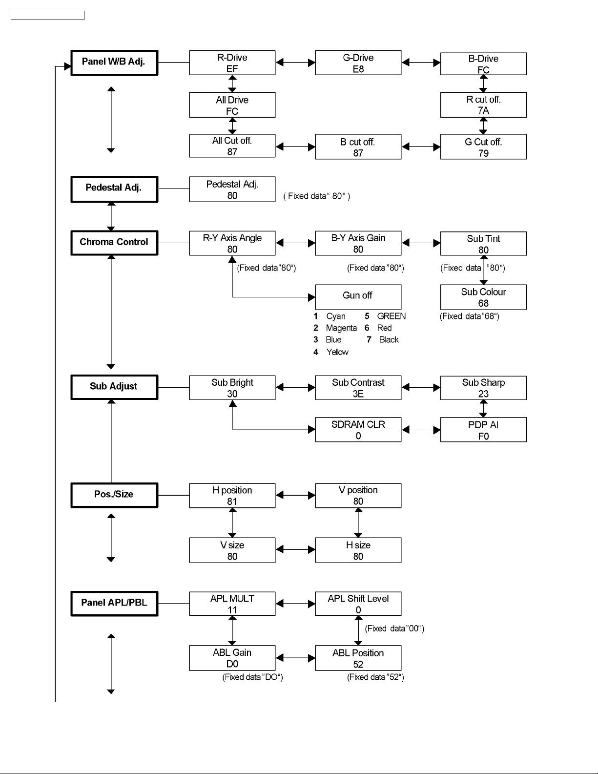
4.3. IIC menu structure
14
Page 15
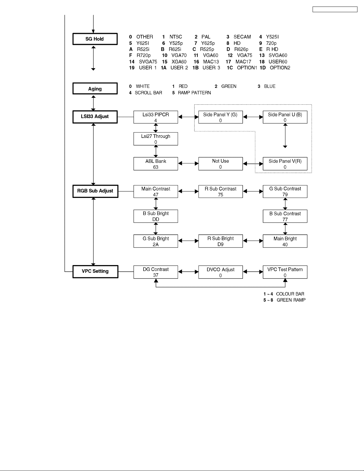
TH-50PHD3 / TH-50PHW3
15
Page 16
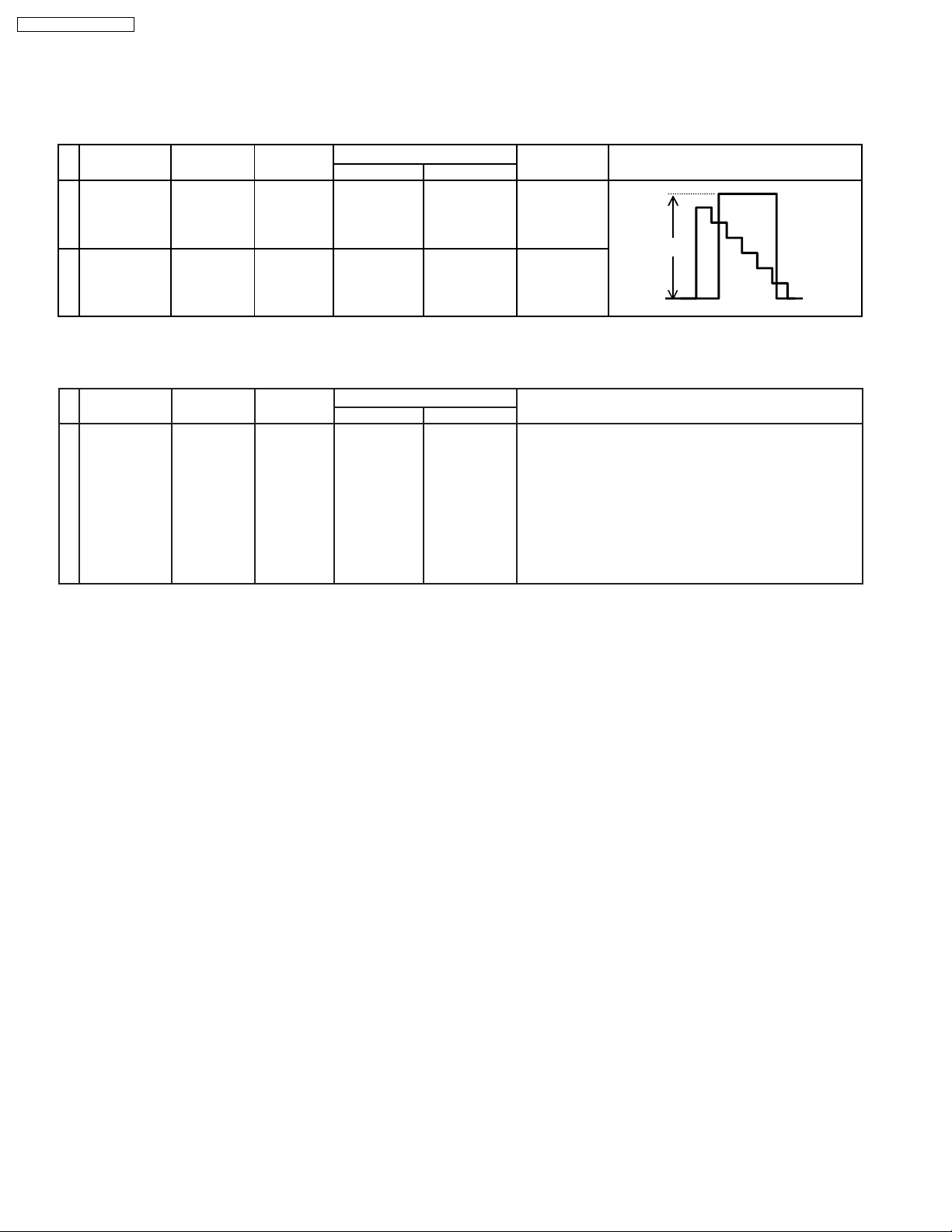
TH-50PHD3 / TH-50PHW3
5 Alignment
5.1. DG contrast
(Composit video signal)
INPUT Equipment Test Point Level Remark
Alignment menu
Subject Item
1 NTSC Oscilloscope TP8004 VPC SETTING
Colour Bar
2 PAL Oscilloscope TP8004 VPC SETTING
Colour Bar
(DG Boad)
(DG Board)
5.2. DVCO adjust
Alignment menu
Subject Item
1 NTSC or PAL - - VPC SETTING
Colour Bar
Standard signal
DG CONTRAST
DG CONTRAST
DVCO SETTING
0.7V+-0.02V
(3A)
100IRE
0.55V+-0.02V
(3A)
ProcedureINPUT Equipment Test Point
1) Access to DVCO SETTING mode.
2) Press ACCESS key on remote then automatic
DVCO setting is started.
3) When data becomes " 1 "adjustment is completed. .
* Do not use this function without input signal.
16
Page 17
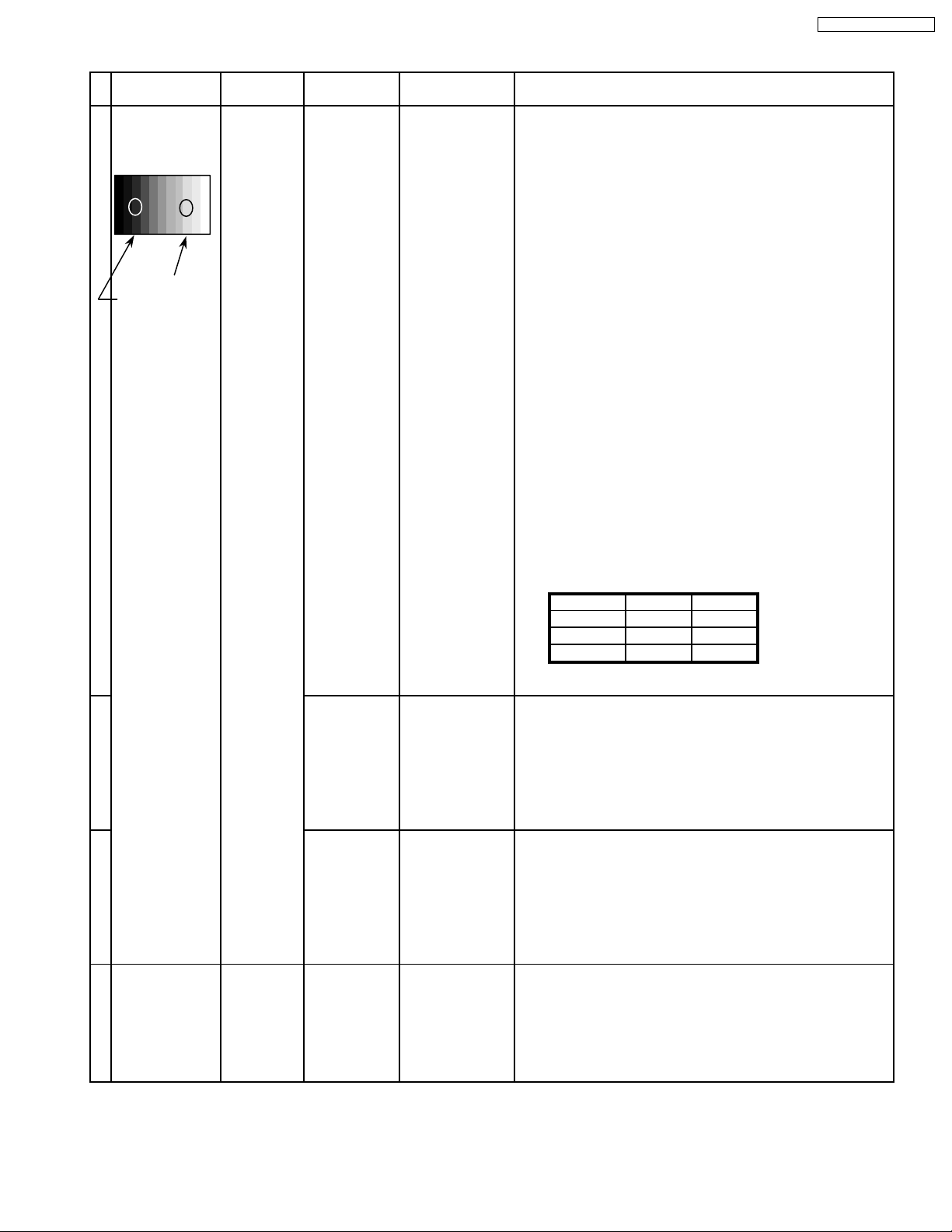
5.3. NTSC panel white balance
INPUT Alignment menu ProcedureEquipment Setting
1 NTSC Color Picture: 1) Find the nearest area to brightness of 10 cd/m2 as Low
Gray Scale Analyzer Normal Sub Adjust light by color sensor.
Pattern White balance: Sub Bright 2) Adjust Sub bright to set Low light level to 10 cd/m
Cool exactly.
Aspect: PANEL W/B
16:9 G cut off 3) Set G cut off to " 80 ".
PANEL W/B
B cut off 4) Adjust B and R cut off to set color temperature as
R cut off shown Fig.-01.
High light 75% Sub Adjust
Low light 15% Sub Bright 5) If Sub Bright is changed re-adjust it to set Low light
to 10 cd/m
6)Find 75% of white area by color sensor.
PANEL W/B
G Drive 7) Set G Drive to " D8 ".
PANEL W/B
B Drive 8) Adjust B and R Drive to set color temperature
R Drive as shown Fig.-01.
9) Repeat item 4) to 7) to set both Low light and
high light.
PANEL W/B
R,G,B Drive 10) Increase same steps of R, G and B Drive to set
R,G,B Drive largest level of 3 color drive to "FC".
PANEL W/B
R,G,B cut off 11) Re-adjust Low light level again.
2
.
TH-50PHD3 / TH-50PHW3
2
Color Temp. x y
Cool(Hi) 0.272 0.290
Normal(Mid) 0.288 0.296
Warm(Low) 0.313 0.329
Fig. -01
2 Picture: 1) Change white balance to "Normal".
Normal PANEL W/B
White balance: R,G,B cut off 2) Repeat procedure 3) to 11) of Cool mode.
Normal PANEL W/B
Aspect: R,G,B Drive
16:9
3 Picture: 1) Change white balance to "Normal".
Normal PANEL W/B
White balance: R,G,B cut off 2) Repeat procedure 3) to 11) of Cool mode.
Warm PANEL W/B
Aspect: R,G,B Drive
16:9
4 Picture: Picture Menu 1) Change color templature to "Cool".
Normal Sub Adjust
White balance: Sub Bright 2)Re-set Sub bright to "30"
Cool
Aspect:
16:9
17
Page 18
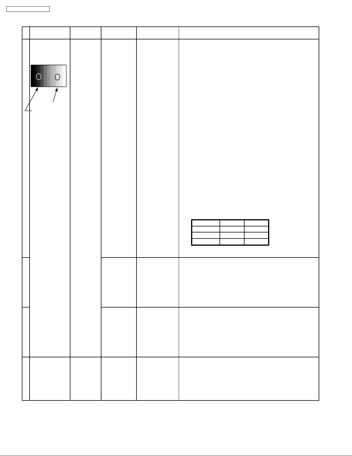
TH-50PHD3 / TH-50PHW3
5.4. PAL/SECAM panel white balance
INPUT Alignment menu ProcedureEquipment Setting
1 PAL Color Picture: 1) Find the nearest area to brightness of 10 cd/m2 as Low
Gray Scale Analyzer Normal Sub Adjust light by color sensor.
Pattern White balance: Sub Bright 2) Adjust Sub bright to set Low light level to 10 cd/m
Cool exactly.
Aspect: PANEL W/B
16:9 G cut off 3) Set G cut off to " 80 ".
PANEL W/B
High light 75% Sub Adjust
Low light 15% Sub Bright 5) If Sub Bright is changed re-adjust it to set Low light
PANEL W/B
PANEL W/B
PANEL W/B
PANEL W/B
B cut off 4) Adjust B and R cut off to set color temperature as
R cut off shown Fig.-02.
to 10 cd/m
2.
6)Find 75% of white area by color sensor.
G Drive 7) Set G Drive to " D8 ".
B Drive 8) Adjust B and R Drive to set color temperature
R Drive as shown Fig.-02.
9) Repeat procedure 4) to 7) to set both Low light and
high light.
R,G,B Drive 10) Increase same steps of R, G and B Drive to set
R,G,B Drive largest level of 3 color drive to "FC".
R,G,B cut off 11) Re-adjust Low light level again.
2
Color Temp. x y
Cool(Hi) 0.272 0.290
Normal(Mid) 0.288 0.296
Warm(Low) 0.313 0.329
Fig. -02
2 Picture: 1) Change white balance to "Normal".
Normal PANEL W/B
White balance: R,G,B cut off 2) Repeat procedure 3) to 11) of Cool mode.
Normal PANEL W/B
Aspect: R,G,B Drive
16:9
3 Picture: 1) Change white balance to "Normal".
Normal PANEL W/B
White balance: R,G,B cut off 2) Repeat procedure 3) to 11) of Cool mode.
Warm PANEL W/B
Aspect: R,G,B Drive
16:9
4 Picture: Picture Menu 1) Change color templature to "Cool".
Normal Sub Adjust
White balance: Sub Bright 2)Re-set Sub bright to "30"
Cool
Aspect:
16:9
18
Page 19
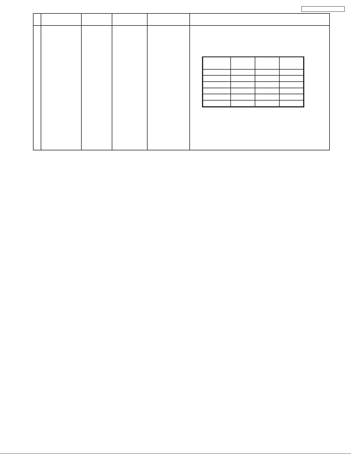
TH-50PHD3 / TH-50PHW3
Alignment menu ProcedureEquipment Setting
5 Picture: 1) Write down each color temaparature of R,G,B drive and
Normal Cut off data as follows.
Aspect:
16:9
White
White balance:
Cool
Normal
Warm
Balance Cool Normal Warm
R Drive
G Drive
B Drive
R Cut off
G Cut off
B Cut off
SECAM signal 2) Input SECAM signal.
3) Copy PAL R,G,B drive and cut off data of each white
balance mode to SECAM position.
19
Page 20
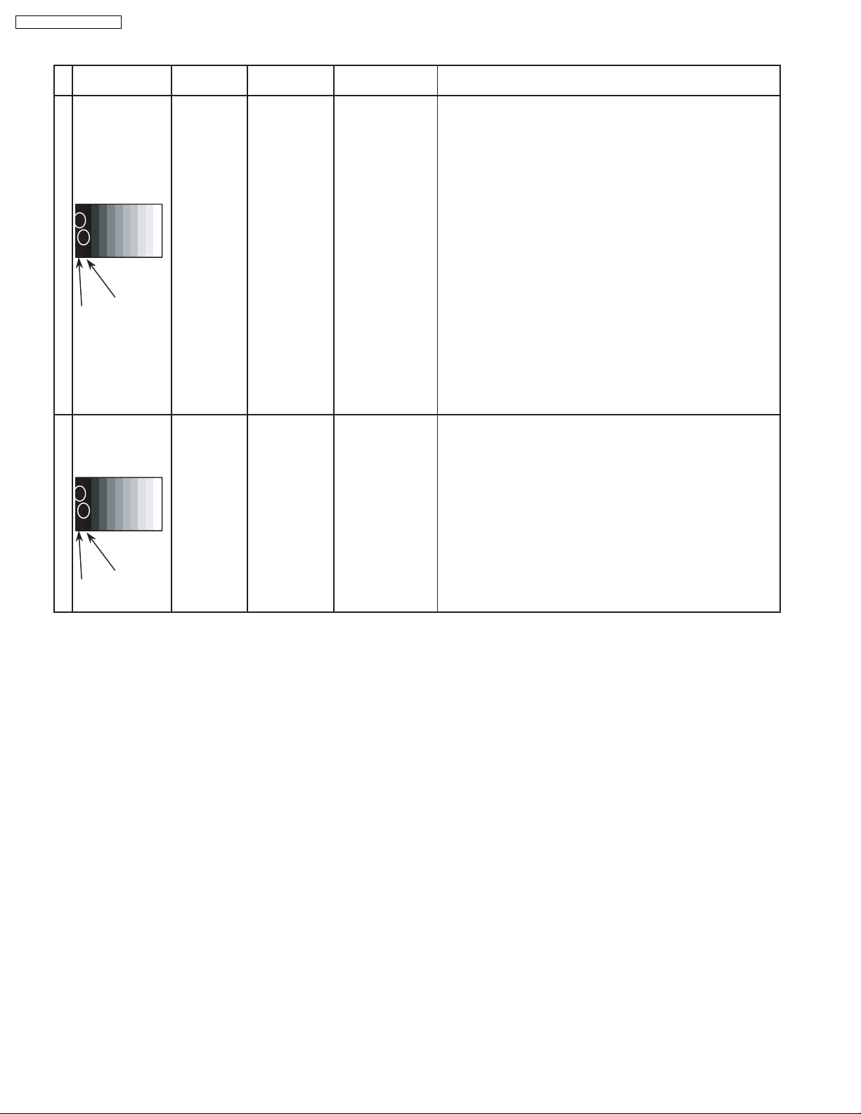
TH-50PHD3 / TH-50PHW3
5.5. Pedestal setting
INPUT Alignment menu ProcedureEquipment Setting
1 Component Picture: PANEL W/B
(525i, 525p, 625i, Normal R cut off 1) Set R,G and B cut off to "
720i or 1080i) White balance: G cut off
Gray Scale Aspect:
Pattern 16:9
Black 2 %
Black 0 % at black 2% area and no emission at black 0% area.
Cool B cut off
Chroma Control:
Gun off
RGB Sub Adjust:
G Sub Bright
Chroma Control:
Gun off
RGB Sub Adjust:
B Sub Bright
Chroma Control:
Gun off
RGB Sub Adjust:
R Sub Bright
** Adjust at the dark room.
80 ".
2) Set Gun off to "
3) Adjust G Sub bright to start some of green pixels emission
at black 2% area and no emission at black 0% area.
4) Set Gun off to "
5) Adjust B Sub bright to start some of blue pixels emission
6) Set Gun off to "
7) Adjust R Sub bright to start some of red pixels emission
at black 2% area and no emission at black 0% area.
5". (Only green pixels can emit.)
3". (Only blue pixels can emit.)
6". (Only red pixels can emit.)
2 RGB(PC) Picture: 1) Change input to RGB signal.
Gray Scale Normal PANEL W/B
Pattern White balance: R,G,B cut off 2) Repeat procedure 1) to 7) of Component input signal.
Cool PANEL W/B
Aspect: R,G,B Drive
16:9
Black 2 %
Black 0 %
20
Page 21
5.6. PC/RGB panel white balance
INPUT Alignment menu ProcedureEquipment Setting
1 PC Color Picture: 1) Find the nearest area to brightness of 10 cd/m2 as Low
Gray Scale Analyzer Normal Sub Adjust light by color sensor.
Pattern White balance: Sub Bright 2) Adjust Sub bright to set Low light level to 10 cd/m
Cool exactly.
Aspect: PANEL W/B
16:9 G cut off 3) Set G cut off to " 80 ".
PANEL W/B
B cut off 4) Adjust B and R cut off to set color temperature as
R cut off shown Fig.-03.
High light 75% Sub Adjust
Low light 15% Sub Bright 5) If Sub Bright is changed re-adjust it to set Low light
to 10 cd/m
6)Find 75% of white area by color sensor.
PANEL W/B
G Drive 7) Set G Drive to " D8 ".
PANEL W/B
B Drive 8) Adjust B and R Drive to set color temperature
R Drive as shown Fig.-03.
9) Repeat item 4) to 7) to set both Low light and
high light.
PANEL W/B
R,G,B Drive 10) Increase same steps of R, G and B Drive to set
R,G,B Drive largest level of 3 color drive to "FC".
PANEL W/B
R,G,B cut off 11) Re-adjust Low light level again.
2
.
TH-50PHD3 / TH-50PHW3
2
Color Temp. x y
Cool(Hi) 0.272 0.290
Normal(Mid) 0.288 0.296
Warm(Low) 0.313 0.329
Fig. -03
2 Picture: 1) Change white balance to "Normal".
Normal PANEL W/B
White balance: R,G,B cut off 2) Repeat procedure 3) to 11) of Cool mode.
Normal PANEL W/B
Aspect: R,G,B Drive
16:9
3 Picture: 1) Change white balance to "Normal".
Normal PANEL W/B
White balance: R,G,B cut off 2) Repeat procedure 3) to 11) of Cool mode.
Warm PANEL W/B
Aspect: R,G,B Drive
16:9
4 Picture: Picture Menu 1) Change color templature to "Cool".
Normal Sub Adjust
White balance: Sub Bright 2)Re-set Sub bright to "30"
Cool
Aspect:
16:9
21
Page 22
TH-50PHD3 / TH-50PHW3
INPUT Alignment menu ProcedureEquipment Setting
5 Picture: 1) Write down each color temaparature of R,G,B drive and
RGB
Gray Scale
Pattern
High light 75%
Low light 15% 3) Copy PC R,G,B drive and cut off data of each white
Normal Cut off data as follows.
Aspect:
16:9
White balance:
Cool
Normal
Warm
White
Balance Cool Normal Warm
R Drive
G Drive
B Drive
R Cut off
G Cut off
B Cut off
2) Input RGB signal.
balance mode to RGB position.
22
Page 23
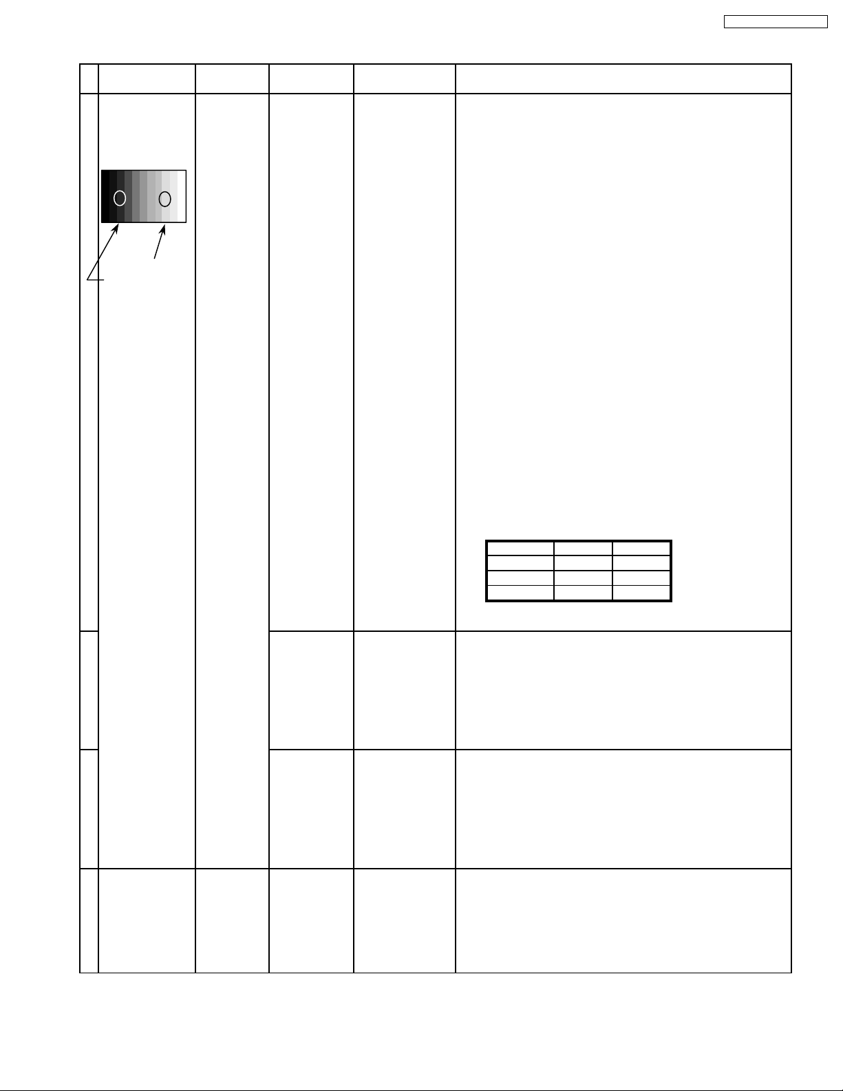
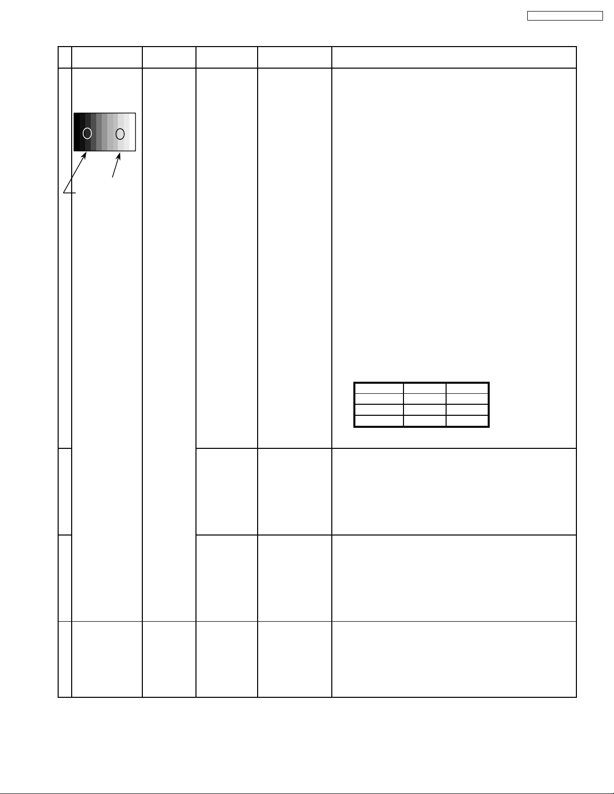
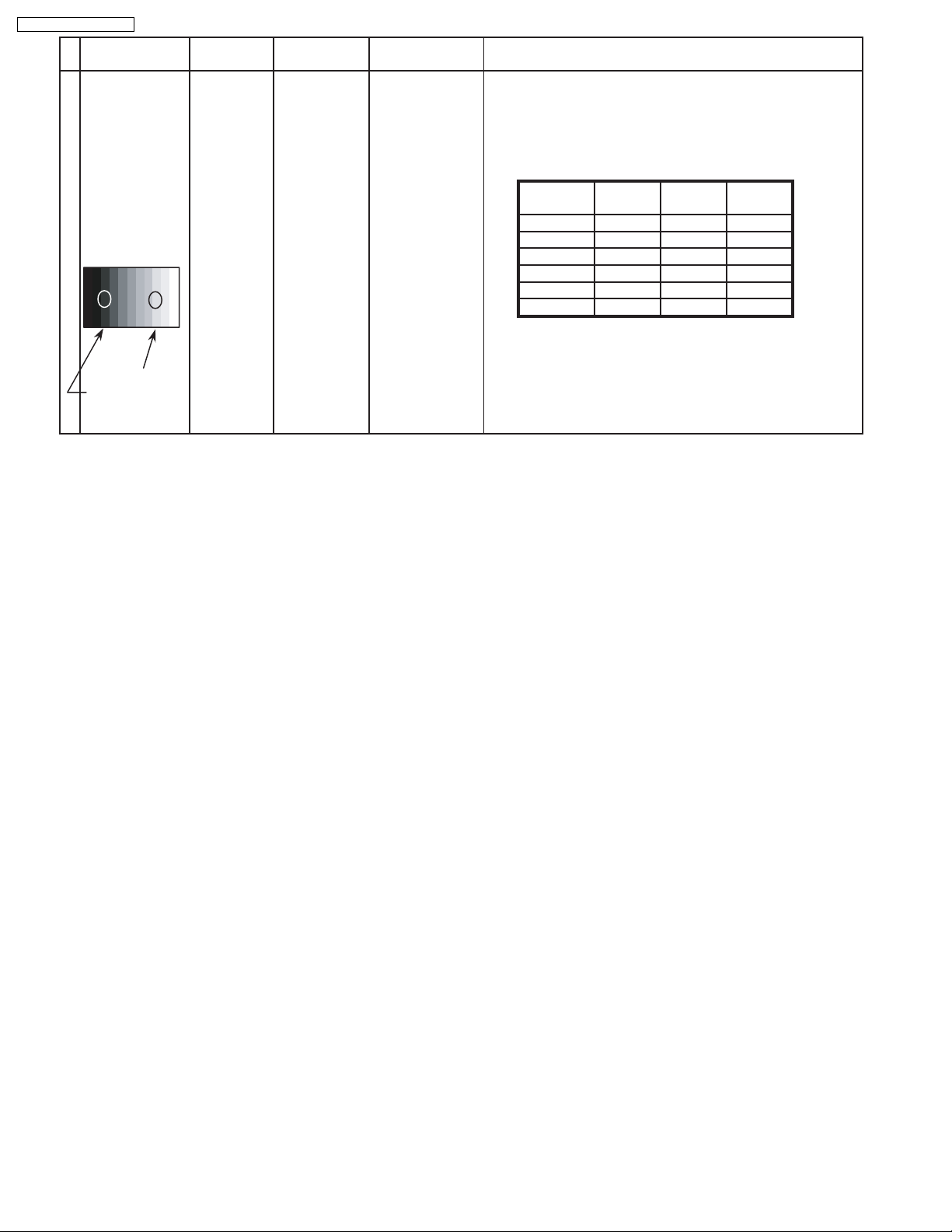
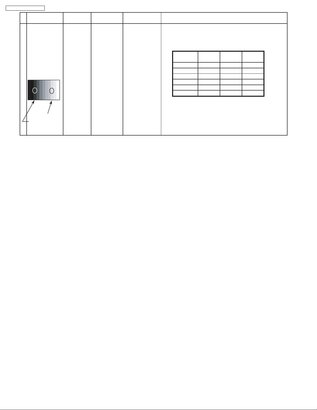
5.7. HD/ 525i /525p panel white balance
INPUT Alignment menu ProcedureEquipment Setting
1HD(720i or 1080i) Color Picture: 1) Find the nearest area to brightness of 10 cd/m2 as Low
Gray Scale Analyzer Normal Sub Adjust light by color sensor.
Pattern White balance: Sub Bright 2) Adjust Sub bright to set Low light level to 10 cd/m
Cool
Aspect: PANEL W/B
16:9 G cut off 3) Set G cut off to " 80 ".
PANEL W/B
B cut off 4) Adjust B and R cut off to set color temperature as
R cut off shown Fig.-04.
High light 75% Sub Adjust
Low light 15% Sub Bright 5) If Sub Bright is changed re-adjust it to set Low light
PANEL W/B
G Drive 7) Set G Drive to " D8 ".
PANEL W/B
R Drive as shown Fig.-04.
exactly.
2
to 10 cd/m
.
6)Find 75% of white area by color sensor.
B Drive 8) Adjust B and R Drive to set color temperature
TH-50PHD3 / TH-50PHW3
2
9) Repeat item 4) to 7) to set both Low light and
high light.
PANEL W/B
R,G,B Drive 10) Increase same steps of R, G and B Drive to set
R,G,B Drive largest level of 3 color drive to "FC".
PANEL W/B
R,G,B cut off 11) Re-adjust Low light level again.
Color Temp. x y
Cool(Hi) 0.272 0.290
Normal(Mid) 0.288 0.296
Warm(Low) 0.313 0.329
Fig. -04
2 Picture: 1) Change white balance to "Normal".
Normal PANEL W/B
White balance: R,G,B cut off 2) Repeat procedure 3) to 11) of Cool mode.
Normal
PANEL W/B
Aspect: R,G,B Drive
16:9
3 Picture: 1) Change white balance to "Normal".
Normal PANEL W/B
White balance: R,G,B cut off 2) Repeat procedure 3) to 11) of Cool mode.
Warm
PANEL W/B
Aspect: R,G,B Drive
16:9
4 Picture: Picture Menu 1) Change color templature to "Cool".
Normal Sub Adjust
White balance: Sub Bright 2)Re-set Sub bright to "30"
Cool
Aspect:
16:9
23
Page 24
TH-50PHD3 / TH-50PHW3
INPUT Alignment menu ProcedureEquipment Setting
5 Picture: 1) Write down each color temaparature of R,G,B drive and
RGB
Gray Scale
Pattern
High light 75%
Low light 15% 3) Copy HD drive and cut off data of each white
Normal Cut off data as follows.
Aspect:
16:9
White balance:
Cool
Normal
Warm
White
Balance Cool Normal Warm
R Drive
G Drive
B Drive
R Cut off
G Cut off
B Cut off
2)Change input signal to 525i and 525p.
balance mode to each signals position.
24
Page 25
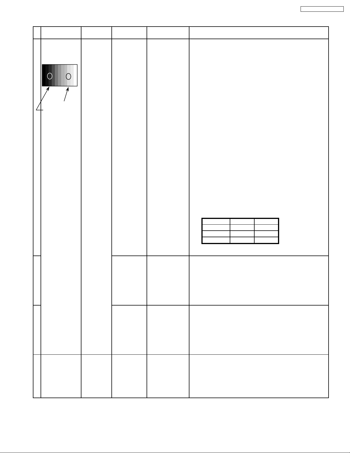
5.8. 625i panel balance
INPUT Alignment menu ProcedureEquipment Setting
1 625i Color Picture: 1) Find the nearest area to brightness of 10 cd/m2 as Low
Gray Scale Analyzer Normal Sub Adjust light by color sensor.
Pattern White balance: Sub Bright 2) Adjust Sub bright to set Low light level to 10 cd/m
Cool exactly.
Aspect: PANEL W/B
16:9 G cut off 3) Set G cut off to " 80 ".
PANEL W/B
B cut off 4) Adjust B and R cut off to set color temperature as
R cut off shown Fig.-05.
High light 75% Sub Adjust
Low light 15% Sub Bright 5) If Sub Bright is changed re-adjust it to set Low light
to 10 cd/m
6)Find 75% of white area by color sensor.
PANEL W/B
G Drive 7) Set G Drive to " D8 ".
PANEL W/B
B Drive 8) Adjust B and R Drive to set color temperature
R Drive as shown Fig.-05.
9) Repeat item 4) to 7) to set both Low light and
high light.
PANEL W/B
R,G,B Drive 10) Increase same steps of R, G and B Drive to set
R,G,B Drive largest level of 3 color drive to "FC".
PANEL W/B
R,G,B cut off 11) Re-adjust Low light level again.
2
.
TH-50PHD3 / TH-50PHW3
2
Color Temp. x y
Cool(Hi) 0.272 0.290
Normal(Mid) 0.288 0.296
Warm(Low) 0.313 0.329
Fig. -05
2 Picture: 1) Change white balance to "Normal".
Normal PANEL W/B
White balance: R,G,B cut off 2) Repeat procedure 3) to 11) of Cool mode.
Normal PANEL W/B
Aspect: R,G,B Drive
16:9
3 Picture: 1) Change white balance to "Normal".
Normal PANEL W/B
White balance: R,G,B cut off 2) Repeat procedure 3) to 11) of Cool mode.
Warm PANEL W/B
Aspect: R,G,B Drive
16:9
4 Picture: Picture Menu 1) Change color templature to "Cool".
Normal Sub Adjust
White balance: Sub Bright 2)Re-set Sub bright to "30"
Cool
Aspect:
16:9
25
Page 26
TH-50PHD3 / TH-50PHW3
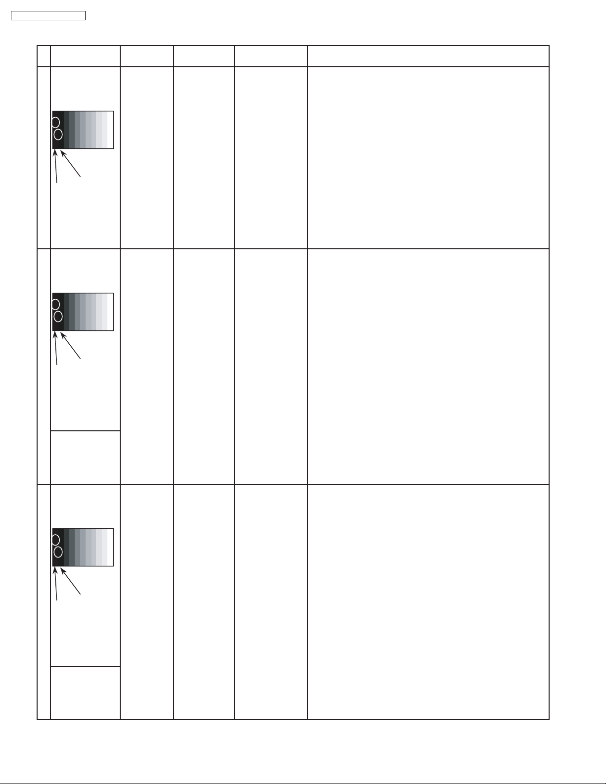
5.9. Sub brighness setting
INPUT Alignment menu ProcedureEquipment Setting
1 NTSC Picture: PANEL W/B
Gray Scale Normal All cut off 1) Set white balance to
Pattern Aspect:
** Adjust at the dark room.
Cool.
16:9 2) Adjust All cut off to start some pixels emission
at black 2% area and no emission at black 0% area.
3) Write down all cut off data.
4) Set white balance to
Black 2 %
Black 0 % 5) Adjust All cut off to set same data of Cool mode.
6) Set white balance to
7) Adjust All cut off to set same data of Cool mode.
** Adjust at the dark room.
2 PAL Picture: PANEL W/B
Gray Scale Normal All cut off 1) Set white balance to
Pattern Aspect:
16:9 2) Adjust All cut off to start some pixels emission
at black 2% area and no emission at black 0% area.
3) Write down all cut off data.
4) Set white balance to
Black 2 %
Black 0 % 5) Adjust All cut off to set same data of Cool mode.
6) Set white balance to
7) Adjust All cut off to set same data of Cool mode.
SECAM 8) Change to SECAM signal.
Gray Scale
Pattern 9) Copy PAL All cut off data to SECAM mode.
Nornal.
warm.
Cool.
Nornal.
warm.
** Adjust at the dark room.
3 PC Picture: PANEL W/B
Gray Scale Normal All cut off 1) Set white balance to
Pattern Aspect:
16:9 2) Adjust All cut off to start some pixels emission
at black 2% area and no emission at black 0% area.
3) Write down all cut off data.
4) Set white balance to
Black 2 %
Black 0 % 5) Adjust All cut off to set same data of Cool mode.
6) Set white balance to
7) Adjust All cut off to set same data of Cool mode.
RGB 8) Change to RGB input signal.
Gray Scale
Pattern 9) Copy PAL All cut off data to SECAM mode.
Cool.
Nornal.
warm.
26
Page 27
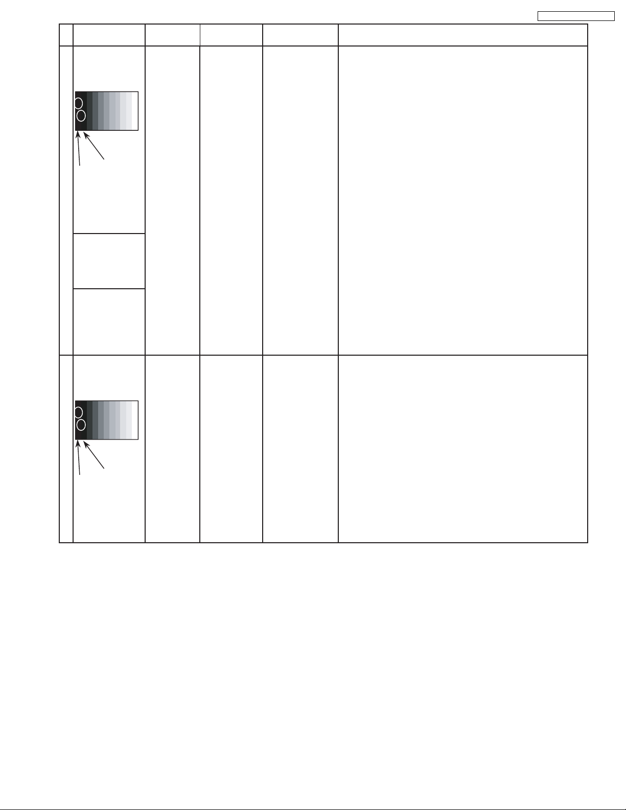
Alignment menu ProcedureINPUT Equipment Setting
** Adjust at the dark room.
4 525i Picture: PANEL W/B
Gray Scale Normal All cut off 1) Set white balance to
Pattern Aspect:
16:9 2) Adjust All cut off to start some pixels emission
at black 2% area and no emission at black 0% area.
3) Write down all cut off data.
Cool
TH-50PHD3 / TH-50PHW3
.
4) Set white balance to
Nornal
.
Black 2 %
Black 0 % 5) Adjust All cut off to set same data of Cool mode.
6) Set white balance to
warm
.
7) Adjust All cut off to set same data of Cool mode.
525p 8) Change to 525p signal.
Gray Scale
Pattern 9) Copy 525i All cut off data to 525p mode.
HD
(720i or 1080i) 8) Change to HD signal.
Gray Scale
Pattern 9) Copy 525i All cut off data to HD mode.
** Adjust at the dark room.
5 625i Picture: PANEL W/B
Cool
Gray Scale Normal All cut off 1) Set white balance to
.
Pattern Aspect:
16:9 2) Adjust All cut off to start some pixels emission
at black 2% area and no emission at black 0% area.
3) Write down all cut off data.
4) Set white balance to
Nornal
.
Black 2 %
Black 0 % 5) Adjust All cut off to set same data of Cool mode.
6) Set white balance to
warm
.
7) Adjust All cut off to set same data of Cool mode.
27
Page 28
TH-50PHD3 / TH-50PHW3
5.10. Pos./Size setting
1. Receive the test pattern signal which can be found the
center and edge position and align properly.
Alignment Item Reference Setting/Special feature
H Position 9A Optimum setting
V Position C3 Optimum setting
H Size A8 Optimum setting
V Size 5E Optimum setting
5.11. Panel APL/ABL
1. Confirm each data.
Alignment Item Reference Setting/Special feature
APL Shift Level E2 Confirmation only
ABL Point 10 Confirmation only
ABL Gain E0 Confirmation only
ABL Bank Select 3F Confirmation only
5.12. SG Hold
SG Hold is the alignment tool for data copy function. Color /
Signal system can be set regardless of input signal.
5.13. Aging
Aging mode is internal pattern generator for panel setting
confirmation and the after image removal.
1. Access desired colour pattern by the Volume Up or Down
button on the remote control.
2. To exit press Menu button
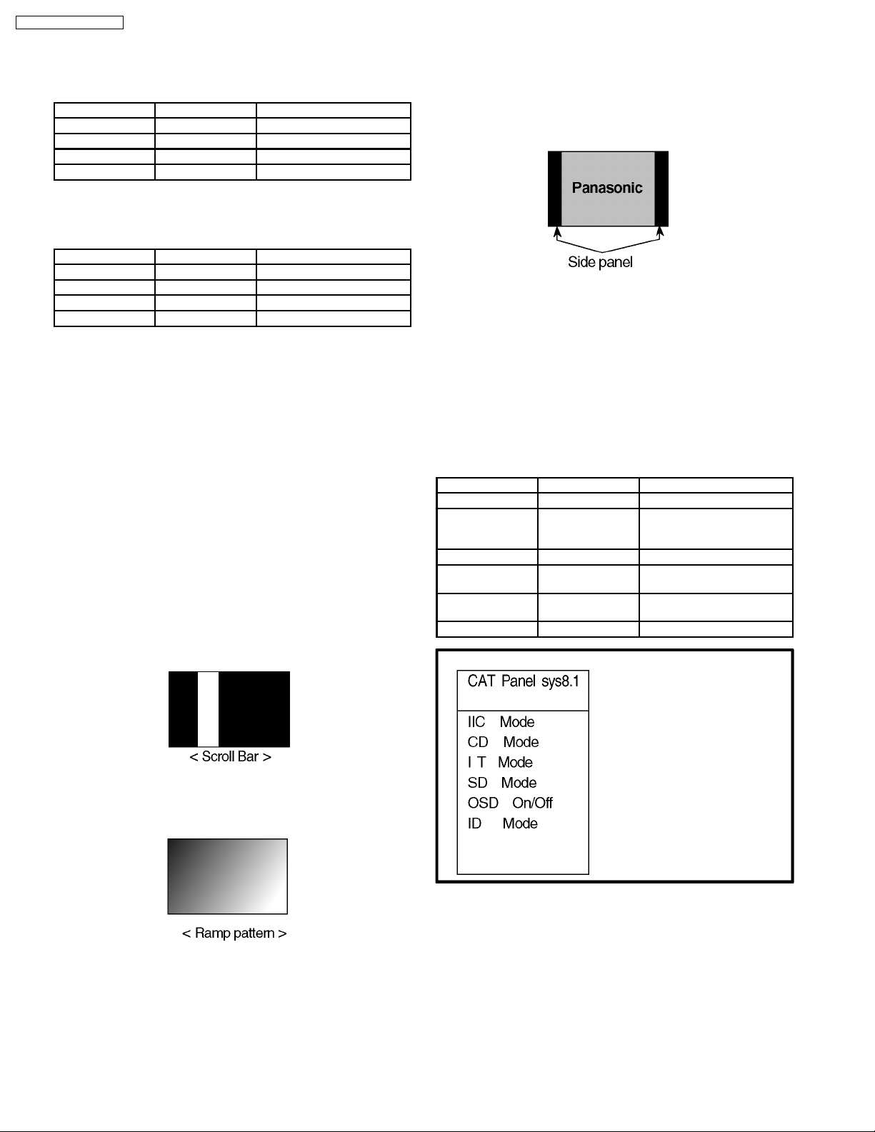
5.13.1. Panel Colour
There are 4 colour pattern White, Red, Blue and Green.
5.13.2. Scroll Bar
Scroll bar is for the after image removal. Display scroll bar
approximately 15 minutes after alignment is competed.
5.14.1. Side panel color setting
Colour of side panel which are left and right side blank area of
4:3 aspect mode can be adjusted as desired color and
brightness.
1. Access Side panel Y(G), U(B) and V(R) by the left or right
button on the remote control.
2. Adjust desired color and brightness of side panel Y(G), U(B)
and V(R) by Volume UP or Down button on the remote
control.
(If 4:3 aspect will be used long time, change side panel
brightness optimum level for screen burn protection.)
5.15. CAT (Computer Aided Test)
mode
Mode Function Access button
IIC Service Alignment Action
CD
(Complete
Diagnostics)
IT (Integrated Text) Not use
SD
(Status Display)
OSD on/off OSD display
ID (Initial Data) Not use
Software version
information EEP
ROM edit
Factory use Action
switch
Mute
Mute
5.13.3. Ramp pattern
Ramp pattern is for digital contrast reproduction confirmation.
5.14. LSI 33 Adjust
LSI 33 PIPCR, LSI 27 Through and ABL Bank are for factory
parameter setting for Format converter (IC9204).
(IT Mode, and ID Mode is unused in serving.)
28
Page 29
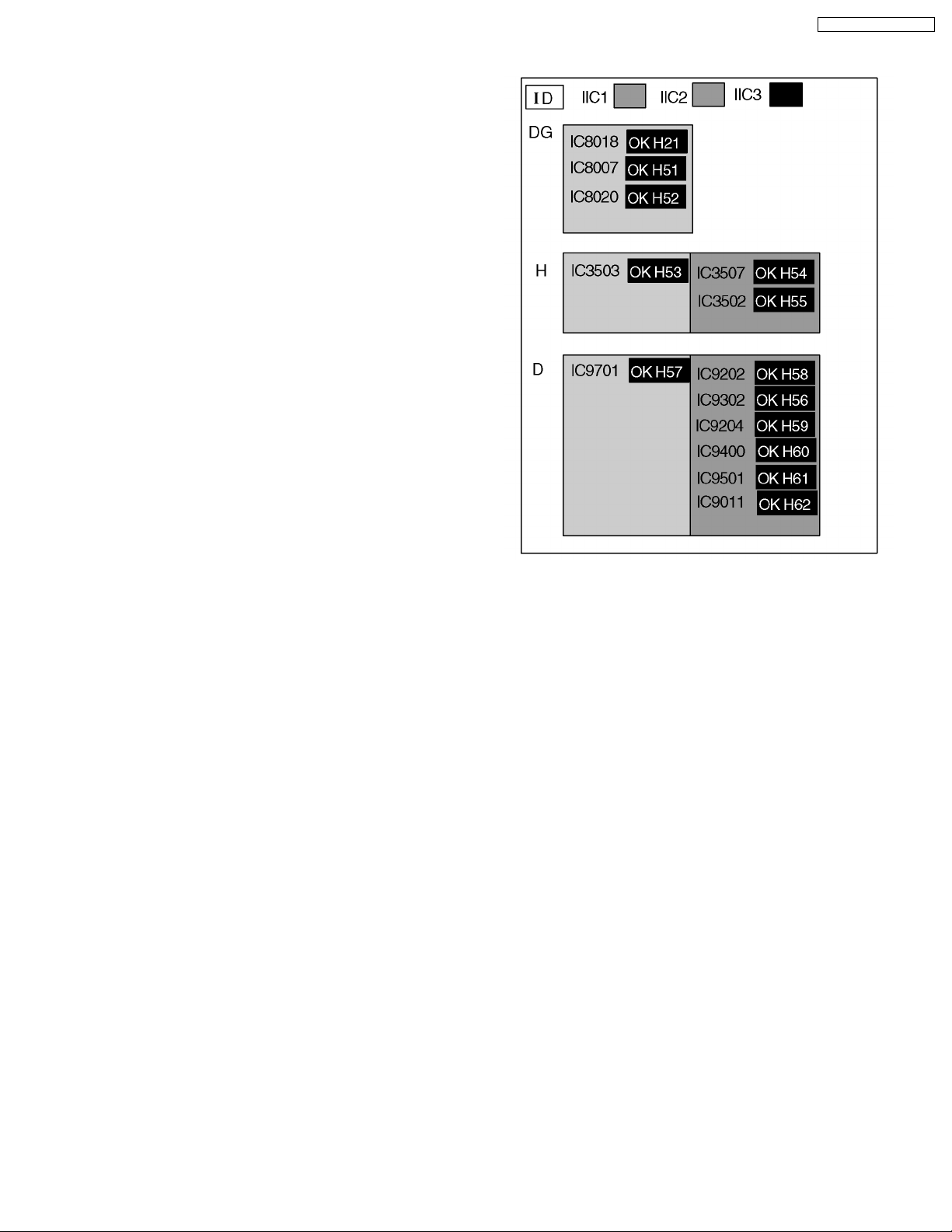
6 Self Check
6.1. Display Indication
1. Self-check is used to automatically check the bus line
controlled circuit of the Plasma display.
2. To get into the Self-check mode press the volume down
button on the customer controls at the front of the set, at the
same time pressing the OFF-TIMER button on the remote
control, and the screen will show :-
If the CCU ports have been checked and found to be incorrect
Or not located then " - - " will appear in place of " OK "
TH-50PHD3 / TH-50PHW3
29
Page 30
TH-50PHD3 / TH-50PHW3
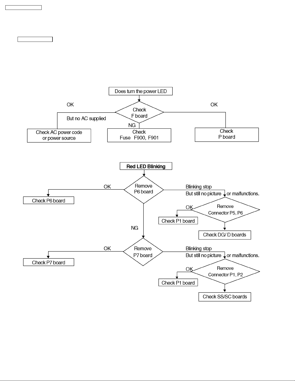
7 Trouble shooting guide
7.1. No Power
First check point
There are following 3 states of No Power indication by power LED.
1. No lit
2. Green is lit then turns red blinking a few seconds later.
3. Only red is lit.
1. No lit
2. Red LED Blinking
When one or some of supply voltages from power supply circuit are declined red LED will be blinking as power
30
Page 31
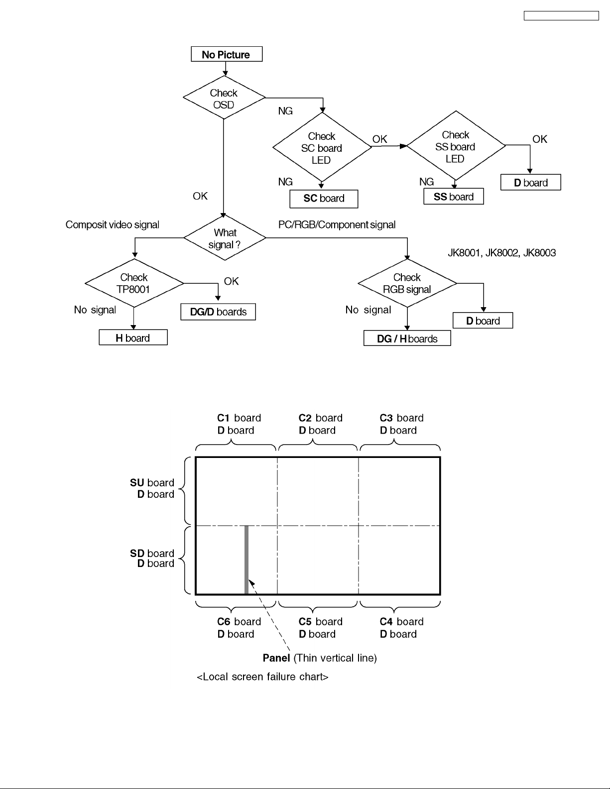
7.2. No Picture
TH-50PHD3 / TH-50PHW3
7.3. Local screen failure
Plasma display may have local area failure on the screen. Fig - 1 is the possible defect P.C.B. for each local area.
Fig - 1
31
Page 32
TH-50PHD3 / TH-50PHW3
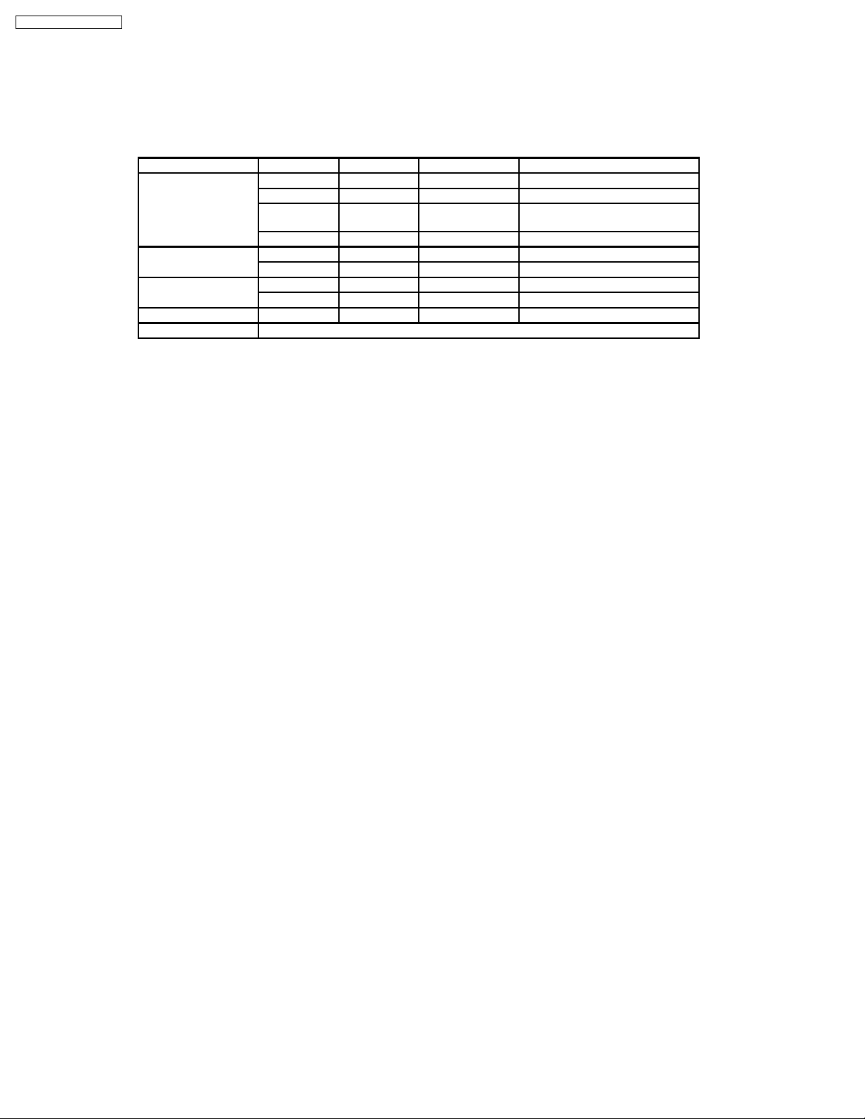
8 P.C.B. (Printed Circuit Board) exchange
8.1. Caution
1. To remove P.C.B. , wait 1 minute after power was off for discharge from electrolysis capacitors.
8.2. Quick adjustment after P.C.B. exchange
P.C.B. Item Volume Test point Level
P board Vsus R639 TPVsus (SS) Vsus ± 1 V
Vbk R513 TPVBK (SC) 140V ± 5 V
Vda R528 P27 connector
pin2
PFC R548 P4 conne ctor pin 1 400V ± 1 V
DG board DG contrast DG contrast TP8004(DG) Refer to the alignment procedure
DVCO DVCO adjust Automatic
SC board Vset R6940 TPSET(SC) 224V ± 1 V
Vad R960 TPVAD VAD ± 1 V
SS board Ve R6829 TPVE VE ± 1 V
D board White balance, Pedestal and Sub brightness for NTSC, PAL, HD, PC and 625I signals.
75V ± 0.5 V
32
Page 33
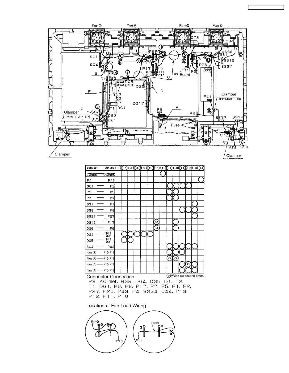
9 Location of Lead Wiring
TH-50PHD3 / TH-50PHW3
33
Page 34
TH-50PHD3 / TH-50PHW3
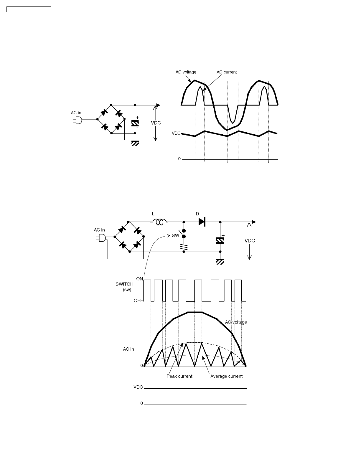
10 Basic Circuit Explanation
10.1. Power Supply Circuit
10.1.1. Power Factor Control (PFC)
10.1.1.1. Basic operation of the Full wave bridge rectifier
Feature:
1. Power Factor 05~0.7
2. Spick AC current with high frequency component.
10.1.1.2. Power Factor control circuit
Feature:
1. Power Factor More than 0.9
2. Automatic Power Factor Control by OFF period change
3. Lower high frequency noise.
34
Page 35
TH-50PHD3 / TH-50PHW3
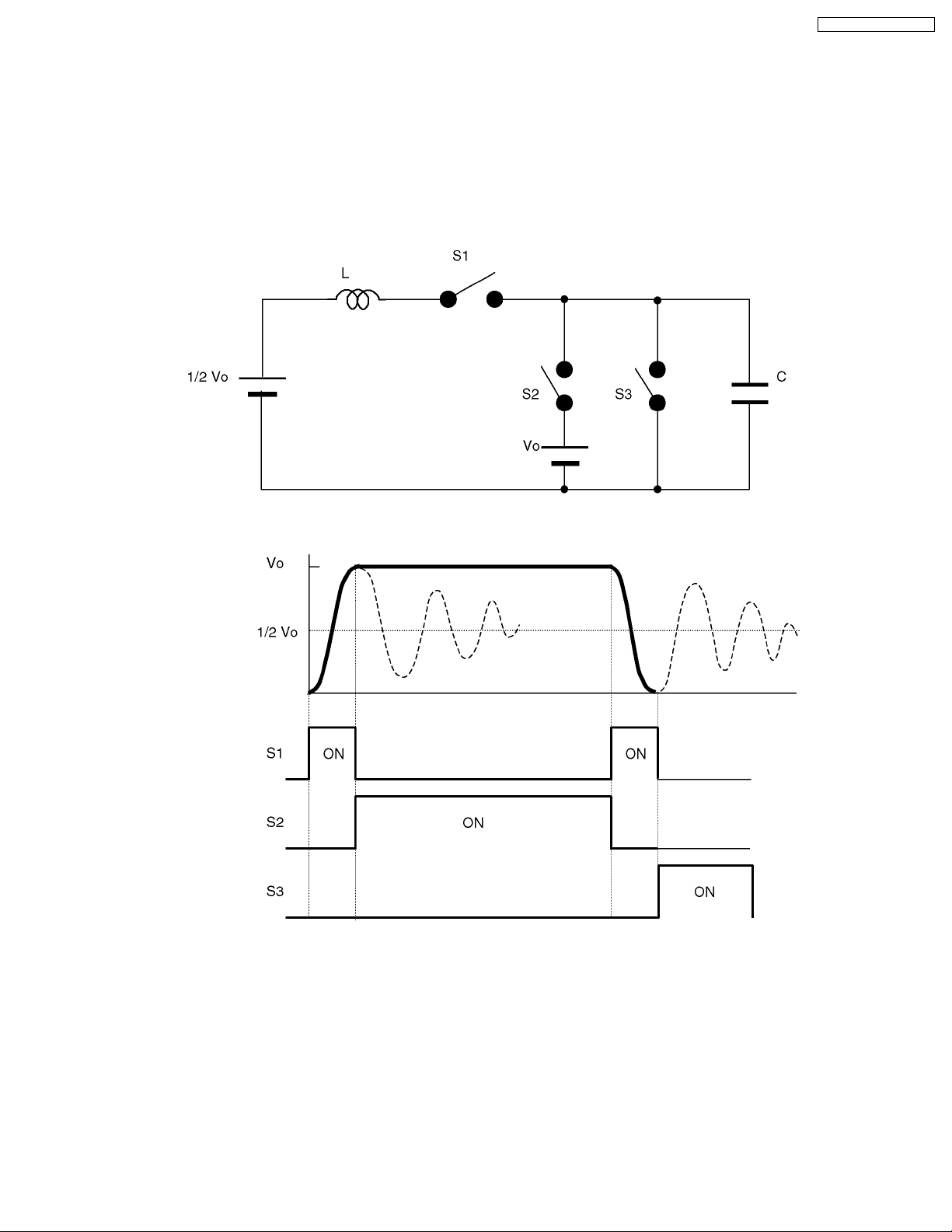
10.2. Energy Recovery Drive Pulse Output
10.2.1. Plasma Panel Energy Loss
When The Sustain, Scan and Data drive pulses are supplied to the plasma panel a lot of energy was lost by resistance of the
electrodes lead and many of switching elements. Because plasma panel has the stray capacitance and this capacitance makes
high level inrush current during the charge and dischange.
This energy loss becomes high temperature from the plasma panel itself.
10.2.2. Energy Recovery circuit
10.2.2.1. Basic operation of the energy recover circuit
35
Page 36
TH-50PHD3 / TH-50PHW3
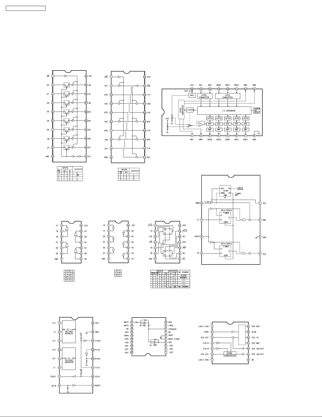
11 IC Block Diagram
C0JBAF000405
TC74LCX574F
(D-TYPE FLIP-FLOP)
C0JBAD000080
(QUAD 2-INPUT
NOR GATE)
C0JBAZ001201
TC74HC244AF
(BUS BUFFER)
C0JBAB000155
C0JBAB000226
(HEX SCHMITT
INVERTER)
CXA1315M
(IIC-DAC CONVERTER)
UC2715N
(FET DRIVER)
TC74LCX74F
C0ZBZ0000205
(RS232C DRIVER)
C1AA00000561
(AMPLIFIER)
36
C0ABFA000012
(HIGH-PERFORMANCE
PHASE-LOCKED LOOP)
Page 37
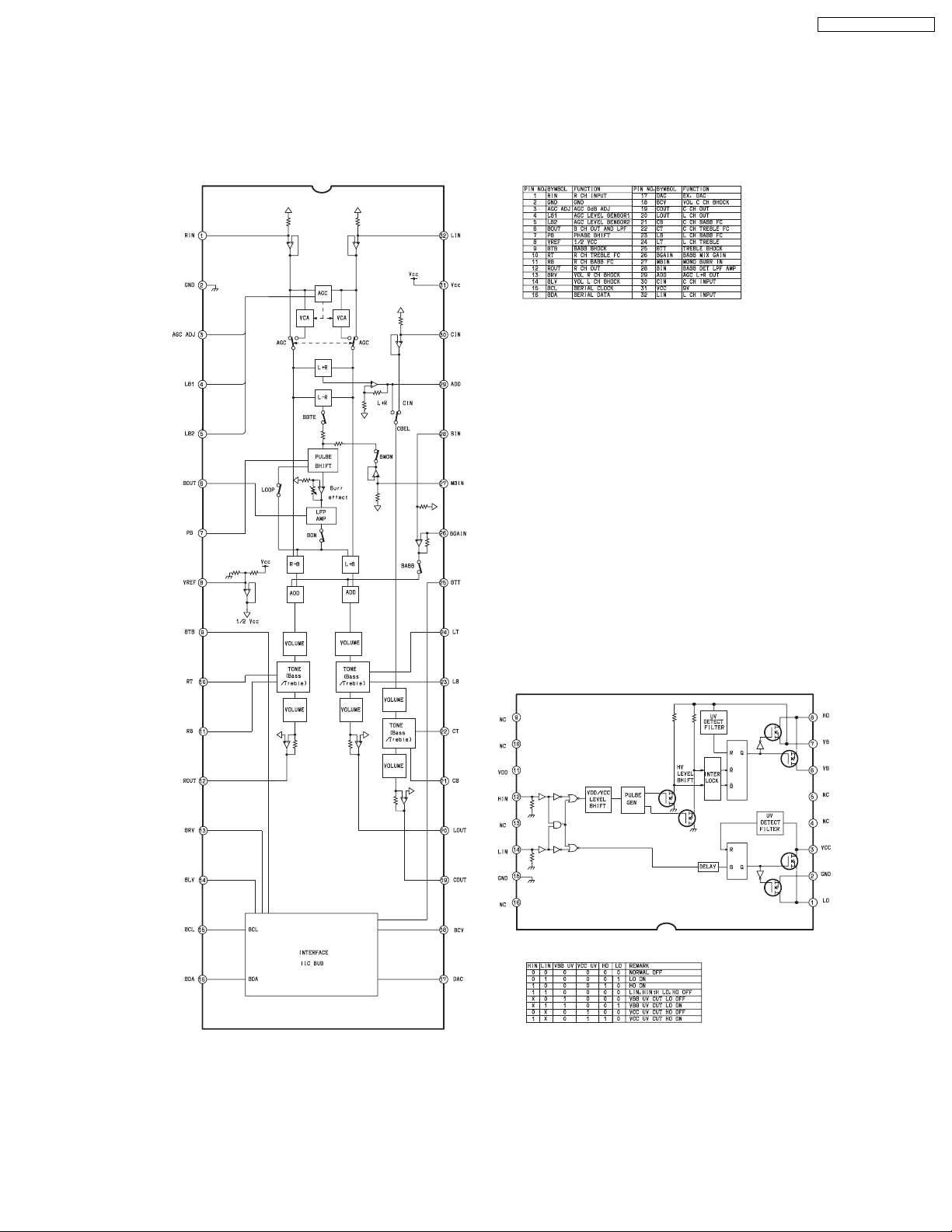
BH3866S
(AUDIO AMP)
TH-50PHD3 / TH-50PHW3
C0ZBZ0000138
(HALF BRIGE DRIVER)
37
Page 38

TH-50PHD3 / TH-50PHW3
38
Page 39
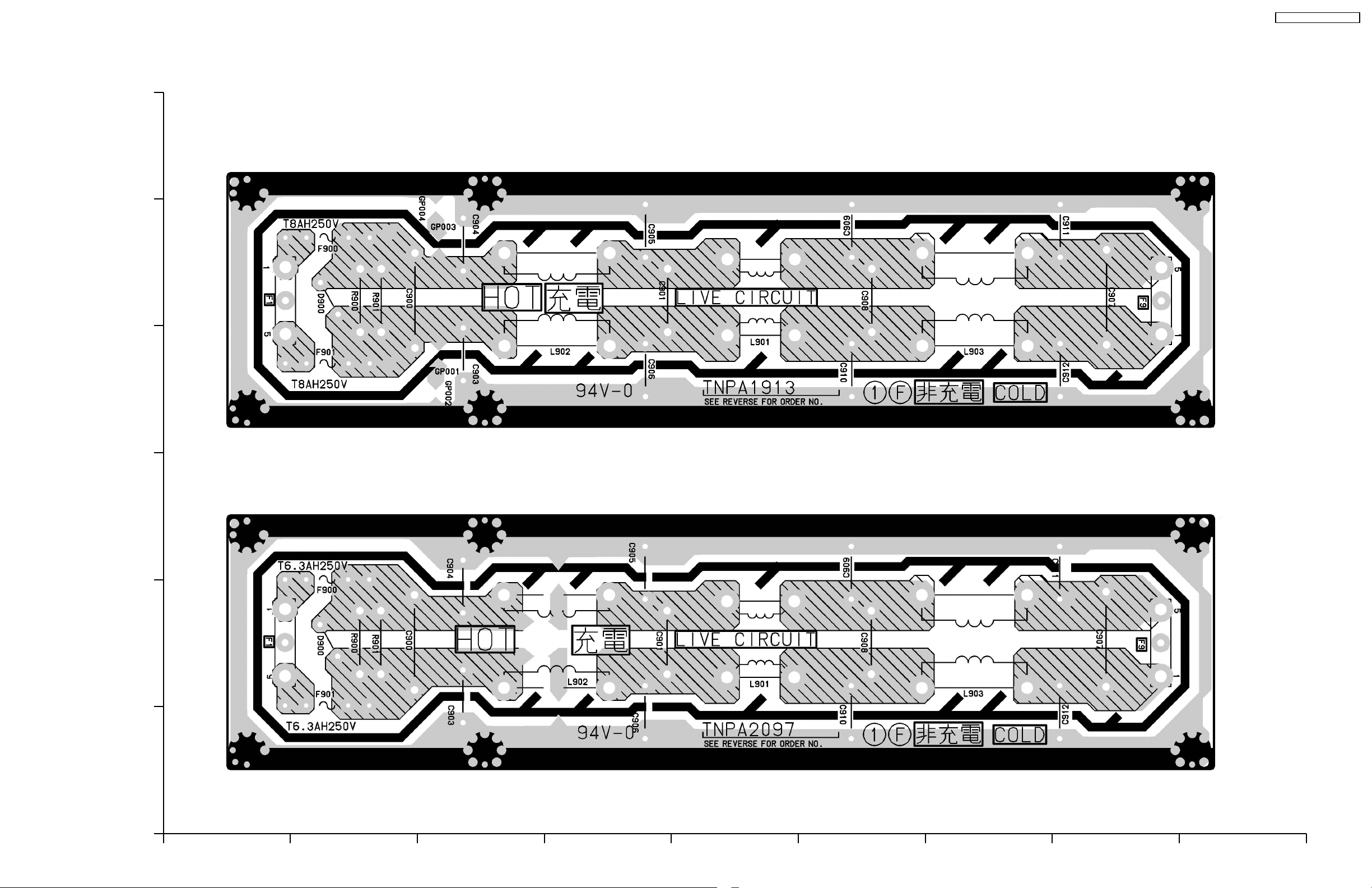
12 Conductor Views
12.1. F-Board
TH-50PHD3 / TH-50PHW3
6
F-BOARD (FOIL SIDE)
TXN/F10L32 (U Version)
5
4
F-BOARD (FOIL SIDE)
TXN/F10HAS (A,B,and E Version)
3
2
1
ABCDEFGH I
39
Page 40
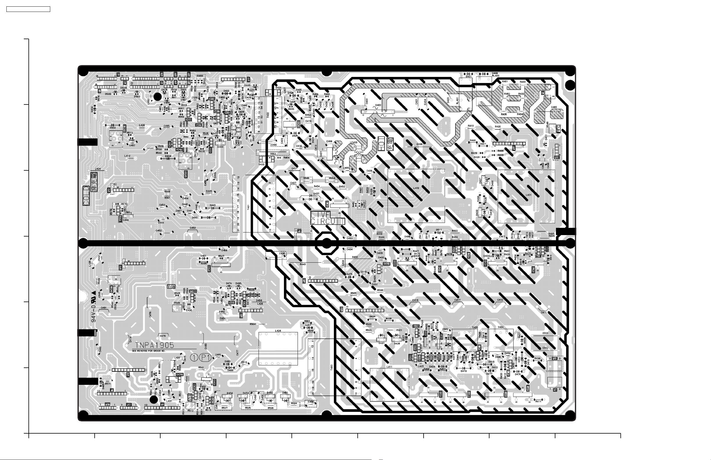
TH-50PHD3 / TH-50PHW3
12.2. P1-Board
6
5
P1-BOARD (FOIL SIDE)
TXNP110L32
4
3
2
1
ABCDEFGH I
40
Page 41
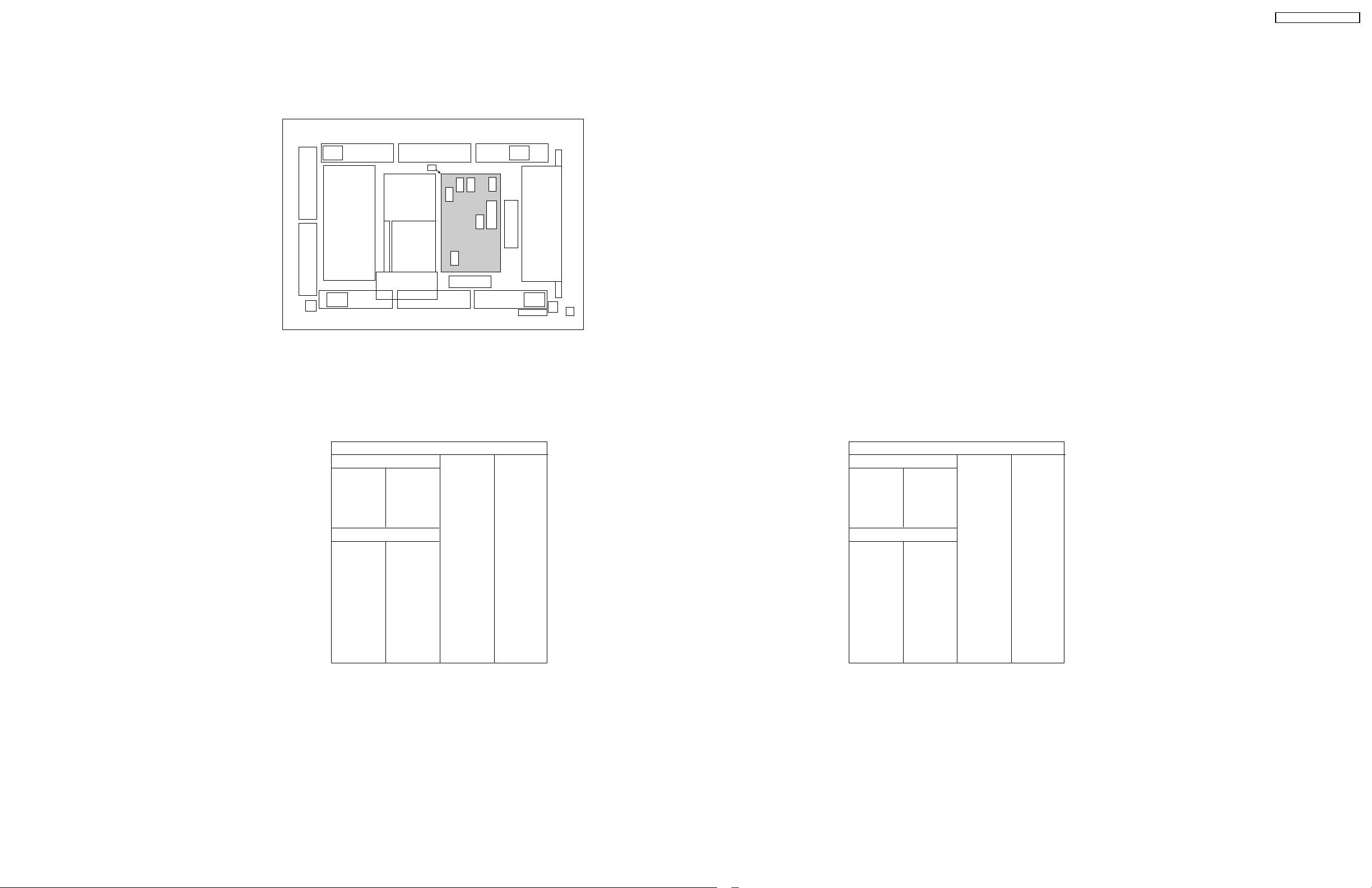
TH-50PHD3 / TH-50PHW3
P1
PARTS LOCATION
P1-BOARD (FOIL SIDE)
IC
IC406 C-3
IC407 B-5
IC410 C-1
IC411 B-3
IC412 C-4
IC421 C-1
TARNSISTOR
Q401 G-3
Q402 G-2
Q403 G-2
Q404 G-3
Q405 H-3
Q406 F-2
Q407 F-2
Q408 F-2
Q409 F-2
Q410 H-1
Q411 G-2
Q412 H-1
Q413 H-1
ADDRESS INFORMATION
Q414 G-1
Q415 G-1
Q416 E-4
Q417 C-5
Q418 C-6
Q419 H-3
Q422 C-5
Q423 F-3
Q424 G-3
Q425 G-3
Q426 C-3
Q427 C-5
Q428 C-5
Q429 C-5
Q430 D-2
Q431 D-2
Q432 C-5
Q434 C-1
Q436 C-1
Q437 B-4
PARTS LOCATION
P1-BOARD (COMPONENT SIDE)
IC
IC406 G-3
IC407 H-5
IC410 G-1
IC411 H-3
IC412 G-5
IC421 G-1
TRANSISTOR
Q400 B-3
Q401 C-3
Q402 C-2
Q403 D-2
Q404 C-3
Q405 B-3
Q406 D-2
Q407 D-2
Q408 D-2
Q409 D-2
Q410 B-2
Q411 C-2
Q412 B-1
ADDRESS INFORMATION
Q413 B-1
Q414 D-1
Q415 C-1
Q416 D-4
Q417 G-5
Q418 B-3
Q418 G-6
Q421 G-5
Q422 G-5
Q423 D-3
Q424 C-3
Q425 C-3
Q426 G-3
Q427 G-5
Q428 G-5
Q429 G-5
Q430 F-3
Q431 F-3
Q432 G-5
Q434 G-1
Q436 G-1
Q437 H-4
41
Page 42
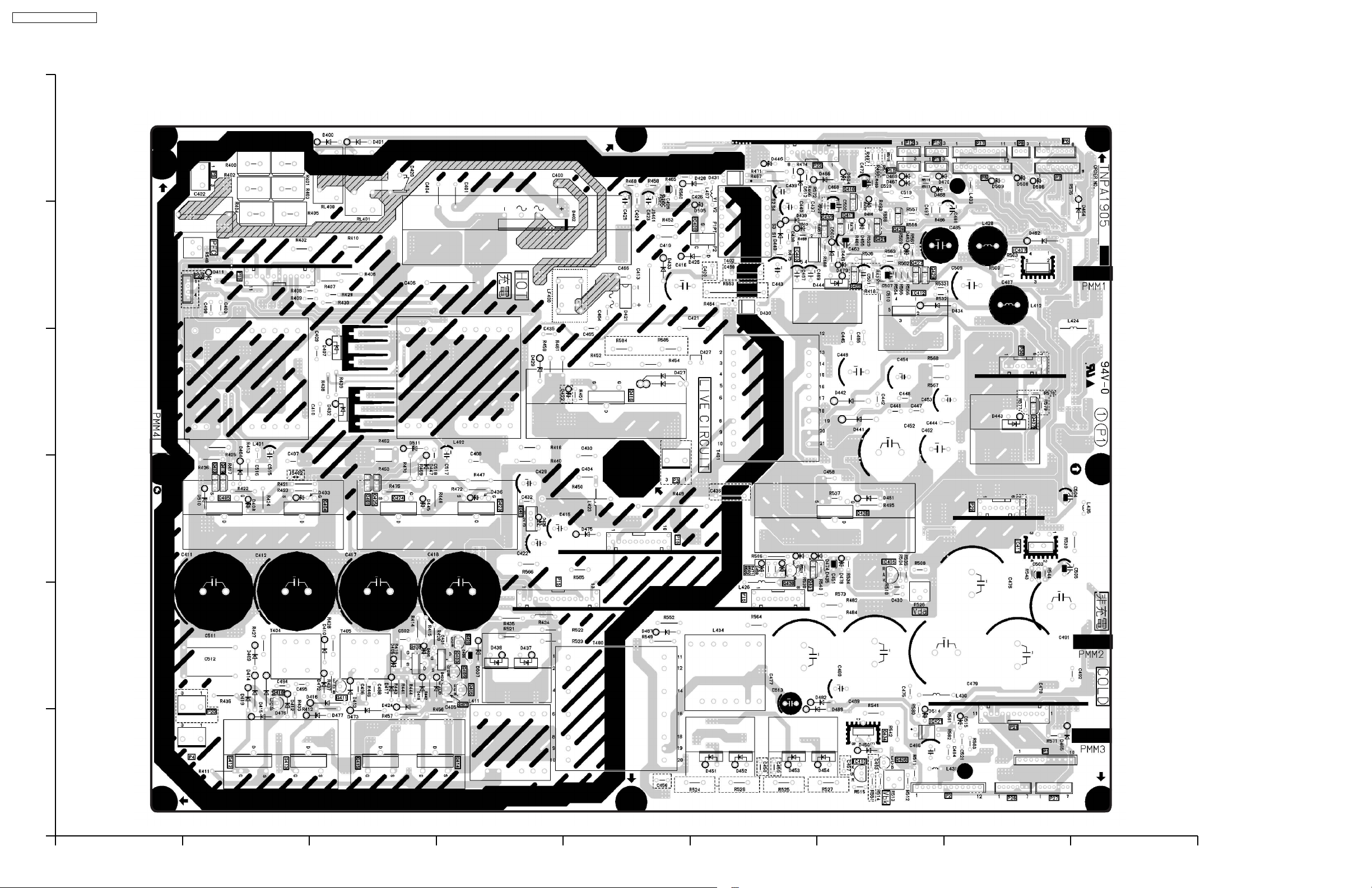
TH-50PHD3 / TH-50PHW3
6
5
P1-BOARD (COMPONENT SIDE)
TXNP110L32
4
3
2
1
ABCDEFGH I
42
Page 43
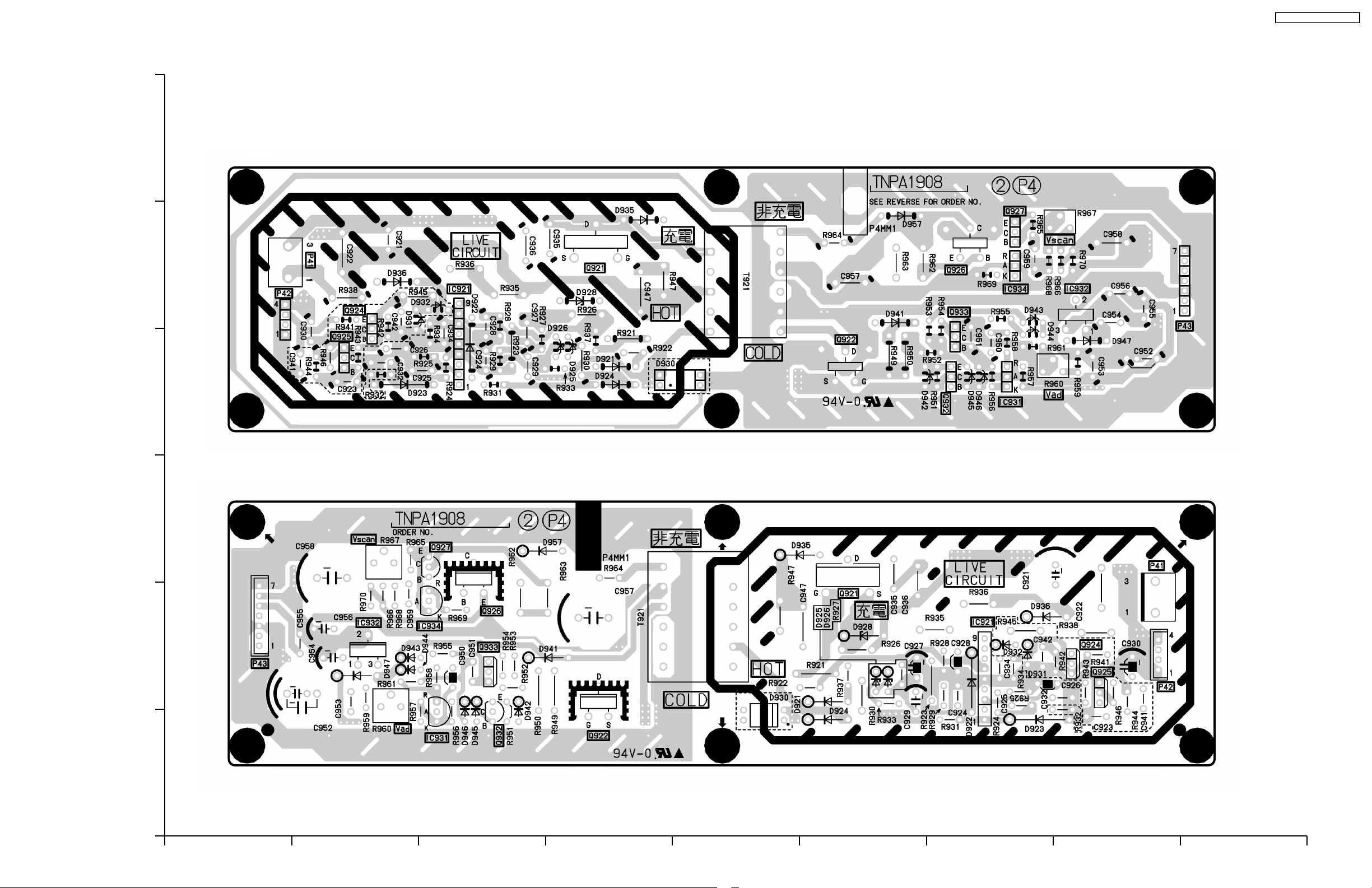
12.3. P4-Board
TH-50PHD3 / TH-50PHW3
6
P4-BOARD (FOIL SIDE)
TNPA1908
5
4
P4-BOARD (COMPONENT SIDE)
TNPA1908
3
2
1
ABCDEFGH I
43
Page 44
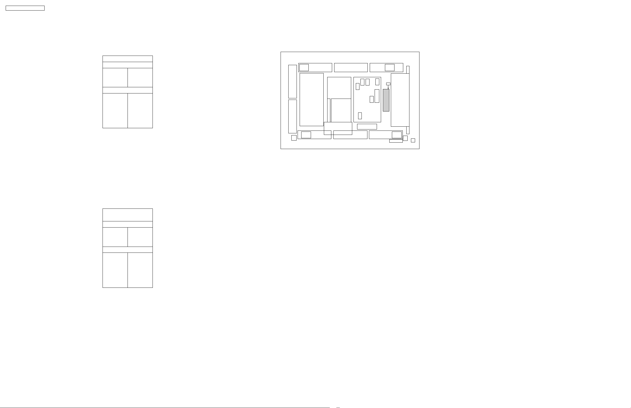
TH-50PHD3 / TH-50PHW3
PARTS LOCATION
P4-BOARD (FOIL SIDE)
IC
IC921 C-4
IC931 G-4
IC932 H-5
IC934 G-5
TRNSISTOR
Q921 D-5
Q922 F-4
Q924 B-5
Q925 B-4
Q926 G-5
Q927 G-5
Q932 G-4
Q933 G-5
ADDRESS INFORMATION
P4
PARTS LOCATION
P4-BOARD
(COMPONENT SIDE)
IC
IC921 G-2
IC931 C-1
IC932 B-2
IC934 C-2
TRANSISTOR
Q921 F-2
Q922 D-1
Q924 H-2
Q925 H-2
Q926 C-2
Q927 C-3
Q932 C-1
Q933 C-2
ADDRESS INFORMATION
44
Page 45
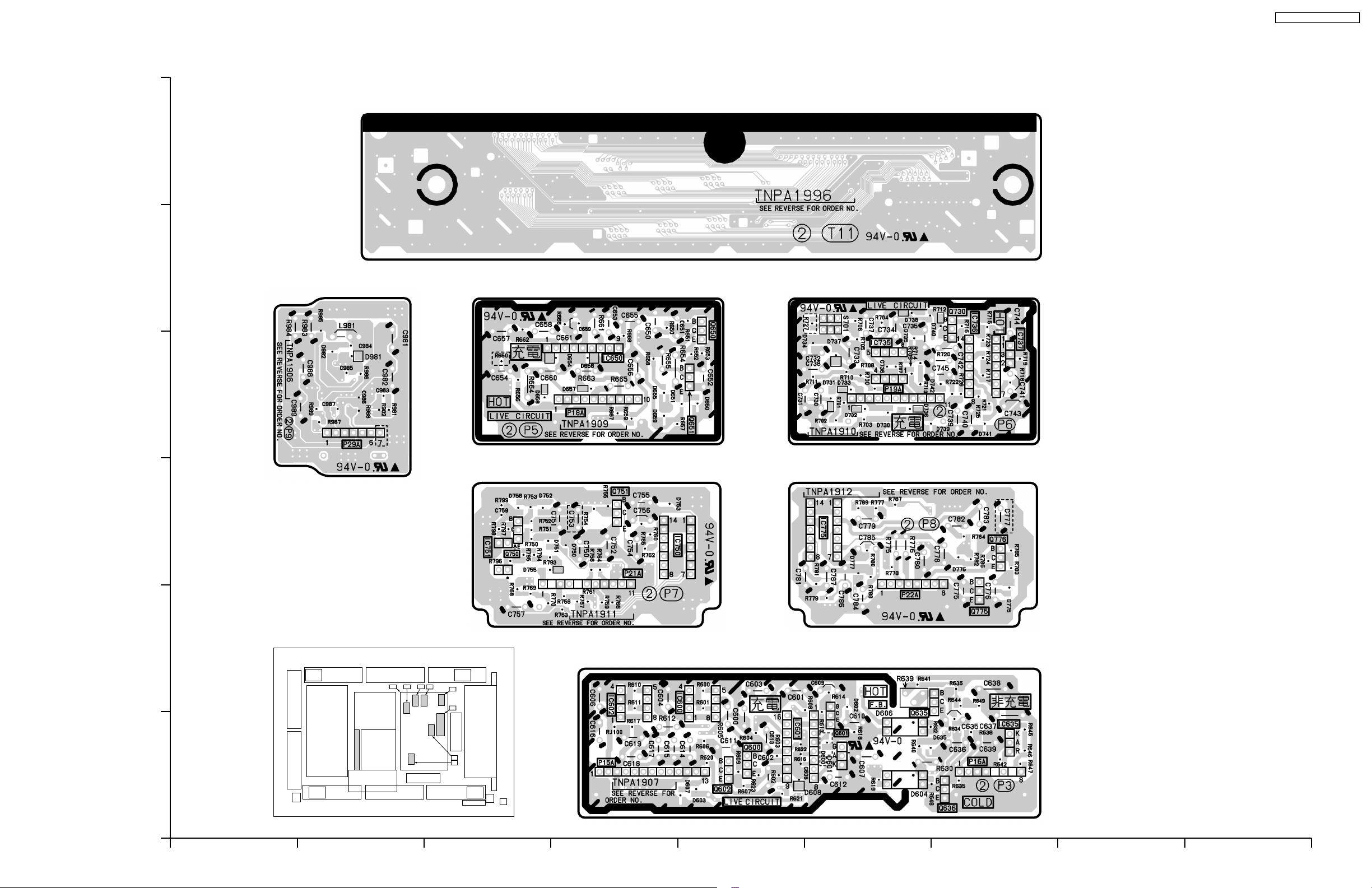
12.4. P3, P5, P6, P7, P8, P9 and T11-Board
T11-BOARD (FOIL SIDE)
TNPA1996
6
TH-50PHD3 / TH-50PHW3
5
P9-BOARD (FOIL SIDE)
TNPA1906
P5-BOARD (FOIL SIDE)
TNPA1909
P6-BOARD (FOIL SIDE)
TNPA1910
4
P7-BOARD (FOIL SIDE)
TNPA1911
P8-BOARD (FOIL SIDE)
TNPA1912
3
2
P3-BOARD (FOIL SIDE)
TNPA1907
P1 P8
P9 P9
P7
P3
P5
P6
1
ABCDEFGH I
45
Page 46
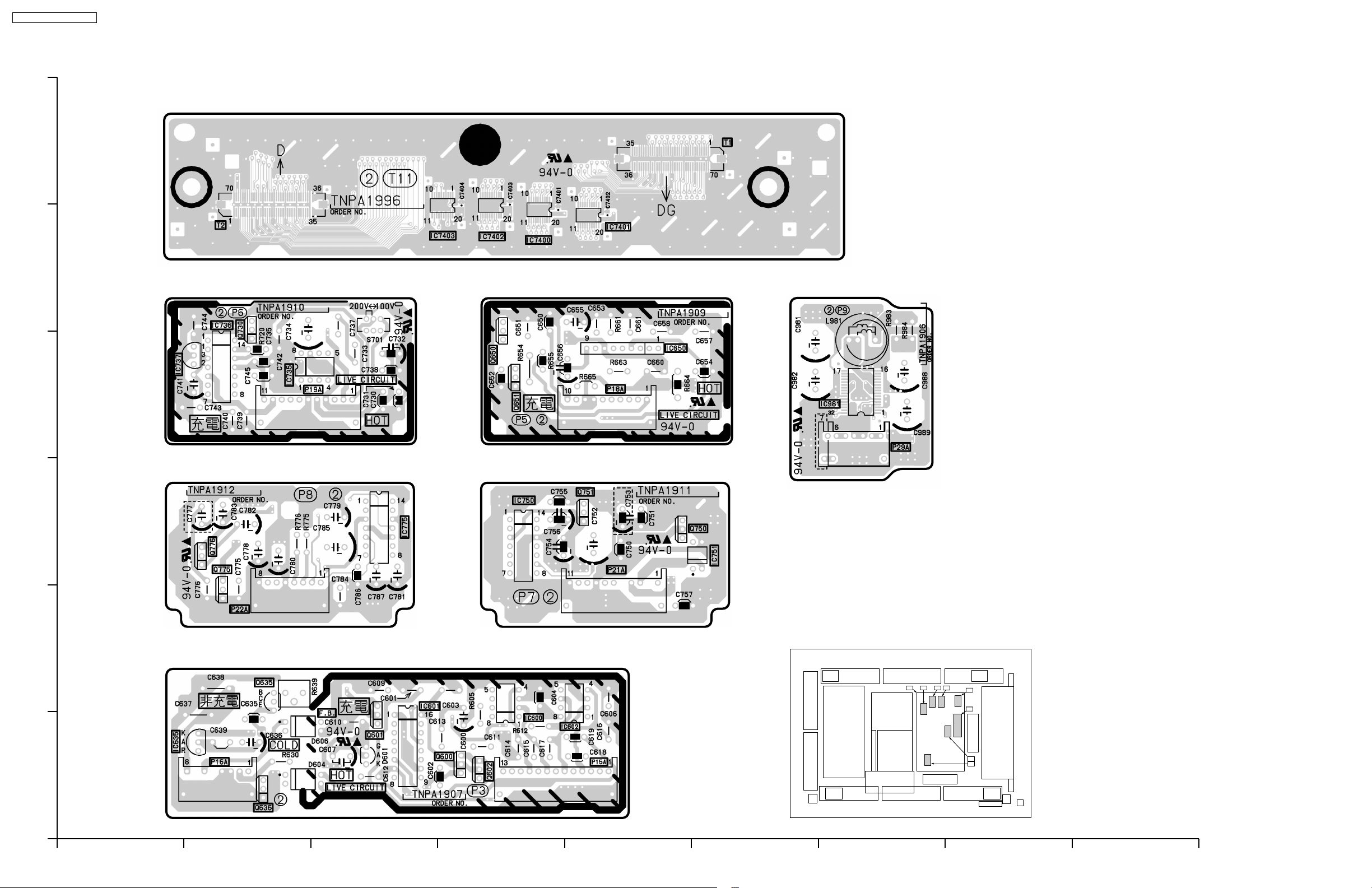
TH-50PHD3 / TH-50PHW3
6
T11-BOARD (COMPONENT SIDE)
TNPA1996
5
P6-BOARD (COMPONENT SIDE)
TNPA1910
P5-BOARD (COMPONENT SIDE)
TNPA1909
P9-BOARD (COMPONENT SIDE)
TNPA1906
4
P8-BOARD (COMPONENT SIDE)
TNPA1912
P7-BOARD (COMPONENT SIDE)
TNPA1911
3
2
P3-BOARD (COMPONENT SIDE)
TNPA1907
P1 P8
P9 P9
P7
P3
P5
P6
1
ABCDEFGH I
46
Page 47
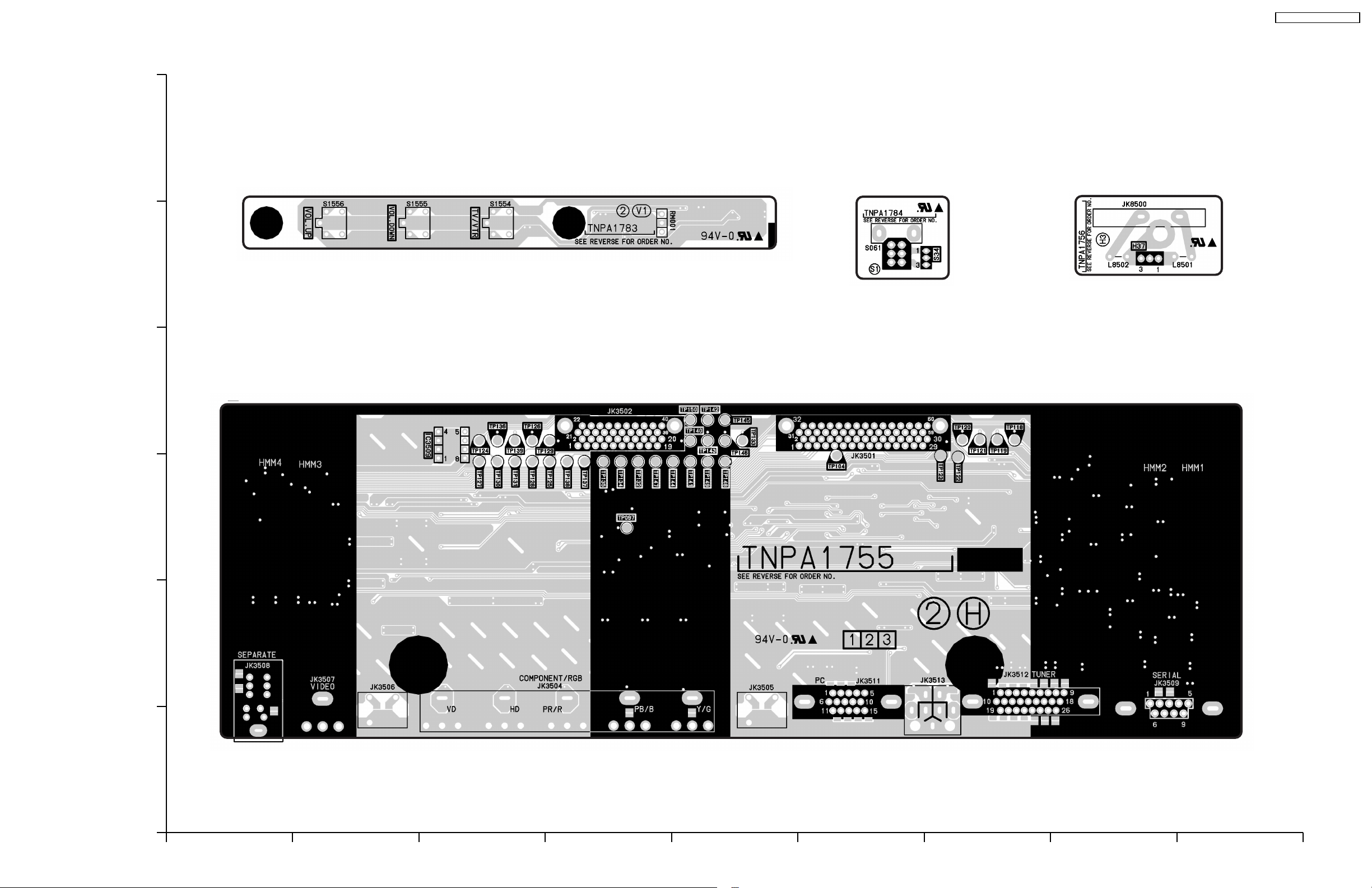
12.5. H, H3, S1 and V1-Board
6
TH-50PHD3 / TH-50PHW3
V1-BOARD (FOIL SIDE)
TNPA1783
5
S1-BOARD
TNPA1784
H3-BOARD
TNPA1756AB
H-BOARD (FOIL SIDE)
4
TNPA1755
3
2
1
ABCDEFGH I
47
Page 48
TH-50PHD3 / TH-50PHW3
H
PARTS LOCATION
H-BOARD (FOIL SIDE)
IC
IC3509 C-4
TEST POINT
TP097 D-3
TP104 F-3
TP118 G-4
TP119 G-4
TP120 G-4
TP121 G-4
TP122 G-3
TP123 G-3
TP124 C-4
TP125 D-3
TP126 C-4
TP127 C-3
TP128 C-3
TP129 C-4
TP130 C-3
TP131 C-3
TP132 D-3
TP133 E-4
ADDRESS INFORMATION
TP134 D-3
TP135 D-3
TP136 C-4
TP137 D-3
TP138 D-3
TP139 C-4
TP140 E-4
TP141 E-3
TP142 E-4
TP143 E-4
TP144 D-3
TP145 E-4
TP146 E-4
TP147 D-3
TP148 E-3
TP149 E-3
TP150 E-4
PARTS LOCATION
H-BOARD (COMPONENT SIDE)
IC
IC3502 D-2
IC3503 B-3
IC3504 E-3
IC3505 E-3
IC3506 H-3
IC3507 F-3
IC3508 D-3
IC3509 G-4
IC3510 I-3
IC3511 B-2
IC3513 B-3
IC3514 C-3
IC3515 B-2
TRNSISTOR
Q3501 I-3
Q3502 I-3
Q3503 H-3
Q3504 E-2
Q3505 F-2
Q3506 F-2
Q3507 D-2
Q3508 D-2
Q3509 D-2
ADDRESS INFORMATION
Q3510 C-2
Q3511 C-2
Q3512 C-2
Q3513 E-2
Q3514 E-2
Q3515 E-2
Q3517 G-2
Q3518 G-2
Q3519 G-2
Q3520 G-2
Q3521 C-2
Q3522 C-2
Q3523 C-2
Q3524 B-2
Q3525 H-3
Q3526 G-3
Q3527 H-2
Q3528 H-2
Q3529 H-3
Q3530 G-3
Q3531 H-3
Q3532 H-2
Q3533 G-3
Q3534 H-3
Q3535 B-3
Q3536 C-3
48
Page 49
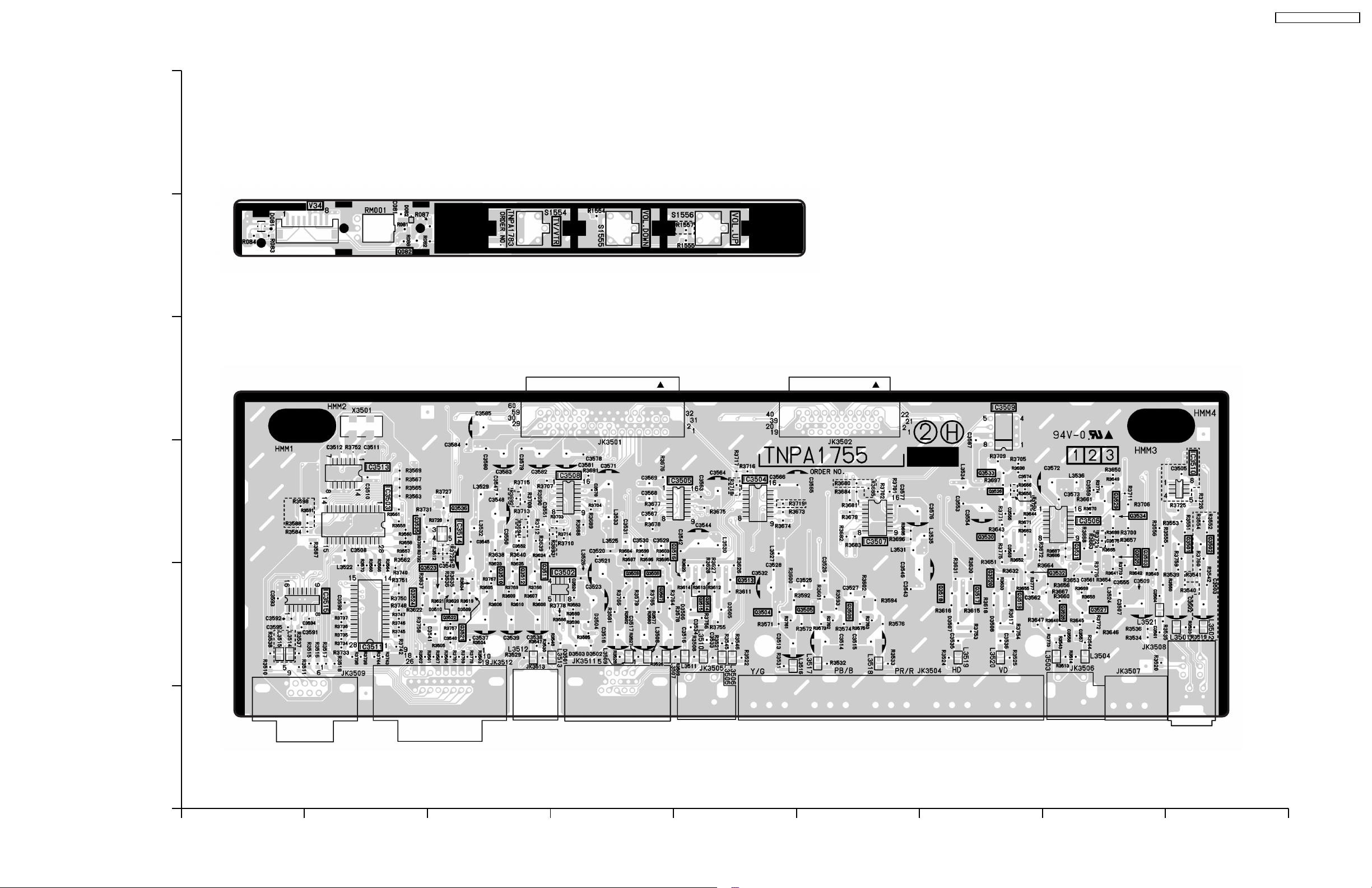
TH-50PHD3 / TH-50PHW3
6
V1-BOARD (COMPONENT SIDE)
TNPA1783
5
H-BOARD (COMPONENT SIDE)
4
3
2
TNPA1755
1
ABCDEFGH I
49
Page 50
TH-50PHD3 / TH-50PHW3
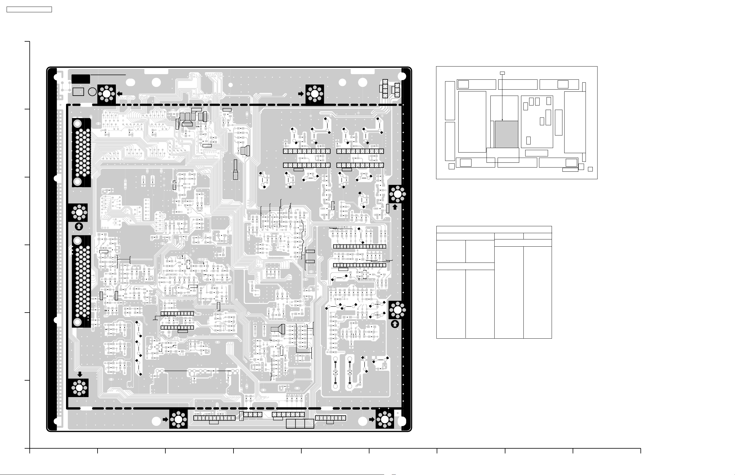
12.6. DG-Board
DG-BOARD (FOIL SIDE)
TXNDG10L33
6
DG
SEE REVERSE FOR ORDER NO.
TNPA1754
3
4
DG4
1
3
DG5
1
DG
TP8017
C8162
TP8014
C8060
R8095
R8088
R8084
R8083
R8042
R8147
JS8004
C8059
C8050
R8085
C8081
R8244
Q8022
R8071
C8074
C8030
R8082
C8098
C8094
R8093
C8064
C8053
C8054
R8140
R8130
R8086
IC8010
C8011
R8080
R8120
TP8016
R8278
C8082
R8098
R8063
21
22
5
39
40
1
2
JK8502
19
20
C8160
JS8024
C8158
C8087
C8156
C8086
4
C8185
R8040
31
32
3
59
60
2
1
2
R8005
R8006
R8002
JK8501
C8001
29
30
C8027
R8035
R8050
C8004
Q8005
C8002
C8003
R8017
R8019
Q8001
R8252
R8021
R8015
R8029
R8053
R8011
R8007
R8008
R8009
R8010
R8038
R8249
R8012
R8033
R8054
Q8006
C8017
C8163
R8020
R8016
R8018
R8048
R8069
C8033
R8075
R8251
R8025
R8026R8027
C8036
JS8019
R8432
R8046
R8013
R8023
R8074
R8066
R8034
C8022 C8023C8024
R8068
R8078
R8065
C8178
R8250
R8089
R8081
C8041
Q8014
C8034
JS8001
R8072
C8047
R8091
R8090
C8172
R8145
C8080
C8065
C8057
R8430
R8087
R8062
R8136
11
10
R8092
Q8021
C8079
C8100
Q8020
Q8012
C8068
R8137
C8184
R8067
R8058
R8070
20
1
R8114
R8101
C8176
R8131
R8429
C8101
R8103
JS8002
C8168
TP8015
R8435
R8434
Q8033
R8132
JS8003
R8332
C8026
R8052
R8032
C8015
R8431
C8012
C8072
R8100
R8079
R8613
C8014
R8047
R8612
C8170
R8282
R8134
C8044
C8025
Q8003
R8133
C8046
R8028
R8245
R8185
Q8030
R8030
R8024
R8043
R8182
C8048
C8167
R8036
R8617
R8124
R8044
JS8023
TP8013
R8615
R8127
JS8021
R8280R8281
JS8022
R8614
R8192
C8303
TP8018
R8333
R8334
R8191
R8193
R8311
R8184
R8247
C8136
C8128
R8176
C8124
R8173
C8105
R8335
R8248
C2344
R8306
C8304
R8313
R8317
C8130
C8149
C8126
R8160
C8116
C8119
C8134
R8181
R8187
C2340
R8327
C8151
C8305
R8315
R8319
C8308
C8148
C8138
C8131
C8133
R8156
R8194
R8174
C8309
C2316
R2322 R2323
C2318 C2319
C2320 C2321
C2328 C2329
IC2301
C2322
C2341
C2323
C2338
R2335
C2349
R2321
R8304
R8305
R2319
C8302
R8303
Q8050
R8301
R8328
R8323
Q8049
R8321
R8320
C8140
C8153
R8189
R8190
C8139
R8228
R8227
R8226
R8225
R8222
R8221
R8205
R8201
R8198
R8197
R8196
C8110
C8107
R8179
R8180
R8427
C8150
Q8032
R8310
R8307
R8316
R8322
R8325
C8109
TP8004
C8127
R8177
20
C2345
C8142
C8135
C2326
R8183
R8326
R8324
L2301
R8309
R8308
R8178
C2330
L2303
C2337
R2330
R2426
R2447
R2326
C2331
1110120
R2460
C2412
C2409
R2434
C2426
C2432
R2449
R2448
R2466
D2306
Q2301
R2467
C2411
R2423
JS2302
C2327
R2468
R2463
1
C2433
32
R2417
C2437
R2431
C2347
R2419
1
R2317
C2315
R2318
IC2401
R2441
C2452
L2302
IC2302
R2418
C2415
R2452
C2414
R2442
D2305
R2453
C2434
JS2303
C2343
R2304
R2416
R2444
C2428
R2454
C2453
C2408
R2446
R2347
R2428
R2436
R2301
C2455
C2436
R2346
JS3
JS2301
C2346
R2456
C2324
C2325
JS8
R2435
C2317
R2308
JS2
C2313
Q2306
R2433
R2427
R2405
C2342
R2307
C2461
JS7
C2418
C2332
C2463
R2432
C2339
R2430
R2429
R2331
R2348
L2304
R2336
D2308
R2425
C2431
C2314
C2312
R2327
C2333
C2350
R2476
1110
C2402
C2429
C2464
R2305
R2324
C2336
R2329
17
Q2302
R2477
16
C2458
C2460
R2333
C2462
PARTS LOCATION
DG-BOARD (FOIL SIDE)
IC
IC2301 D-5
IC2302 E-5
IC2401 E-3
IC8010 C-2
TRANSISTOR
Q2301 E-4
Q2306 E-3
Q8001 B-3
Q8003 C-3
Q8005 B-3
Q8006 B-3
Q8012 C-3
Q8020 C-3
Q8022 C-4
Q8023 C-5
Q8026 B-2
Q8030 C-5
Q8032 D-2
Q8049 E-3
ADDRESS INFORMATION
Q8050 E-3
TEST PONIT
TP8004 D-2
TP8013 D-5
TP8014 C-5
TP8015 C-5
TP8016 C-5
TP8018 D-5
1
DG98
14
ZIG
1
IIC
DG99
7
123
DG6
18
1
C8173
11
DG17
C8164
C8165
ABCDEFGH I
50
Page 51
TH-50PHD3 / TH-50PHW3
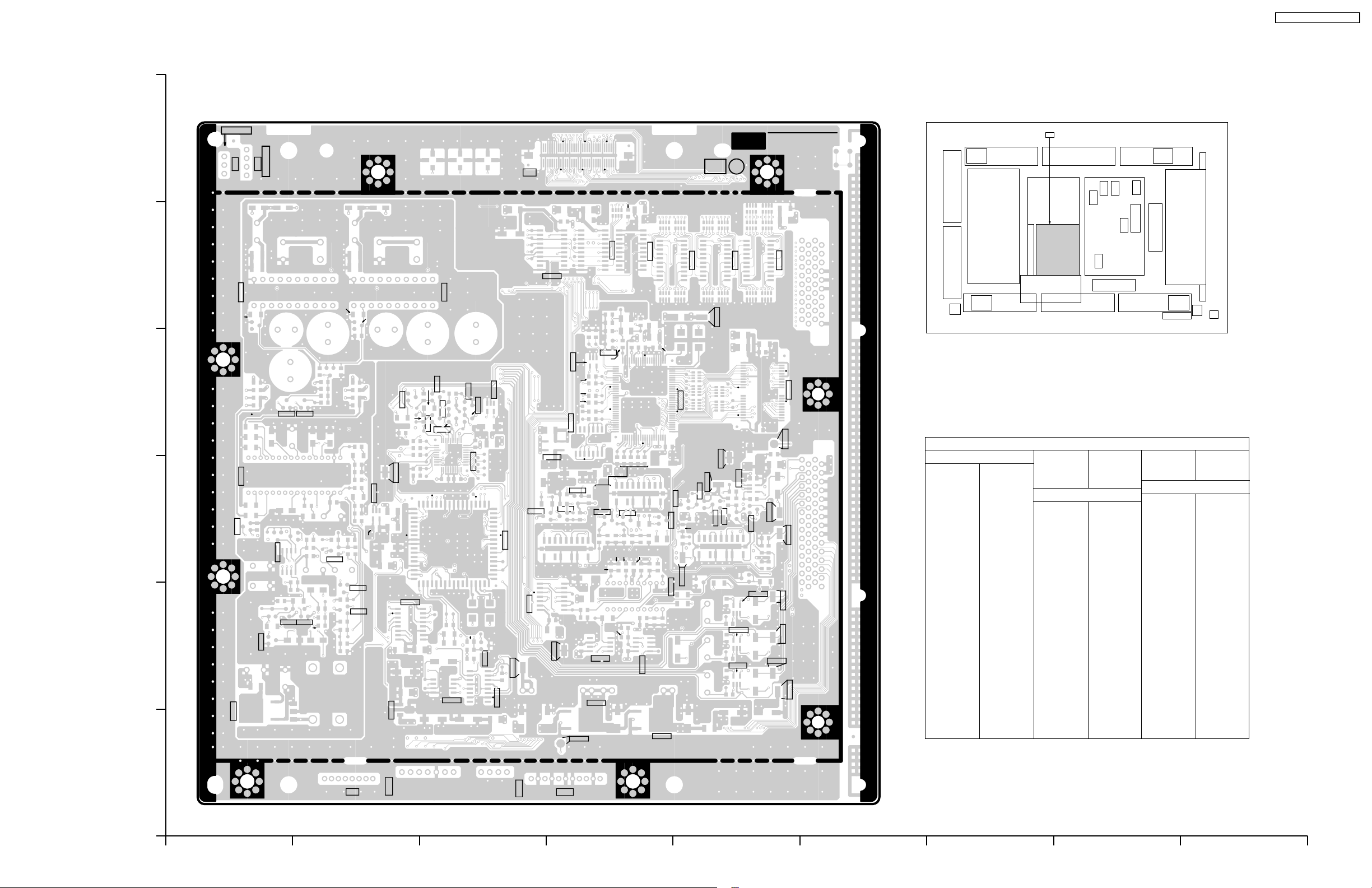
DG-BOARD (COMPONENT SIDE)
TXNDG10L33
6
DG4
DG5
SP LOUT
D2301
D2302D2303 D2304
C2454
IC2402
C2457
R2 424
D2403D2404
C2421
L2305
C2325
C2317
Q2303Q2304
Q2401Q2402
R2445
R2469
C2313
C2455
R2411
R2412
C2413
C2401
C2459
C2420
C2451
C2414
C2427
L2302
R2334
R2443
D2307
C2437
C2410
C2435
Q2403
D2305
R2309
R2310
R2345
R2332
C2419
R2440
C2430
C2450
L2303
C2334
C2348
R2473
R2421
C2389
C2388
R2408
R2471
R2462
R2472
Q2404
R2422
C2423
R2439
R2450
C2347
R2461
C2440
C2456
R2470
C2465
Q2406
R2328
R2320
D2306
R2420
JS6
R2342
R2341
C2409
D2314
C2441
R8200
C8152
IC8019
L8025
L8026
C2323
C8146
IC8021
C2316
C8301
R8302
L2304
C2391
5
4
3
2
R2325
R2344
R2343
IC2304
Q2305
IC2302
C2335
C2422
C2466
C2467
IC2401
C2314
D2315
R2410
L2306
C2390
C2402
C2429
C2474
C2417
R2306
Q2405
C2346
D2405
R2437
C2416
R8329
R8330
TP8012
C8111
L8009
Q8042
L8024
IC8020
R8331
JS8101
R8318
L8023
JS8102
R8312
C8108
B
C8306
Q8048
Q8047
C8114
Q8043
L2301
IC2301
C2345
R8314
Q8045
C8311C8312
R8188
C8132
IC8015
G
C8177
C8106
C8129
R8186
R8175
Q8044
C8310
X8003
JK8001JK8002JK8003
IC8032
Q8046
L8201
Q8031
L8018
R
DG
3
DG1
R8276
R8113
R8112
C8180
Q8013
TP8008
TP8010
R8039
C8021
Q8010
C8018
C8020
C8019
IC8002
IC8003
R8057
R8234
IC8025
R8240
L8015
L8016
C8032
R8041
R8037
C8038
D8017
IC8001
R8061
R8277
R8236
R8242
C 8016
C8084
C8063
IC8004
C8008
Q8007
R8022
C8009
C8049
R8004
C8179
R8014
L8001
C8037
TS8001
TP8003
C8010
R8001R8003
C8005
C8155
R8235
R8243
L8029
IC8027
JK8502
IC8008
TP8001
C8007
JK8501
TP8002
TS8003
TS8002
TP8005
C8175
IC8031
C2344
IC8014
L8022
C8141
C8307
IC8018
C8103
C8174
TP8009
Q8002
IC8011
C8061
C8095
C8013
L8017
C8166
C8137
IC8016
L8008
IC8006
R8049
TP8011
R8245
L8019
R8045
Q8004
LC8001
R8129
R8125
R8121
D8005
IC8017
C8006
Q8008
R8031
TP8006
IC8012
C8093
L8011
R8123
L8020
C8300
C8075
JS8005
R8426
R8118
R8104
R8051
IC8030
L8002
R8141
IC8009
Q8009
R8055
C8052
C8089
JS8006
Q8023
C8055
R8139
R8094
R8135
R8146
R8056
C8096
C8056
R8237
C8083
C8058
C8169
IC8033
C8051
R8064
C8071
C8070
R8428
L8013
LC8003
Q8016
C8031
R8142
C8045
R8244
C8090
R8073
C8161
L8012
C8091
C8035
C8092
R8117
C8073
C8039
C8099
C8088
L8010
R8077
IC8005
R8143
L8028
IC8028
L8027
R8144
IC8029
R8231
R8239
C8085
R8126
R8138
C8078
C8042
Q8019
IC8010
L8014
C8076
C8077
C8067
Q8018
C8040
X8001
IC8007
C8062
TS8004
R8232
R8238
R8128
R8116
IC8023
C8043
C8024
C8023
R8233
R8241
Q8015
C8022
C8029
LC8002
C8171
L8003
R8122
TP8007
D8016
SP ROUT
TNPA1754
DG
PARTS LOCATION
DG-BOARD (COMPONENT SIDE)
IC
IC2301 C-5
IC2302 A-5
IC2304 A-1
IC2401 A-3
IC2402 A-3
IC8001 E-3
IC8002 E-2
IC8003 E-2
IC8004 E-2
IC8005 D-2
IC8006 D-3
IC8007 E-4
IC8008 E-4
IC8009 D-2
IC8010 E-2
IC8011 C-2
IC8012 D-4
IC8014 C-2
IC8015 C-2
IC8016 D-5
IC8017 D-4
IC8018 C-3
IC8019 B-3
IC8020 B-2
IC8021 B-1
IC8023 E-5
IC8025 E-5
IC8027 E-5
IC8028 D-5
IC8029 D-1
ADDRESS INFORMATION
IC8030 D-2
IC8031 C-4
IC8032 C-3
IC8033 D-5
TRANSISTOR
Q2303 B-4
Q2304 A-4
Q2305 A-3
Q2401 B-2
Q2402 A-2
Q2403 B-3
Q2404 B-2
Q2405 A-2
Q2406 B-2
Q8002 C-3
Q8004 D-3
Q8007 E-3
Q8008 D-3
Q8009 D-3
Q8010 E-3
Q8013 E-3
Q8015 E-3
Q8016 D-3
Q8018 E-3
Q8019 E-3
Q8023 D-4
Q8031 C-2
Q8042 B-4
Q8043 C-4
Q8044 C-4
Q8045 C-4
Q8046 C-4
Q8047 C-4
Q8048 C-4
TEST POINT
TP8001 E-4
TP8002 E-3
TP8003 E-3
TP8005 E-2
TP8006 D-1
TP8007 E-3
TP8008 E-5
TP8009 C-2
TP8010 E-3
TP8011 D-2
TP8012 B-3
TS8001 E-2
TS8002 E-2
TS8003 E-2
TS8004 E-2
1
DG6
DG99
DG98
DG17
ABCDEFGH I
51
Page 52
TH-50PHD3 / TH-50PHW3
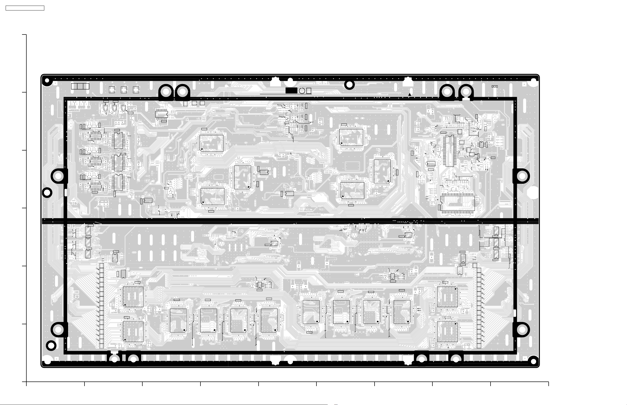
12.7. D-Board
6
5
4
3
2
D-BOARD (FOIL SIDE)
TZTNP010GYS
123
C003
C004
D002
LC023
R532
R538
LC026
R533
LC027
R695
R698
R701
R696
R697
R726
R732
R733
R728
R730
R822
R827
R828
R824
C002
D001
R062
Q010
R104
C024
R858
R054
Q002
R096
C029
R852
R043
R058
Q006
R100
C033
R518
R694
1
10
1
R723
10
R819
1
10
R826
LC028
R022
R021
C015
R048
R049
R047
Q011
Q009
C022
R103
IC006
16
C036
1
R859
R112
R039
Q001
C028
R110
Q005
C032
R520
R113
R040
R041
Q003
C023
R095
IC004
R094
16
1
R853
R109
R044
R045
Q007
R099
C021
16
1
8
IC005
R855
L002
IC560
C382
20
C512
C513
11
IC564
20
C397
C514
C515
11
IC510
20
C449
C510
C511
R862
11
R864
R652
R779
R686 R687
R683
R682
R679
R678
R850
R848 R654
R846
R844
R842
R840
R838
R836
R834
1
1
2
2
34
34
LC007
LC008
IC000
IC001
3
R027
4
R102
R101
C035
9
8
C049
R093
C027
9
8
C046
C182
R097
C031
9
R098
R857
C043
R861
R863
R020
R025
3
1
5
4
R019
R034
R038
C563
1
R860
C579
C184
10 11
C566
R206
1
C561
R854
C577
10
C570
1
C562
C578
C232
10
R856
C041
1
10
C426
C367
3
R018
R023
1
5
4
R017
C016
C014
L001
C042
C253
R433
IC021
R203
IC019
C564
C565
IC020
IC520
20
11
11
IC504
20
96
97
C376
C363
128
1
L554
96
97
C455
128
L504
C430
1
1
2
34
LC009
C040
C025
1
5
L003
IC002
R036
L019
R227
R226
C268
C573
R369
20
R290
R330
L018
C576
C261
C569
R194
R331
20
C571
R209
R329
C071
L017
C567
C574
11
R432
R118
20
R368
C255
C572
C265
R211
C277
R189
C575
11
R191
C568
R192
C287
20
D717
R293
IC047
1
R507
C522
C523
C524
10
1
C379
IC558
65
64
C371
IC512
C434
32
C457
65
64
32
C451
R366
R367
R186
8
9
R373
C222
R481
R495
C239
C243
R554
C279
R512
11
R438
R987
10
R506
R989
C377
R702
R703
C419
33
C368
C364
C420
C456
R830
R829
33
C435
C431
R309
1
16
IC202
C134
R372
C223
C224
C225
R479
R450
R497
R499
R484
R511
C249
R508
R500
Q021
C281
C280
R482
R494
R986
C533
R984
C534
R983
R982
C537
C536
R985
C535
L501
51
R761
R763
R765
R767
R769
80
81
R051
R310
R311
R375
R374
C275
R435
R417
C236
R405
R436
C246
R515
C166
C273
R526
R553
R528
C160
R400
C282
R398
R396
C531
C530
C532
R981
IC503
C418
3150
30
R798
1
100
R762
R764
R766
C414
R768
R053
R052
R502
C272
R337
IC209
80
81
R428
100
C172
1
R430
R431
R552
80
81
C153
100
1
R567
IC502
C410
50
51
C411
80
81
R793
R789
R785
R781
R032
TNPA1901
SEE REVERSE FOR ORDER NO.
C207
R468
R474
R540
R449
C197
C198
R444
C136
IC201
C289
R451
R404
R448
R317
C466
R427
51
50
C176
31
30
C170
C168
50
51
C135
51
50
80
81
C152
C144
C125
31
30
C130
R556
R569
R584
R562
R573
R583
C293
R571
C297
C311
R560
R559
R579
R580
C309
C303
C408
C498
C497
C427
100
50
31
30
51
R778
1
80
R794
R776
81
R790
R774
R786
R772
R770
R782
C423
C415
C416
31
30
IC200
1
100
C143
C124
R402
R403
C164
C165
C294
R561
C307
C312
C305
R734
R736
C398
R739
5
C403
8
IC516
C407
IC506
L036
C417
31
R799
51
30
C409
C412
1
80
100
R795
C413
R777
R791
R775
R787
R773
R783
R771
R460
R452
R458
C193
R461
R455
R459
C194
C465
C119
1
1011
IC707
C718
20
C323
C316
R613
R873
14
C463
IC404
1
C318
C317
R735
C401
C400
4
1
X500
IC507
50
C203
C212
R467
C204
C213
C211
R475
C206
R473
Q050
R463
R545
R469
C472
C476
R547
C479
C475
C238
L350
C230
C288
IC048
8
R874
R875
7
R876
R614
C404
C428
31
30
1
10081
C424
C471
C205
R542
C474
R541
R543
C226
R483
C233
R480
R498
R496
R501
R555
C283
R531
C284
11
20
R530
10
1
R504
R503
R993
R992
R991
C324
C315
C326
C325
C422
L502
C352
C421
51
R634
R636
R640
R644
R648
R796
R792
R788
R784
80
R031
R029
2
D
IC213
C215
IC214
C216
IC217
C227
R513
C254
C546
L026
50
IC061
R030
94V-0
D011
R119
C492
R955
R956
C601
C602
C600
C603
R890
R891
C173
C229
C228
C237
C248
C167
R517
C274
R527
R664
R617
R529
R509
C285
L551
C353
C161
R401
R399
C286
R397
C541
R568
C290
L450
C351
C343
31
50
51
30
R674
C344
1
80
R635
R639
10081
C347
81
R643
R647
R669
R665
R660
R656
C199
IC259
80
81
R429
100
1
80
81
C156
100
1
C304
R570
R574
R586
R582
C341
IC552
C360
100
51
50
C179
31
C171
30
C200
C138
IC251
R572
C306
R585
C120
R581
R563
C313
C310
C496
C495
R618
31
51
30
R651
1
80
R670
R649
R666
R645
R661
R641
R657
R637
C356
C348
C169
50
51
C137
51
50
80
81
C155
C127
C146
31
30
R565
R566
C298
R564
C314
C336
IC556
50
81
C349
31
30
IC250
1
100
C145
C126
C132
C319
R615
C308
C296
C295
R612
C340
C350
31
30
1
100
C345
R650
R646
R642
R638
R877
C327
14
C157
IC454
1
C329
C330
R607
C334
R608
R609
C331
5
8
IC057
L028
50
R675
51
C342
C346
80
81
R671
R667
R662
R658
C338
C333
4
C335
1
X004
IC557
C361
31
100
C357
L900
C076
R234
R228
C500
C501
C105
C923
C051
R137
C052
R271
R272
C103
R139
R881
Q013
C736
R306
C104
20
C102
R292
R307
IC703
C099
R286
R280
R158
R157
R145
C320
C328
8
R878
R879
R880
7
R616
C322
C321
C339
L550
L552
C354
C355
30
R672
R668
R663
R659
1
R150
C493
C904
C089
IC702
R231
C088
R239
R248
C927
R916
R255
C100
R882
C908
C096
11
10
1
IC704
R148
R332
R165
R149
R283
R205
R166
C097
R174
R172
R171
R177
R162
R333
C062
R176
R327
C063
C064
44
C065
R156
C058
C078
C081
IC705
1
L027
32
33
R700
R699
C372
64
65
C370
C369
C365
32
33
R832
R833
C453
64
65
C436
C432
R212
R214
C922
C920
R146
R179
R180
C921
C901
R202
R168
R167
R106
R282
R275
40
1
C101
D013
20
IC559
R962
R963
R287
C929
R365
R364
21
C086
R221
R233
R220
C079
R219
C080
C077
R238
R218
R334
D014
D015
R321
R315
R314
IC521
11
C527
C526
C525
20
IC555
11
20
C358
C378
1
128
97
96
C366
C458
IC513
1
128
97
96
C452
CR NO. 9
R322
R270
R250
Q903
R252
R213
R261
R303
R920
R262
R919
R921
R269
R264
R258
R263
R266
R267
R265
C924
R947
R289
1
R285
C932
C925
C098
4
R965
C930
R948
3
4
C933
R869
1
5
R870
R284
R281
C106
R362
R230
C084
R235
R254
R241
C373
C454
C433
IC909
R353
R288
R361
C116
R354
R355
R359
C117
R363
R356
R360
R243
C083
R256
C091
R300
C090
R259
R278
R257
23
C112
C113
22
R688
R690
R693
C517
R689
C516
R691
C383
R692
C519
R724
C518
R727
C396
R722
R725
R729
R731
R301
10
C520
R302
R304
R305
1
R653
10
1
C362
C429
R655
L553
L503
R831
C114
C115
R918
Q902
C926
R937
R954
C108
C109
R953
R945
8
R944
R950
R949
R946
IC907
R917
5
L005
R318
C910
R534
Q901
R320
R319
R441
R357
R358
C745
R141
R535
10
11
20
1
IC561
11
10
20
1
IC565
10
11
C521
C450
R780
R685
R684
R681
R680
R677
R676
R849
R847
R845
R843
R841
R839
R837
R835
1
20
R817
IC511
R820
R825
R818
R821
R823
1
ABCDEFGH I
52
Page 53
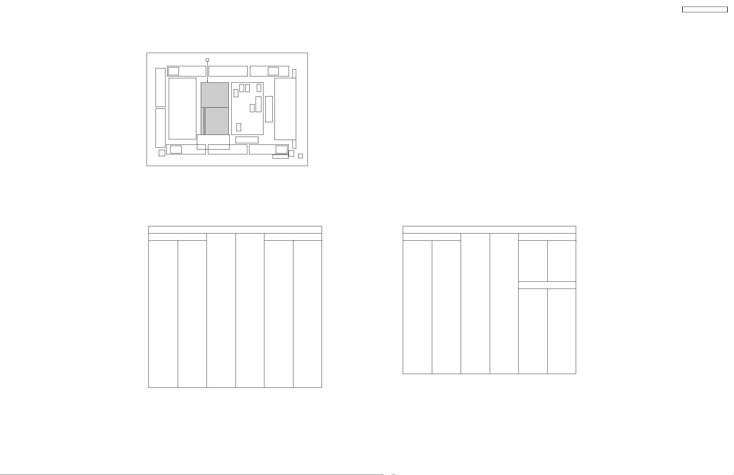
TH-50PHD3 / TH-50PHW3
D
PARTS LOCATION
D-BOARD (FOIL SIDE)
IC
IC000 B-5
IC001 B-5
IC002 B-5
IC005 B-4
IC019 B-4
IC020 B-4
IC021 B-5
IC047 B-4
IC048 E-4
IC061 E-1
IC067 G-2
IC200 D-4
IC201 D-3
IC202 C-5
IC209 D-5
IC213 E-5
IC214 E-5
IC217 E-5
IC251 F-4
IC259 F-5
IC260 G-4
IC404 E-3
IC454 G-3
IC502 D-2
IC503 C-2
ADDRESS INFORMATION
IC504 B-2
IC506 D-2
IC507 E-2
IC510 B-3
IC511 I-3
IC512 B-2
IC513 H-2
IC518 E-2
IC520 B-3
IC521 H-3
IC552 F-2
IC555 H-3
IC556 F-2
IC557 G-2
IC558 B-2
IC559 H-2
IC560 B-3
IC561 I-3
IC564 B-3
IC565 I-3
IC702 H-5
IC703 G-4
IC704 G-4
IC705 H-4
IC707 D-4
IC907 H-5
IC909 H-4
TRANSISTOR
Q001 B-4
Q002 A-4
Q003 B-4
Q005 A-4
Q006 B-4
Q007 B-4
Q009 B-5
Q010 A-5
Q011 B-5
Q013 G-4
Q021 C-4
Q050 E-5
Q901 I-4
Q902 H-5
Q903 H-5
PARTS LOCATION
D-BOARD (COMPONENT SIDE)
IC
IC003 H-3
IC007 H-4
IC008 H-4
IC009 H-5
IC010 H-3
IC012 H-4
IC014 F-3
IC015 G-5
IC016 G-5
IC017 G-5
IC018 H-3
IC023 H-3
IC024 E-5
IC036 F-5
IC068 C-2
IC093 G-5
IC204 F-5
IC206 F-5
IC207 E-5
IC210 F-5
IC211 E-5
IC212 E-5
IC215 E-5
IC223 F-5
IC225 G-4
IC226 E-3
IC254 D-4
ADDRESS INFORMATION
IC302 G-4
IC352 E-4
IC400 F-3
IC401 G-3
IC402 E-3
IC403 E-3
IC450 D-3
IC451 D-3
IC452 C-3
IC453 C-3
IC500 F-2
IC501 F-2
IC505 B-2
IC509 B-1
IC508 H-1
IC551 D-2
IC554 H-2
IC562 H-2
IC563 B-2
IC701 B-3
IC706 C-5
IC900 B-5
IC901 A-5
IC902 B-5
IC903 B-5
IC904 B-5
IC905 B-4
IC906 B-4
IC908 C-5
TRANSISTOR
Q014 B-4
Q015 F-5
Q016 C-4
Q017 G-5
Q018 G-5
Q019 E-5
Q020 E-5
Q022 C-4
TEST POINT
TPD1 F-2
TPD2 D-4
TPD3 G-4
TPD4 E-4
TPD5 F-3
TPD6 D-3
TPD7 D-3
TPD7 F-5
TPD8 F-3
TPD9 F-2
TPD10 D-3
TPD12 D-3
TPD20 H-5
TPD21 H-4
TPD22 H-4
53
Page 54
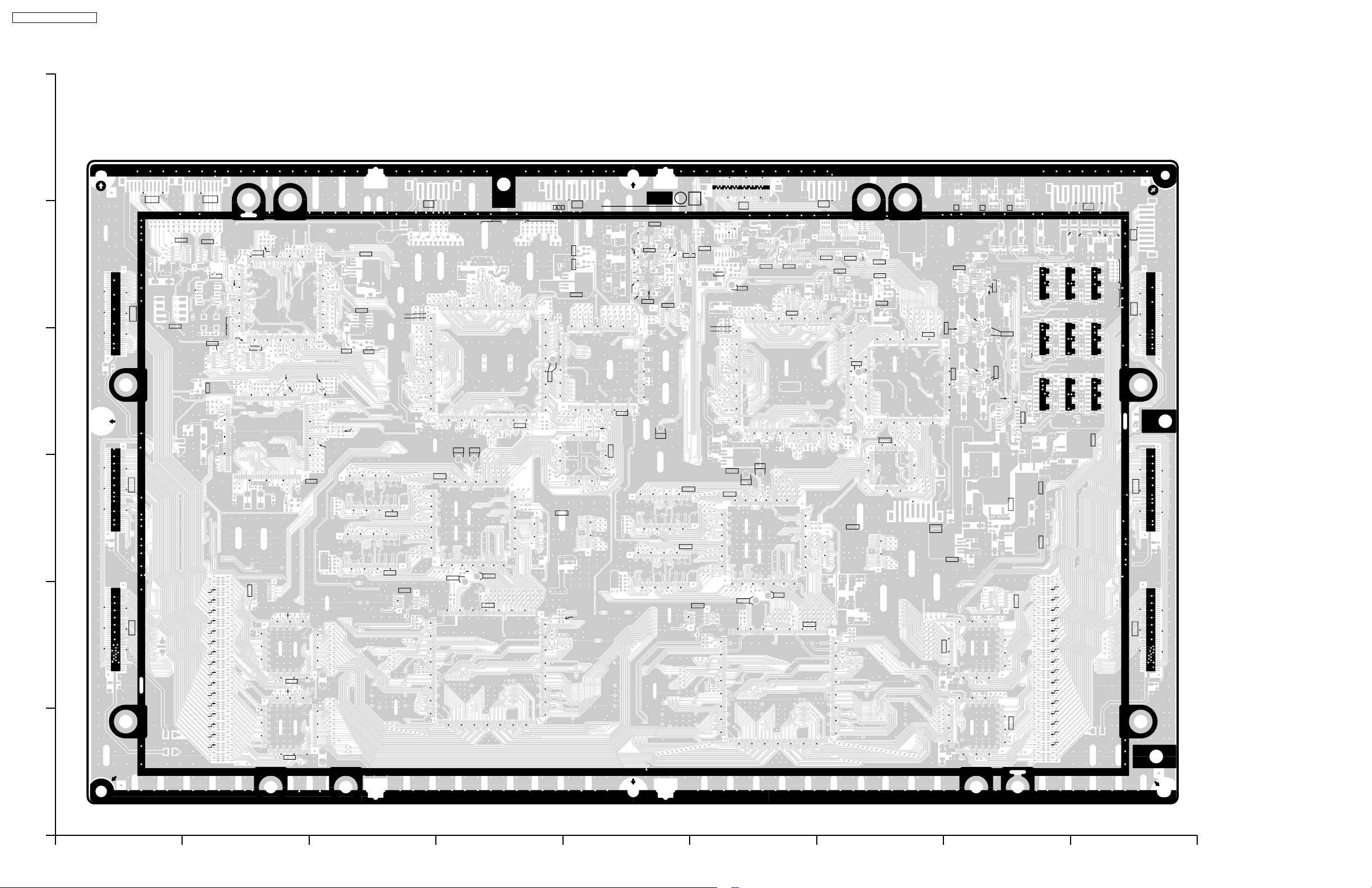
TH-50PHD3 / TH-50PHW3
6
D-BOARD (COMPONENT SIDE)
TZTNP010GYS
R002
R003
JK002
D21
R348
R345
R346
R347
R344
C122
5
L006
C121
D36
IC901
C375
C374
4
D35
3
C395
C394
D34
2
C444
C443
LC029
LC030
LC032
D20
R338
R339
R342
R343
R352
R340
R341
R349
R350
R351
IC903
IC904
C087
R215
R866
R867
R868
R865
R143
R142
R279
D012
LC025
C057
R966
IC902
R896
R964
X002
R967
R969
C110C111
R323
R308
IC905
R299
R335
R251
Q014
R260
C095
C094
R268
C056
C055
C092
R704
R706
R708
R710
R712
R714
R716
R718
R720
R797
R801
R802
R805
R806
R809
R812
R814
R816
R973
R974
R872
C934
C935
R204
IC900
IC906
R246
R232
R245
R236
R883
R253
X001
IC505
C425
C387
C440
R210
R185
C494
R164
R195
R276
R277
R229
C085
C082
R223
C093
D010
R140
C384
IC563
C390
C437
IC509
C447
R445
C075
R313
R193
R274
R273
R178
R182
R183
R184
R188
R197
R198
R196
R190
R151
R175
R161
R160
R173
R155
C060
IC701
R181
C053
R603
R601
R599
R604
R602
R600
C386
L556
C439
IC908
R550
R224
R551
R225
L903
R237
C107
Q016
C068
C066
C073
C070
R536
R163
R159
R153
R605
R593
R606
R594
L506
C502
C503
IC706
R312
Q022
R154
IC452
IC453
C337
D4
R135
R134
R132
R133
LC024
R138
C050
D007
R407
R411
R423
R413
R421
R416
R384
C141
C131
IC058
R624
C332
R625
R629
R632
R136
D006
D005
D008
R426
R419
R380
C159
IC450
TPD12
R611
R628
R633
R114
R116
D009
C150
C148
L252
L254
R476
C214
C178
C154
R381
R385
TPD6TPD7
R558
C559
R887
R888
TPD10
R620
R621
R619
IC551
CR NO. 9
R124
R115
R117
R122
R123
D004
C190
C191
R472
C180
IC254
C142
R125
C054
D003
C133
R424
R409
R437
TPD2
R393
R392
R387
R990
C540
R576
R578
IC451
C292
L451
R623
R626
R630
R627
R631
D2
R377
Q019
Q020
IC024
C547
C542
C300
C302
R622
TNPA1901
C217 C218
C208
C201
R466
C210
R376
R478
C543
R462
C202
C473
C470
R544
C477
IC352
R516
R514
C544
IC226
C545
R597
R595
R591
R589
R587
R598
R596
R592
R590
R588
R465
IC212
IC215
R447
2
D
IC211
C195
C196
C478
IC207
R446
R485
C240
C244
C256
C266
C278
TPD4
R013
C460
R012
C010
R454
R453
C461
IC223
R457
IC210
R456
C481
C059
R549
R548
C192
R422
R420
IC402
IC403
IC500
C402
R751
C399
R752
R756
R759
D1
R014
R144
R170
C069
R406
R410
R412
R414
C162
R738
R755
R760
LC033
R015
R121
C490
C491
R120
L010
C242
C174
C462
R443
C061
R147
R152
Q015
C067
R169
TPD1
C147
C149
R425
R418
R382
R378
C139
C158
C129
L205
C163
IC014
TPD8
IC400
R886
TPD11
R747
R748
C188
IC036
IC206
R470
C209
C175
R379
C151
R383
TPD5
C558
C123
R557
R885
TPD9
R746
D3
R079
R080
R108
R105
R336
IC015
R298
R440
C189
C187
R464
C177
IC204
C140
R575
R577
R745
IC501
R078
C276
IC016
R294
R442
IC093
C480
C291
L400
R757
IC017
Q017
R439
X003
C185
R434
R296
Q018
R408
R415
L300
TPD3
R388
R389
R386
IC401
L401
C299
C301
L500
C406
C405
R750
R753
R749
R754
R758
L009
R371
C128
R370
C219
C220
C221
R477
IC225
DMM3
JK001
R006
R016
R
GB
R009
R011
C013
C269
C039
R249
R316
IC009
C270
C264
C267
C262
R247
IC008
C263
IC302
C257
IC007
C258
R510
C506
LC022
C505
C485
C484
D6
IC018
IC562
L555
C389
L505
C446
R244
C259
R242
R240
C251
C252
C074
C072
C018
C489
R297
R295
C483
C464
C482
C359
C385
C393
C438
C448
1
R001
JK003
R004
R005
R008
R007
R010
C011
C012
R024
C038
R037
R028
C037
R222
TPD20
C504
TPD21
R217
C260
TPD22
R324
R216
C560
R208
R326
IC010
C009
L044
C388
IC508
C445
R035
R033
R076
R091
LC020
C034
R068
R291
C026
R083
LC016
R325
C030
R072
R207
R087
IC012
R111
C047
R328
C005
C459
L008
IC554
C118
C001
IC023
C019
C017
IC003
R705
R815
D5
LC001
LC002
C006
R026
R064
R075
R090
R056
R067
R082
R060
R071
R086
R707
R709
R711
R713
R715
R717
R719
R721
R800
R803
R804
R807
R808
R810
R811
R813
LC004
LC005
LC003
C007
R063
R074
R089
LC018LC019
LC010LC011LC012
R055
R066
R081
LC014
LC015
R059
R070
R085
R107
IC022
C020
LC031
D7
LC006
C008
R126
R127
R128
R129
R130
D31
R131
DMM1
C381
C380
D32
C391
C392
R537
D33
C441
C442
DMM2
ABCDEFGH I
54
Page 55
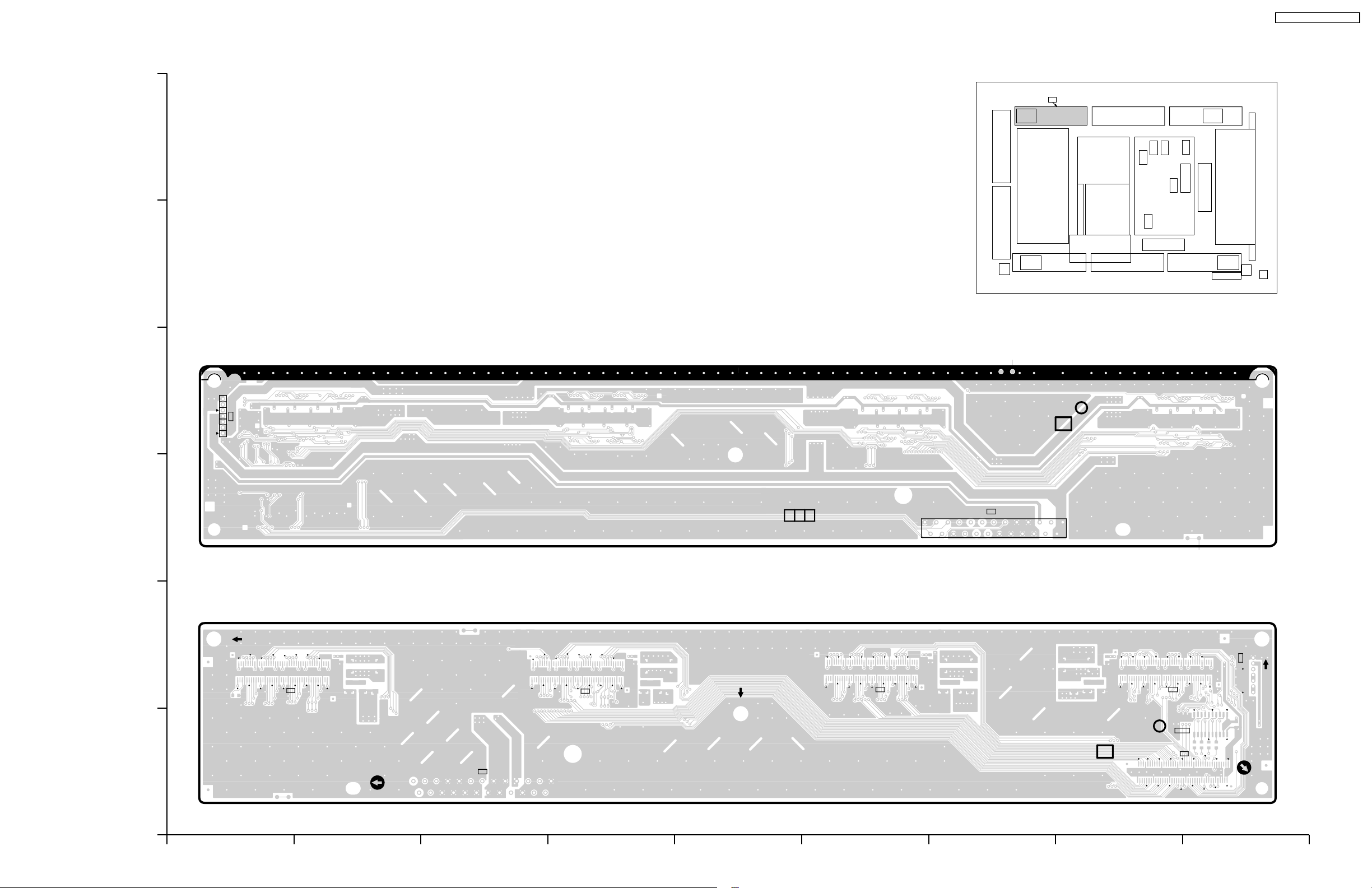
12.8. C1-Board
6
5
C1-BOARD (FOIL SIDE)
TNPA1914
TH-50PHD3 / TH-50PHW3
C1
4
3
7
5
C13
1
5
123
1
2
TNPA1914 2
SEE REVERSE FOR ORDER NO.
C12
15
10
20
C1
25
24
C1-BOARD (COMPONENT SIDE)
TNPA1914
2
L7108
L7105
C7105
R7105
CA1
L7101
D7101
C7110
C7111
CA2
L7102
C7104
C7113
L7106
D7102
C7112
CA3
C7108
L7107
C7115
L7103
D7103
C7114
L7104
C7109
C7117
C7116
D7104
CA4
C13
5
TNPA1914 2
C1
1
20
C12
15
5
10
IC7101
R7103
R7102
R7104
C11
C7103
R7101
ABCDEFGH I
55
Page 56
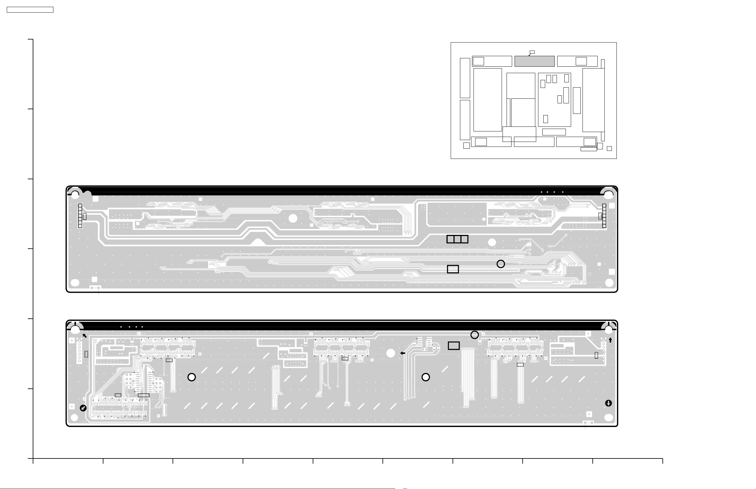
TH-50PHD3 / TH-50PHW3
12.9. C2-Board
6
5
C2
C2-BOARD (FOIL SIDE)
TNPA1915
1
4
C23
5
7
7
5
C22
1
123
TNPA1915
1
C2
SEE REVERSE FOR ORDER NO.
3
C2-BOARD (COMPONENT SIDE)
TNPA1915
IC7132
C7137
5
2
C22
D7131
C7141
C7140
L7131
L7134
R7131
R7132
R7133
R7134
C21
C7134
IC7131
R7141
R7142
R7143
R7144
CA5
D7132
L7132
C7142
C7143
C7136
L7135
CA6
C7146
R7150
TNPA1915
C2
R7148
R7149
1
C7144
C7145
C7139
L7136
CA7
D7133
5
L7133
C23
1
ABCDEFGH I
56
Page 57
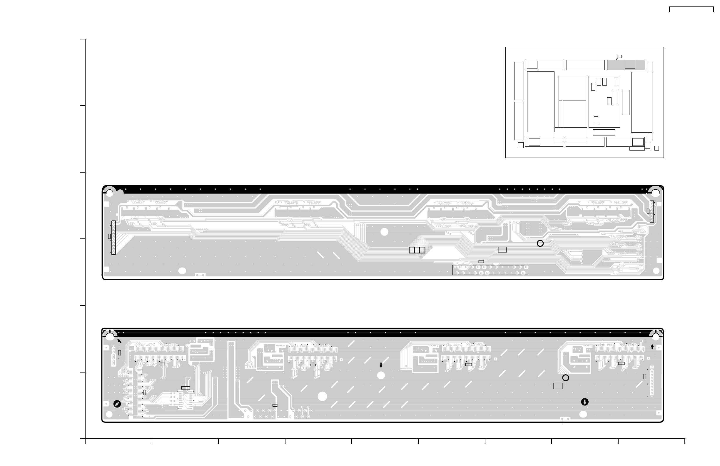
12.10. C3-Board
6
5
C3-BOARD (FOIL SIDE)
TNPA1916
TH-50PHD3 / TH-50PHW3
C3
4
11
C34
5
1
3
123
C35
5
1
2
TNPA1916 2
C3
SEE REVERSE FOR ORDER NO.
15
25
24
2010
17
C33
5
C3-BOARD (COMPONENT SIDE)
TNPA1916
2
D7161
C7166
C7167
C7163
C33
5
CA8
L7161
L7165
C7162
C7168
C7169
D7162
L7162
L7166
CA9
C7164
D7163
C7170
C7171
L7163
L7167
CA10
D7164
L7164
C7165
C7172
C7173
L7168
CA11
R7165
C7161
C31
1
R7161
R7162
R7163
R7164
IC7161
20
C35
15 5
10
TNPA1916 2
C3
C34
5
ABCDEFGH I
57
Page 58
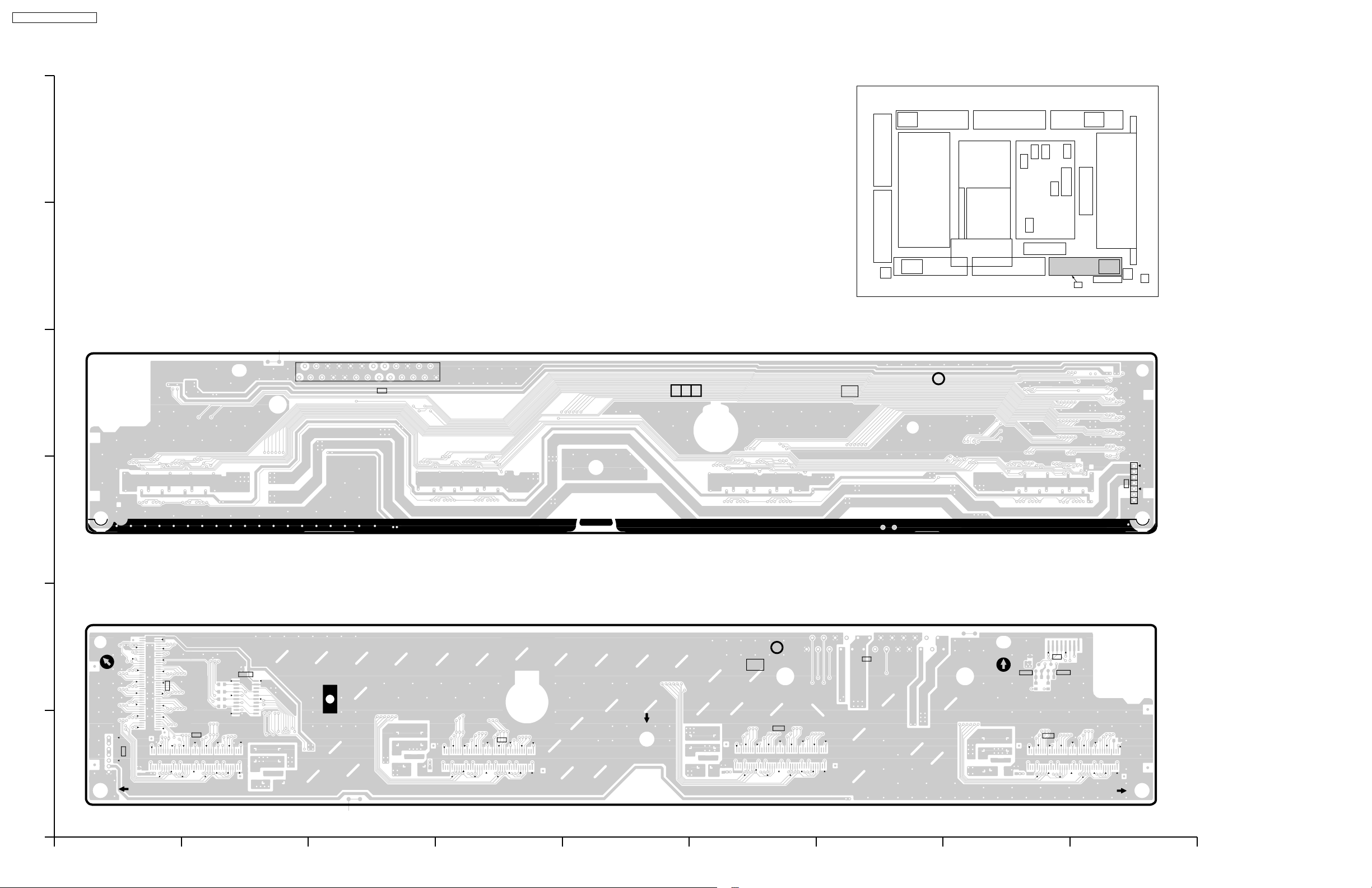
TH-50PHD3 / TH-50PHW3
12.11. C4-Board
6
5
C4-BOARD (FOIL SIDE)
TNPA1917
C4
20
24
10
2
25
4
15
C42
1
5
123
TNPA1917 2
C4
SEE REVERSE FOR ORDER NO.
1
C43
5
7
3
C4-BOARD (COMPONENT SIDE)
TNPA1917
10 20
2
C7263
C41
R7265
R7266
R7267
R7268
IC7261
C4MM1
TNPA1917 2
C4
5
15
C42
C44
C7266
Q7261
R7276
Q7262
R7278
R7275
R7277
CB8
L7261
C43
5
1
C7262
L7265
D7261
C7267
C7268
L7262
D7262
L7266
C7269
C7270
C7261
CB9
L7263
D7263
L7267
C7271
C7272
C7265
CB10
L7264
D7264
C7273
C7274
CB11
L7268
C7264
R7273
ABCDEFGH I
58
Page 59
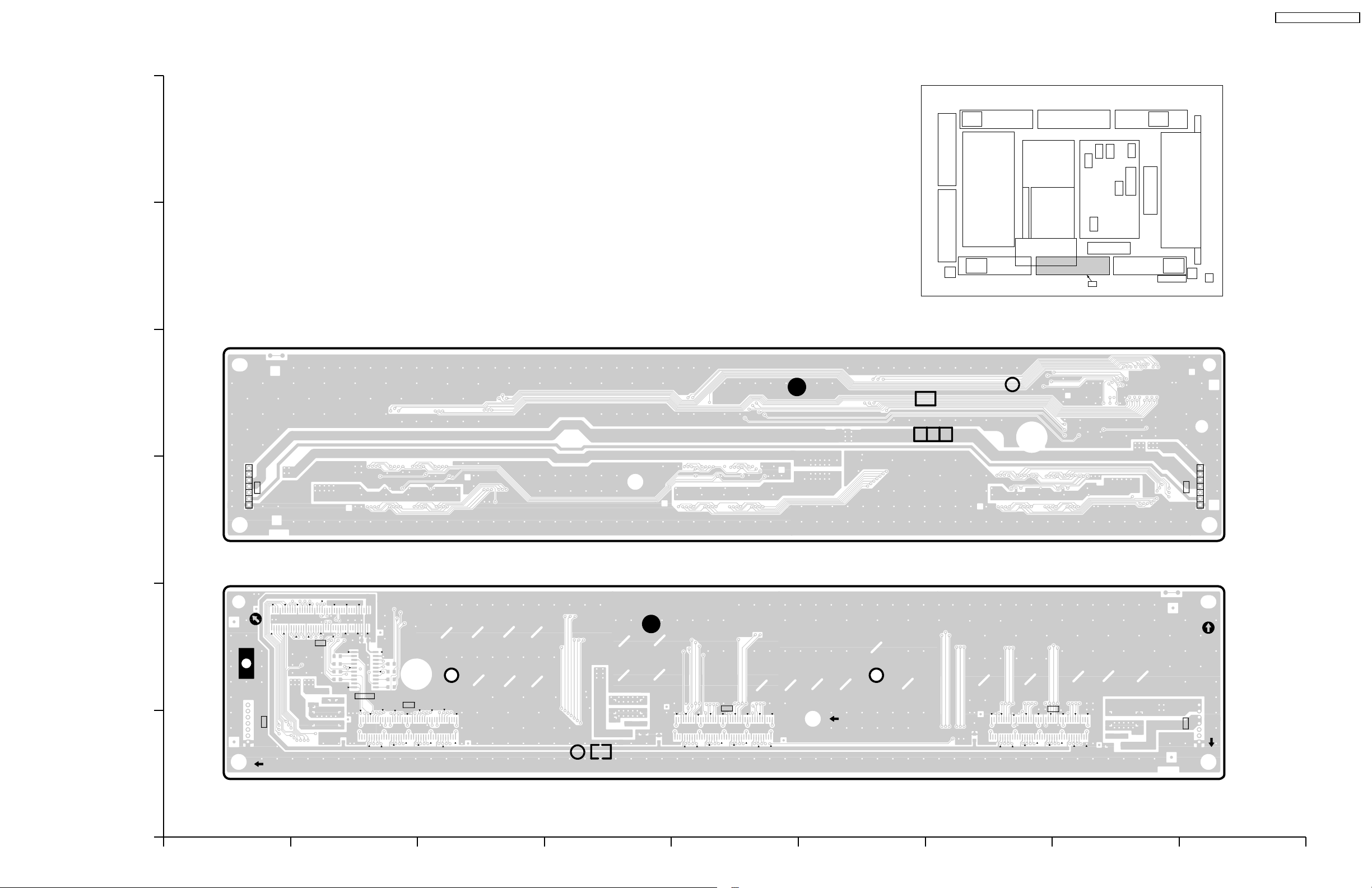
12.12. C5-Board
6
5
C5-BOARD (FOIL SIDE)
TNPA1918
TH-50PHD3 / TH-50PHW3
C5
4
C53
5
7
C5
SEE REVERSE FOR ORDER NO.
2
1
3
TNPA1918
1
71
5
C52
1
3
C5-BOARD (COMPONENT SIDE)
TNPA1918
D7231
C51
R7237
R7238
R7239
C7235
L7231
2
C5MM1
5
C52
R7236
C7236
C7233
R7251
R7252
R7253
R7254
IC7231
L7234
C7232
CB5
TNPA1918
L7232
D7232
C5
1
C7237
L7235
C7238
C7231
CB6
C7234
CB7
L7236
C7240
C7239
L7233
D7233
C53
5
1
ABCDEFGH I
59
Page 60
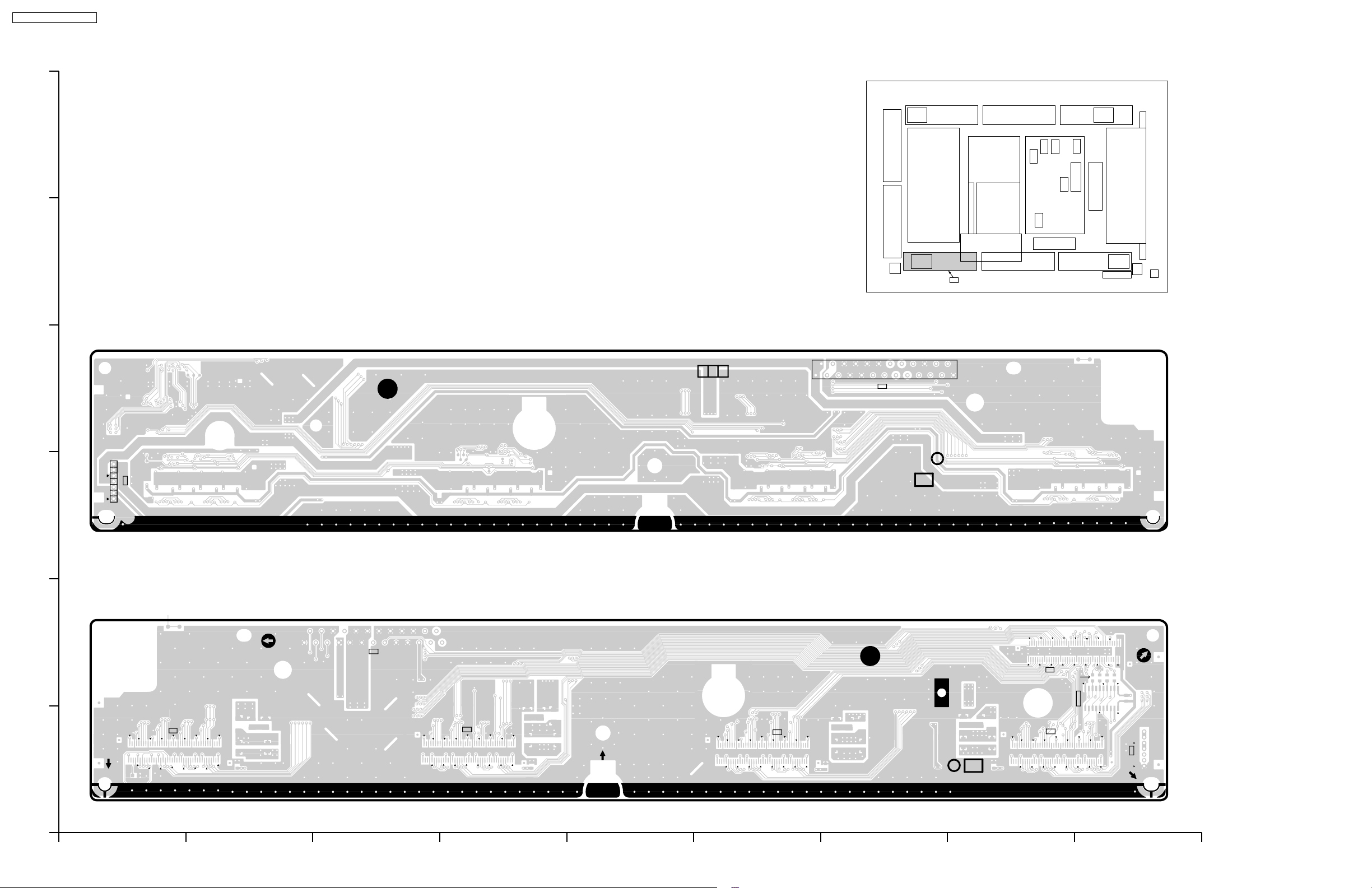
TH-50PHD3 / TH-50PHW3
12.13. C6-Board
6
5
C6-BOARD (FOIL SIDE)
TNPA1919
4
123
C6
20
24
25
10
15
C62
2
1
5
7
5
C63
1
TNPA1919
SEE REVERSE FOR ORDER NO.
2
C6
3
C6-BOARD (COMPONENT SIDE)
TNPA1919
10
2
C7207
D7201
CB1
1
R7205
C7206
L7205
L7201
C7202
5
C62
20
15
C61
R7207
R7206
R7208
R7209
D7202
C7208
C7209
CB2
L7206
L7202
C7201
CB3
C7210
C7211
D7203
L7207
C7205
L7203
C6MM1
TNPA1919
C7213
C7212
D7204
L7204
L7208
2
C6
C7204
IC7201
CB4
C7203
5
C63
ABCDEFGH I
60
Page 61
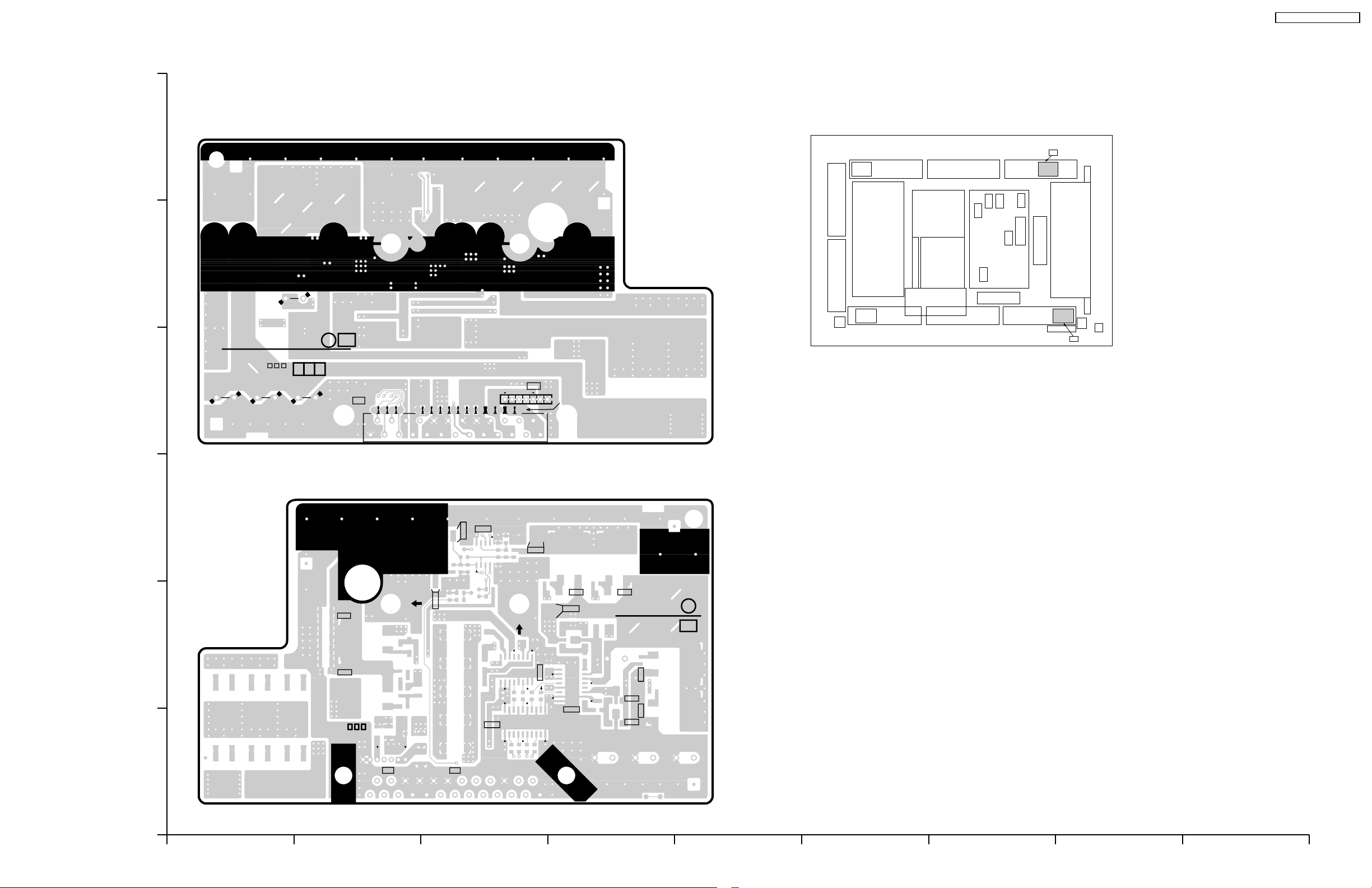
12.14. C7-Board
C7-BOARD (FOIL SIDE)
TNPA1993
6
5
TH-50PHD3 / TH-50PHW3
C7
C332
TNPA199 2
C7
C7
SEE REVERSE FOR ORDER NO.
CR No.7
4
C333
C301
123
C303
C7MM1
C71
TP319
TP321
TP320
TP318
TP317
TP316
TP315
TP314
TP313
TP312
TP311
TP310
TP308
2
1
TP309
C72
TP305
1
TP304
7
24
25
C7-BOARD (COMPONENT SIDE)
TNPA1993
3
C319
C318
2
L320
D320
L313
L316
L321
D316
L318
L312
C317
C316
C315
L315
L317
L319
L322
1
D314
D317
D321
L314
R317
D315
CRNo.7
L323
C7MM2
Q311
R314
Q312
D319
D318
R313
R315
R316
R305
C302
L301
C72
TP322
L325
D324
L326
L327
C314
L303
C308
IC304
R329
TP303
D323
R335
R336
R331
C331
R330
C71
C329
TP301
R327
R328
C328
R332
C330
R333
D322
C312
D311
C311
D312 D313
L328
C327
IC301
L329
R322
D326
C313
IC302
R321
R311
R320
R312
R304
R301
R302
R303
R323
Q313
TP302
R338
Q317Q318
C320
IC303
D327
D302
R337
C321
C322
R339
C303
Q314
TNPA1993
C332
R324
R340
Q315
R325
Q319
Q316
Q320
C301
2
C7
C333
C7MM1
ABCDEFGH I
61
Page 62
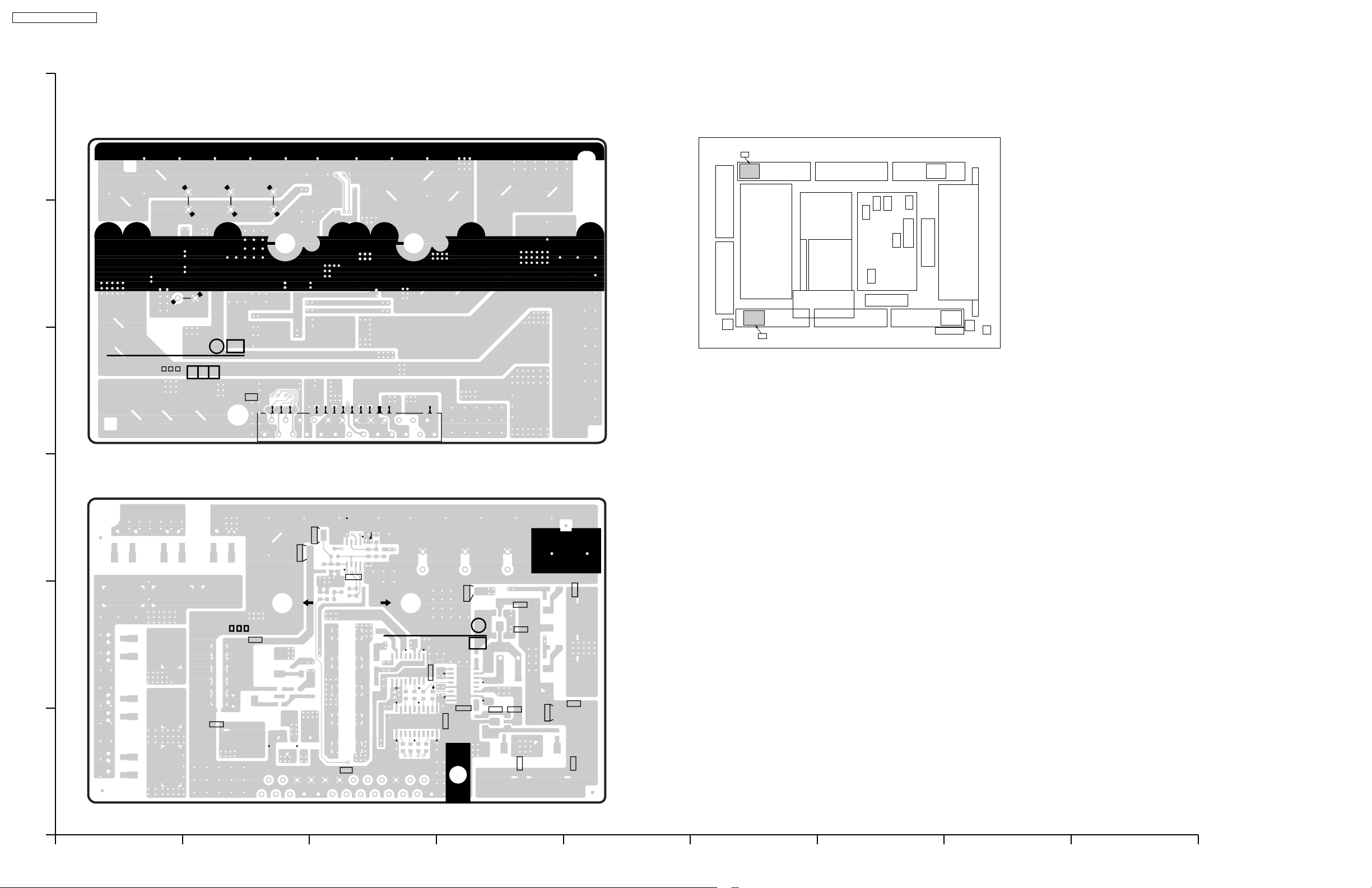
TH-50PHD3 / TH-50PHW3
12.15. C8-Board
C8-BOARD (FOIL SIDE)
TNPA2277
6
C8
C401
C403
C433
5
C432
C8
2
TNPA2277
SEE REVERSE FOR ORDER NO.
CR No.7
1
4
C8
2
3
TP417
TP418
TP419
TP420
TP421
C81
2
C8MM1
1
TP416
TP415
TP414
TP413
TP412
TP411
TP410
TP408
TP409
TP405
TP404
24
25
C8-BOARD (COMPONENT SIDE)
TNPA2277
3
TP403
L417
L416
D416
L412
2
1
L413
L419
L418
L423
L422
L420
D420
D414
D417
L421
CRNo.7
C419
C418
C417
C416
C415
R417
D421
L415
L414
D415
Q411
D419
R416
D418
R415
Q412
R405
C408
L403
D423
TP422
R435
R436
C430
R431
C431
R430
D424
R414
C414
R413
C402
L401
C429
R429
R427
R428
C428
IC404
R432
R433
D422
L425
C81
L426
D413
L427
D412
L428
L429
D411
TNPA2277
C411
C427
C403
C412
C413
IC402
R421
R420
R411
R412
R401
R402
R403
R404
C401
TP401
C8
C420
IC403
IC401
R440
C8MM1
C433
D426
R422
Q418
2
R437
Q420
R439
R438
Q417
C432
D427
C421
D402
C422
Q419
R425
Q416
Q413
R423
Q414
TP402
R424
Q415
ABCDEFGH I
62
Page 63
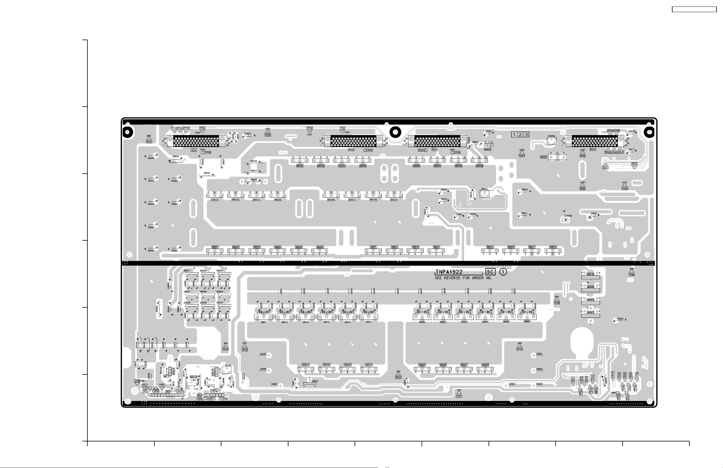
12.16. SC-Board
6
SC-BOARD (FOIL SIDE)
TNPA1922
5
TH-50PHD3 / TH-50PHW3
4
3
2
1
ABCDEFGH I
63
Page 64
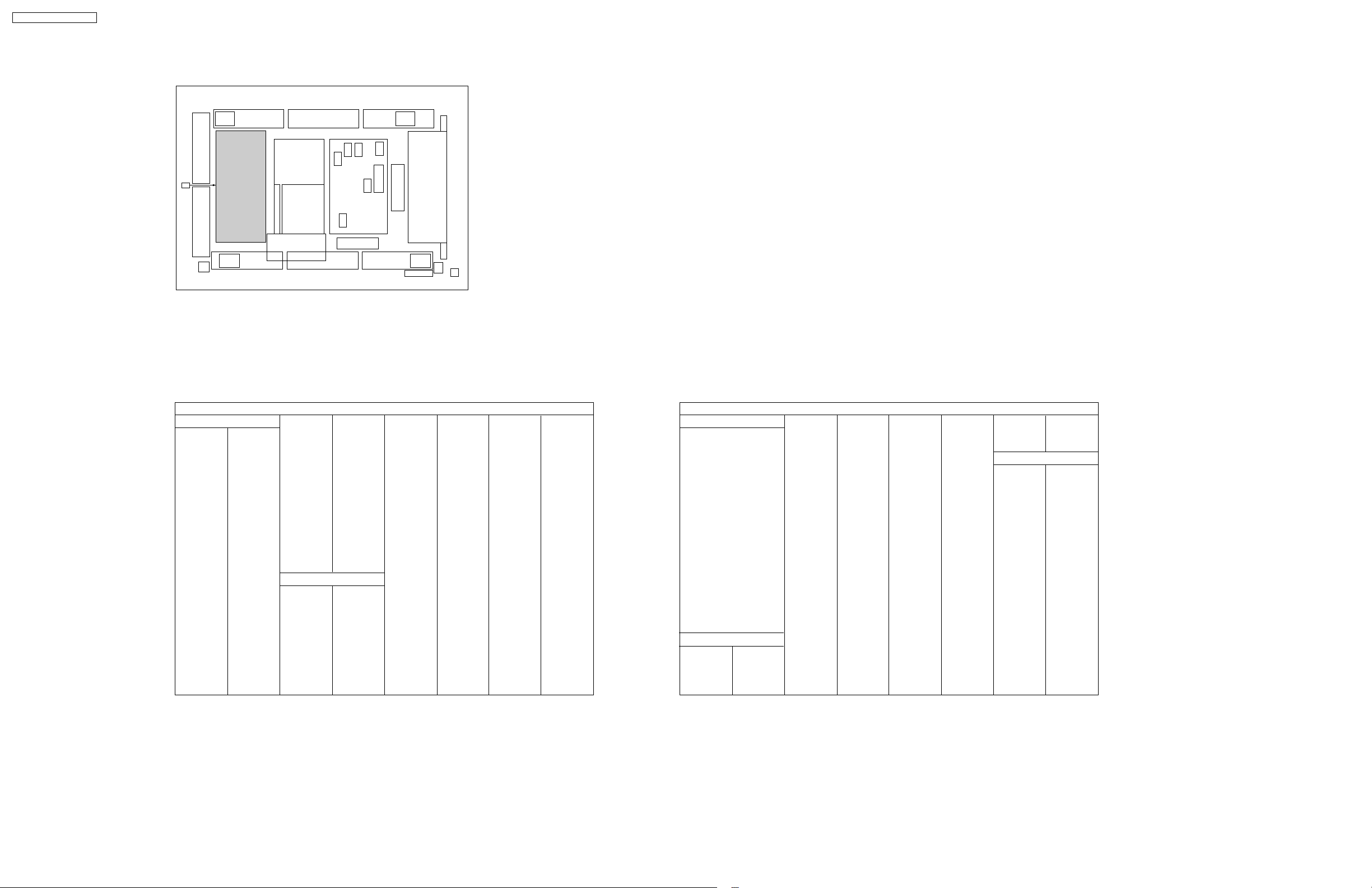
TH-50PHD3 / TH-50PHW3
SC
PARTS LOCATION
SC-BOARD (FOIL SIDE)
TRANSISTOR
Q6510 F-5
Q6522 B-4
Q6523 C-4
Q6524 C-4
Q6525 C-4
Q6526 D-4
Q6527 D-4
Q6528 E-4
Q6529 E-4
Q6531 G-5
Q6532 D-5
Q6533 D-5
Q6534 D-5
Q6535 E-5
Q6536 E-5
Q6537 F-5
Q6538 F-5
Q6539 F-5
Q6601 B-3
Q6602 C-3
Q6603 C-3
Q6604 C-3
Q6605 D-3
Q6606 D-3
Q6607 H-2
Q6608 H-3
Q6609 H-3
Q6610 H-3
Q6611 E-3
Q6612 E-3
ADDRESS INFORMATION
Q6613 E-3
Q6614 F-3
Q6615 F-3
Q6615 G-3
Q6616 G-3
Q6617 G-3
Q6618 G-3
Q6621 D-2
Q6622 D-2
Q6623 D-2
Q6624 E-2
Q6625 F-2
Q6626 F-2
Q6627 F-2
Q6628 F-2
Q6648 B-1
Q6649 B-2
Q6650 B-2
TEST POINT
TP1 A-1
TP2 A-1
TP3 B-1
TP4 B-1
TP5 B-1
TP6 B-1
TP7 B-1
TP8 B-1
TP9 B-1
TP10 H-1
TP11 H-1
TP12 H-1
TP13 H-1
TP14 H-1
TP15 H-1
TP16 H-1
TP17 H-1
TP18 I-1
TP19 I-1
TP20 I-1
TP21 I-1
TP22 H-1
TP23 I-1
TP24 I-1
TP25 I-1
TP26 H-5
TP27 G-5
TP28 F-5
TP29 I-4
TP30 H-4
TP31 D-5
TP32 D-5
TP33 C-5
TP34 B-5
TP35 B-5
TP36 I-3
TP37 F-1
TP38 A-1
TP39 G-3
TP40 G-2
TP41 E-1
TP42 H-1
TP43 C-2
TP44 C-2
TP45 A-5
TP47 F-5
TP48 B-5
TP49 I-5
TP50 B-5
TP51 H-5
TP52 B-5
TP53 H-5
TP54 H-5
TP55 H-5
TP56 H-5
TP57 H-5
PARTS LOCATION
SC-BOARD (COMPONENT SIDE)
IC
IC6500 A-5
IC6501 A-5
IC6502 B-4
IC6503 A-4
IC6504 B-4
IC6505 A-5
IC6506 B-5
IC6507 D-4
IC6509 B-4
IC6510 D-5
IC6511 F-5
IC6512 A-4
IC6521 D-4
IC6531 C-5
IC6541 B-4
IC6601 F-3
IC6602 E-1
IC6603 D-1
IC6604 C-3
IC6605 B-2
IC6606 A-2
IC6607 B-2
IC6608 G-2
TRANSISTOR
Q6511 G-5
Q6512 G-5
Q6513 E-4
Q6514 F-4
Q6515 C-5
ADDRESS INFORMATION
Q6516 E-5
Q6517 B-4
Q6518 D-5
Q6519 D-5
Q6521 C-4
Q6522 G-4
Q6523 G-4
Q6524 G-4
Q6525 G-4
Q6526 F-4
Q6527 E-4
Q6528 A-3
Q6528 E-4
Q6529 E-4
Q6531 B-5
Q6532 F-5
Q6533 F-5
Q6534 F-5
Q6535 E-5
Q6536 D-5
Q6537 D-5
Q6538 D-5
Q6539 D-5
Q6541 C-4
Q6542 B-4
Q6543 B-4
Q6545 A-4
Q6546 A-4
Q6601 G-3
Q6602 G-3
Q6603 G-3
Q6604 G-3
Q6605 F-3
Q6606 F-3
Q6607 B-2
Q6608 B-3
Q6609 B-3
Q6610 B-3
Q6611 E-3
Q6612 E-3
Q6613 D-3
Q6614 D-3
Q6615 C-3
Q6616 C-3
Q6617 C-3
Q6618 B-3
Q6621 F-2
Q6622 F-2
Q6624 E-2
Q6625 D-2
Q6626 D-2
Q6627 D-2
Q6628 C-2
Q6631 G-3
Q6632 G-3
Q6633 F-3
Q6634 F-3
Q6635 E-3
Q6636 E-3
Q6641 F-1
Q6642 F-1
Q6643 D-1
Q6644 E-1
Q6645 B-3
Q6646 B-3
Q6648 H-1
Q6649 H-2
Q6650 H-1
TEST POINT
TP15V H-1
TPSC1 G-5
TPSC2 F-1
TPVAD H-1
TPVbk H-1
TPVscn H-5
TPVset H-2
64
Page 65
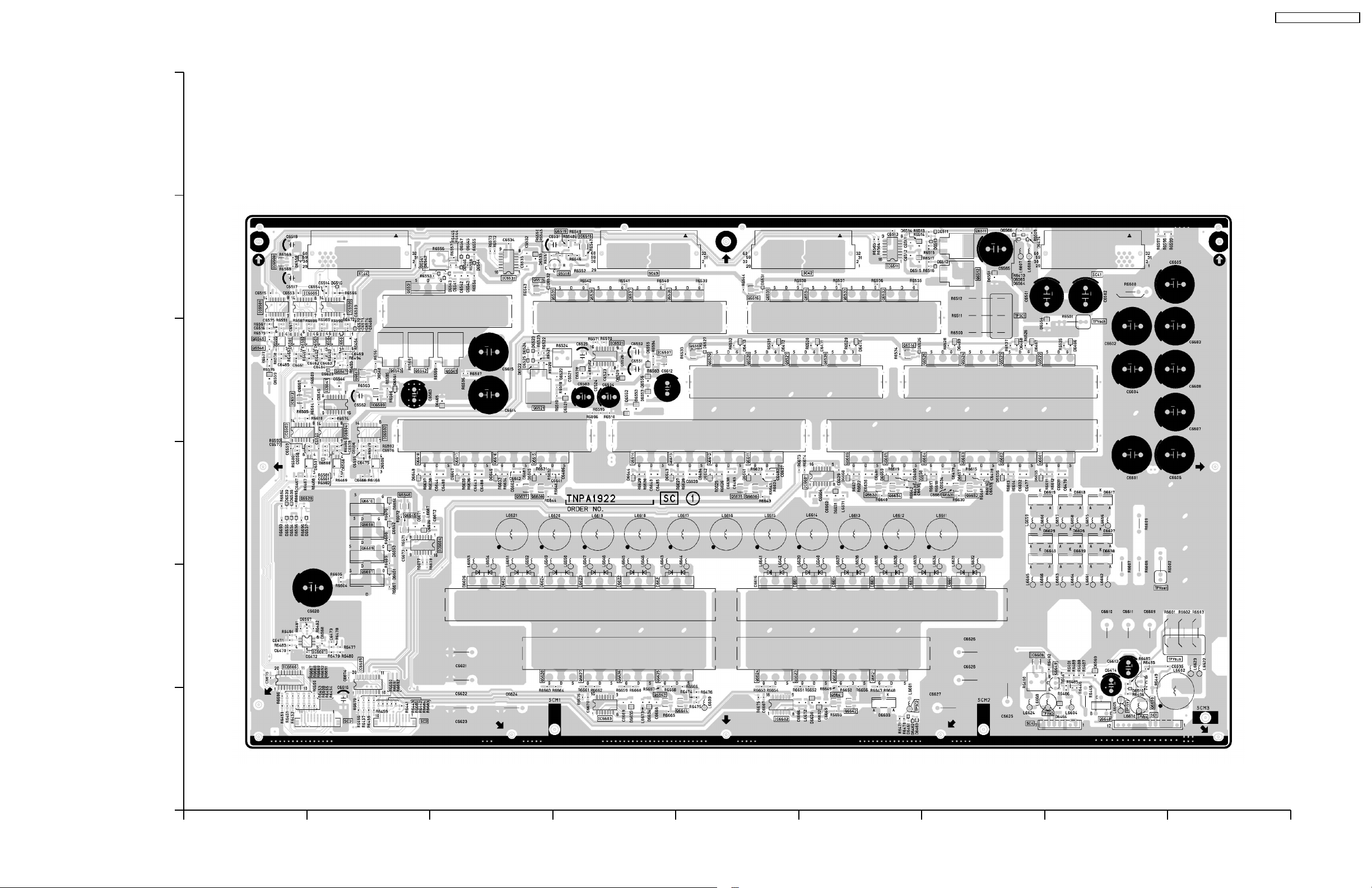
TH-50PHD3 / TH-50PHW3
6
SC-BOARD (COMPONENT SIDE)
TNPA1922
5
4
3
2
1
ABCDEFGH I
65
Page 66
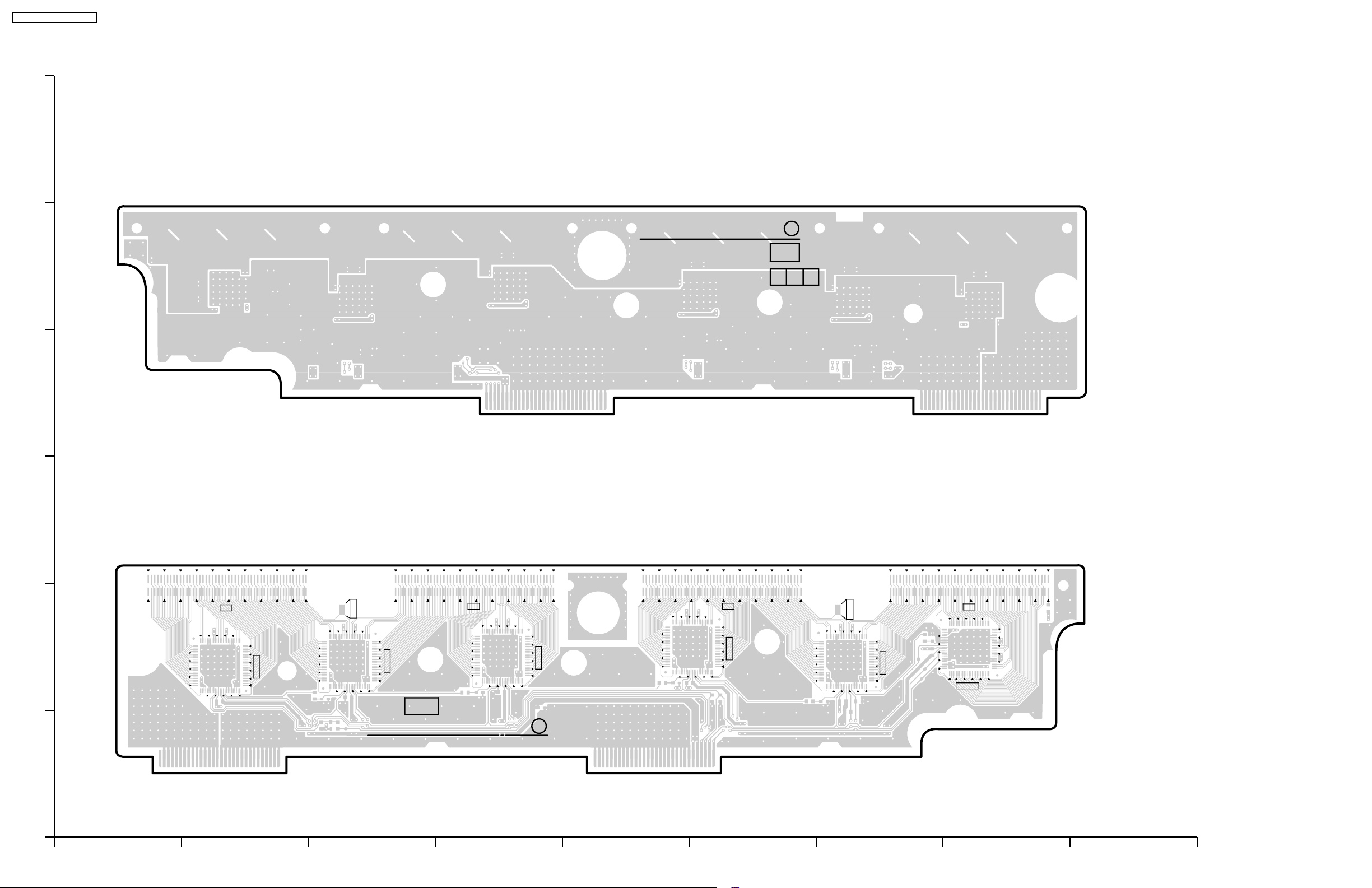
TH-50PHD3 / TH-50PHW3
12.17. SD-Board
6
SD-BOARD (FOIL SIDE)
TNPA1921
TNPA1921
SEE REVERSE FOR ORDER NO.
1
SD
5
4
3
SD-BOARD (COMPONENT SIDE)
21
3
TNPA1921
SD1
TPSD1
SD2
2
C6422
IC6411
R6422
D6413
C6421
D6412
C6423
R6421
TP5
TNPA1921
IC6412
SD
R6423
D6414
C6424
D6411
1
IC6413
R6424
D6415
C6425
C6429
SD3
IC6414
C6428
R6425
D6416
C6426
TPSD2
R6428
R6427
IC6415
SD4
D6417
R6426
C6427
TP7
TP6
TP8
IC6416
R6437
1
ABCDEFGH I
66
Page 67
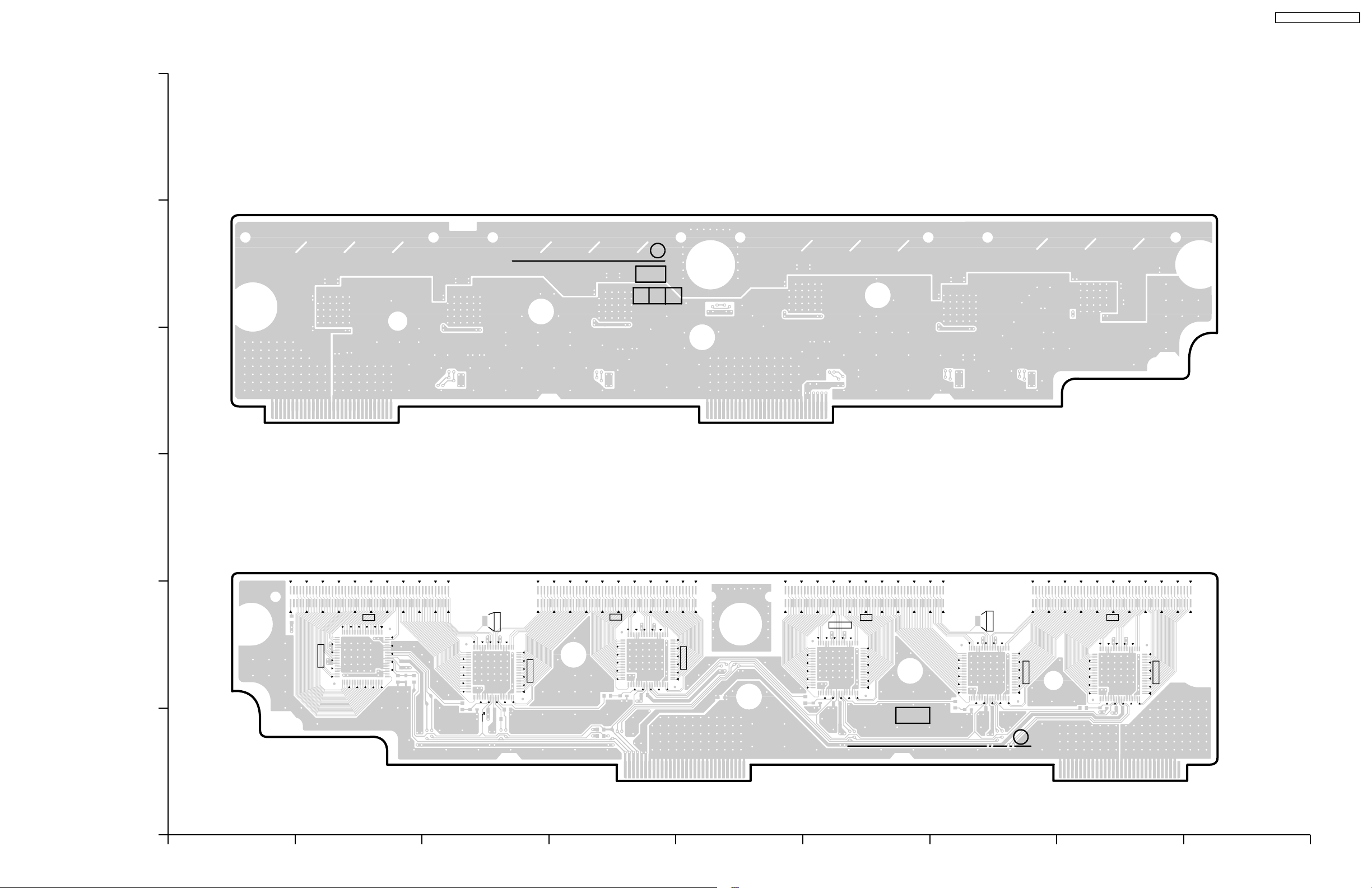
12.18. SU-Board
6
SU-BOARD (FOIL SIDE)
TNPA1920
TH-50PHD3 / TH-50PHW3
TNPA1920
5
SEE REVERSE FOR ORDER NO.
1
SU
321
4
3
SU-BOARD (COMPONENT SIDE)
TNPA1920
SU2
SU3 SU4
IC6404
TPSU2
R6410
SU1
TPSU1
2
C6411
C6401
D6402
R6401
TP4
TP1
TP2
R6402
D6403
C6402
R6408
R6407
IC6402
C6412
C6413
R6403
D6404
C6403
TP3
IC6403
D6401
R6404
D6405
C6404
SU
TNPA1920
D6406
R6405
C6406
IC6405
R6406
D6407
C6407
IC6406
1
IC6401
1
ABCDEFGH I
67
Page 68
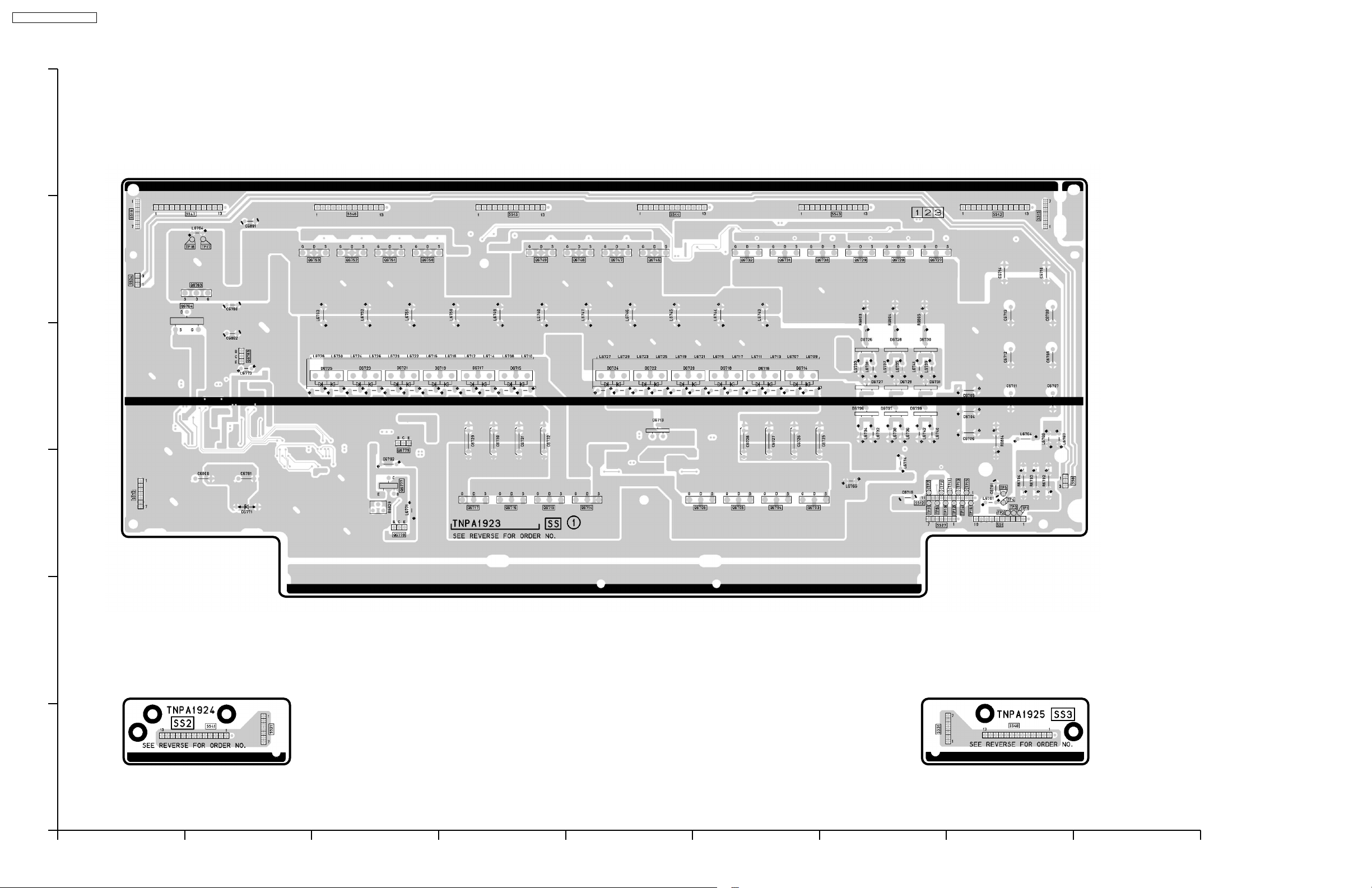
TH-50PHD3 / TH-50PHW3
12.19. SS, SS2 and SS3-Board
6
SS-BOARD (FOIL SIDE)
TNPA1923
5
4
3
2
SS2-BOARD (FOIL SIDE)
TNPA1924
SS3-BOARD (FOIL SIDE)
TNPA1925
1
ABCDEFGH I
68
Page 69
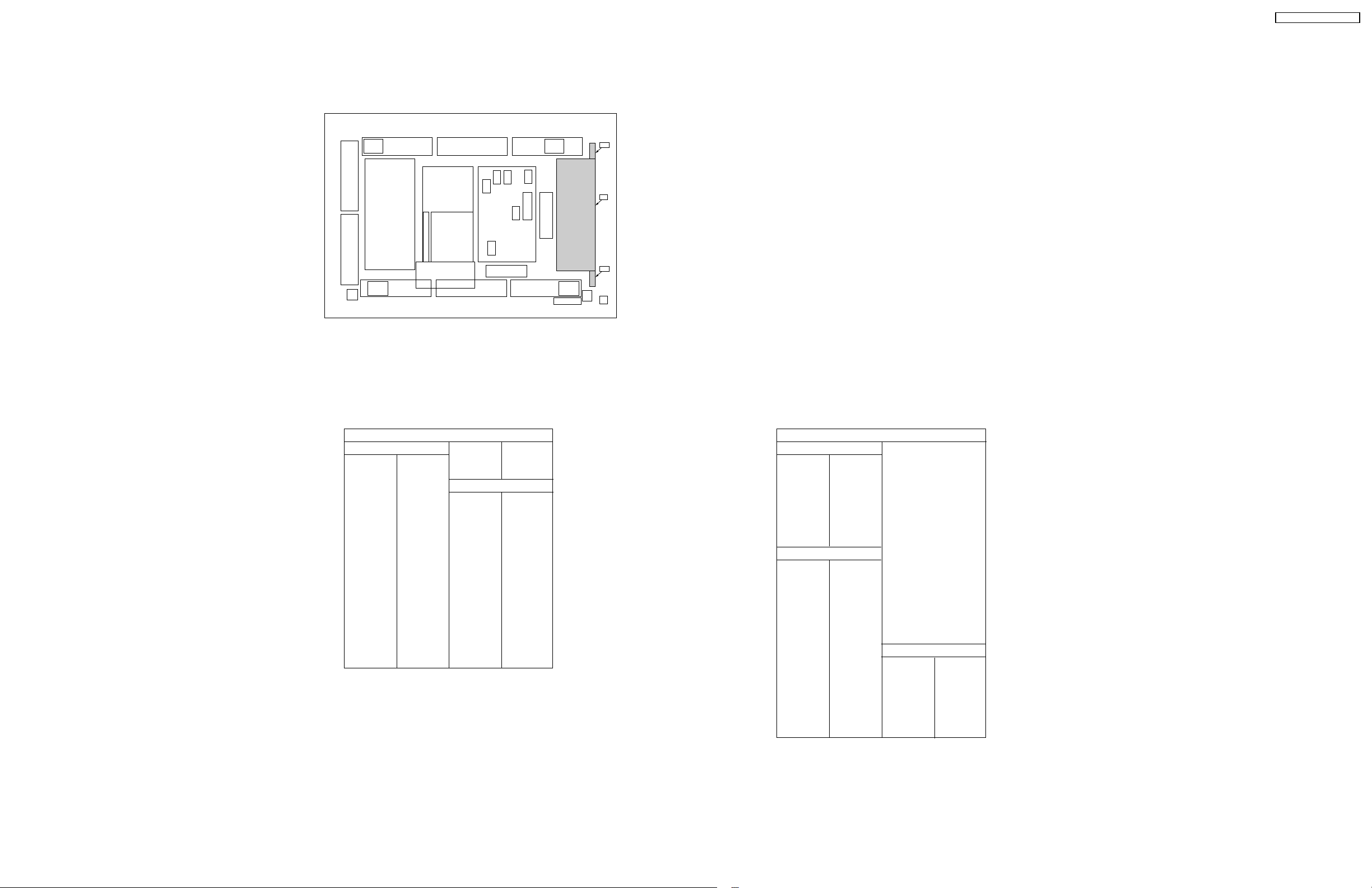
TH-50PHD3 / TH-50PHW3
SS2
SS
SS3
PARTS LOCATION
SS-BOARD (FOIL SIDE)
TRANSISTOR
Q6703 F-3
Q6704 F-3
Q6705 F-3
Q6706 F-3
Q6714 E-3
Q6715 D-3
Q6716 D-3
Q6717 D-3
Q6727 G-5
Q6728 G-5
Q6729 G-5
Q6730 F-5
Q6731 F-5
Q6732 F-5
Q6746 E-5
Q6747 E-5
Q6748 E-5
Q6749 D-5
Q6750 C-5
Q6751 C-5
Q6752 C-5
Q6753 C-5
Q6764 A-5
Q6769 B-5
ADDRESS INFORMATION
Q6777 C-3
Q6778 C-3
Q6779 C-4
Q6783 B-4
TEST POINT
TP1 H-1
TP2 H-1
TP3 H-1
TP4 H-1
TP5 H-1
TP6 G-3
TP7 G-3
TP8 G-3
TP9 G-3
TP10 G-3
TP11 G-3
TP12 H-1
TP13 H-1
TP14 H-1
TP15 H-1
TP17 B-5
TP18 B-5
PARTS LOCATION
SS-BOARD (COMPONENT SIDE)
IC
IC6701 G-3
IC6702 G-4
IC6703 D-4
IC6704 E-4
IC6705 D-5
IC6706 H-4
IC6707 H-4
IC6709 F-3
IC6711 G-4
IC6712 B-3
TRANSISTOR
Q6701 D-3
Q6702 D-3
Q6703 C-3
Q6704 C-3
Q6705 D-3
Q6706 D-3
Q6712 E-3
Q6713 E-3
Q6714 E-3
Q6715 E-3
Q6716 E-3
Q6717 F-3
Q6721 B-5
Q6722 B-5
Q6723 D-5
Q6724 D-5
Q6727 B-5
Q6728 B-5
Q6729 C-5
Q6730 C-5
ADDRESS INFORMATION
Q6731 C-5
Q6732 D-5
Q6740 F-5
Q6741 F-5
Q6744 F-5
Q6746 D-5
Q6747 E-5
Q6748 E-5
Q6749 E-5
Q6750 F-5
Q6751 F-5
Q6752 G-5
Q6753 G-5
Q6761 H-4
Q6762 G-4
Q6763 H-5
Q6764 H-5
Q6765 H-4
Q6766 H-4
Q6777 F-3
Q6778 F-3
Q6779 F-3
Q6783 G-4
TEST POINT
TP15V B-3
TPPR1 B-3
TPSS1 H-5
TPSS2 C-3
TPVe F-3
TPVe2 G-4
TPVSUS A-3
69
Page 70
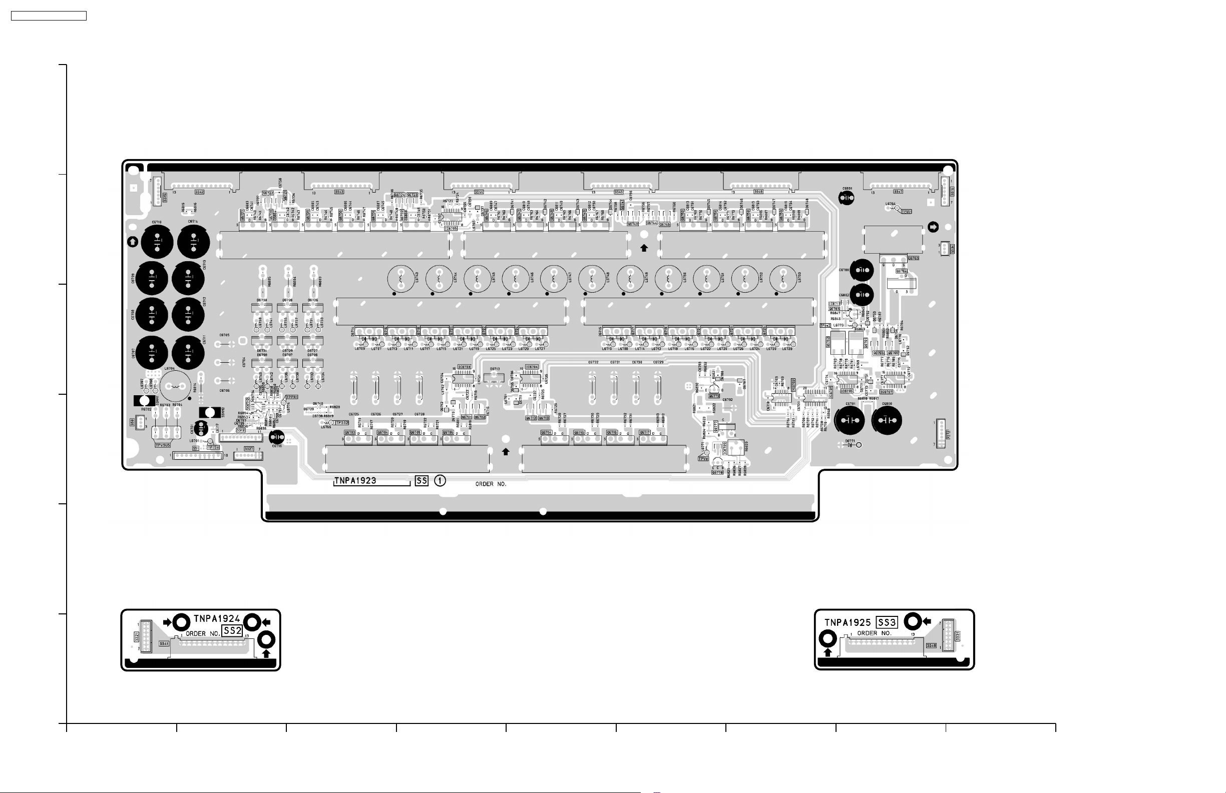
TH-50PHD3 / TH-50PHW3
6
5
SS-BOARD (COMPONENT SIDE)
TNPA1923
4
3
2
SS2-BOARD (COMPONENT SIDE)
TNPA1924
SS3-BOARD (COMPONENT SIDE)
TNPA1925
1
ABCDEFGH I
70
Page 71
13 Block and Schematic Diagrams
13.1. Schematic Diagram Notes
Important Safety Notice
Components identified by mark have special characteristics important for safety.
When replacing any of these components, use only manufacture's specified parts.
Notes:
1. Resistor
All resistors are cabon 1/4W resistor, unless marked as follows:
Unit of resistance is OHM [W] (K=1,000, M=1,000,000).
: Nonflammable : Metal Oxide
: Solid : Metal Film
: Wire Wound : Fuse:
2. Capacitor
All capacitors are ceramic 50V capacitor, unless marked as follows:
Unit of capacitance is mF, unless otherwise noted.
: Temperature Compensation : Electrolytic
: Polyester : Bipolar
M
m T
: Metalized Polyester : Dipped Tantalum
: Polypropylene : Z-Type
3. Coil
Unit of inductance is mF, unless otherwise noted.
4. Test Point
: Test Point position
5. Earth Symbol
: Chassis Earth (Cold) : Line Earth (Hot)
6. Voltage Measurement
Voltage is measured by a DC voltmeter.
Conditions of the measurement are the following:
Power Source ................................................... AC 220V-240V, 50/60Hz
Power Source ...................................................
Power Source ...................................................
Receiving Signal ............................................... Colour Bar signal (RF)
All customer's controls ...................................... Maximum positions
7. Number in red circle indicates waveform nember.
(See waveform pattern table.)
8. When arrow mark ( ) is found, connection is easily found from the direction of arrow
NP
+
-
Z
(A, B and E Version)
AC 120V, 50/60Hz (U Version)
TH-50PHD3 / TH-50PHW3
Remarks:
1. The Power Circuit contains a circuit area which uses a separate power supply to isolate the
earth connection.
The circuit is defined by HOT and COLD indications in the schematic diagram. Take the
follwing precautions.
All circuits, except the Power Circuit, are cold.
Precautions
a. Do not touch the hot part or the hot and cold parts at the same time or you may
be shocked.
b. Do not short- circuit the hot and cold circuits or a fuse may blow and parts may
break.
c. Do not connect an instrument, such as an oscilloscope, to the hot and cold
circuits simultaneously or a fuse may blow.
Connect the earth of instruments to the earth connection of the circuit being
measured.
d. Make sure to disconnect the power plug before removing the chassis.
2. Following diodes are interchangeable.
MA150- MA162 (Replacement part)
9. Indicates the major signal flow. : Video Audio
10. This schematic diagram is the latest at the time of printing and subject to change without
71
Page 72
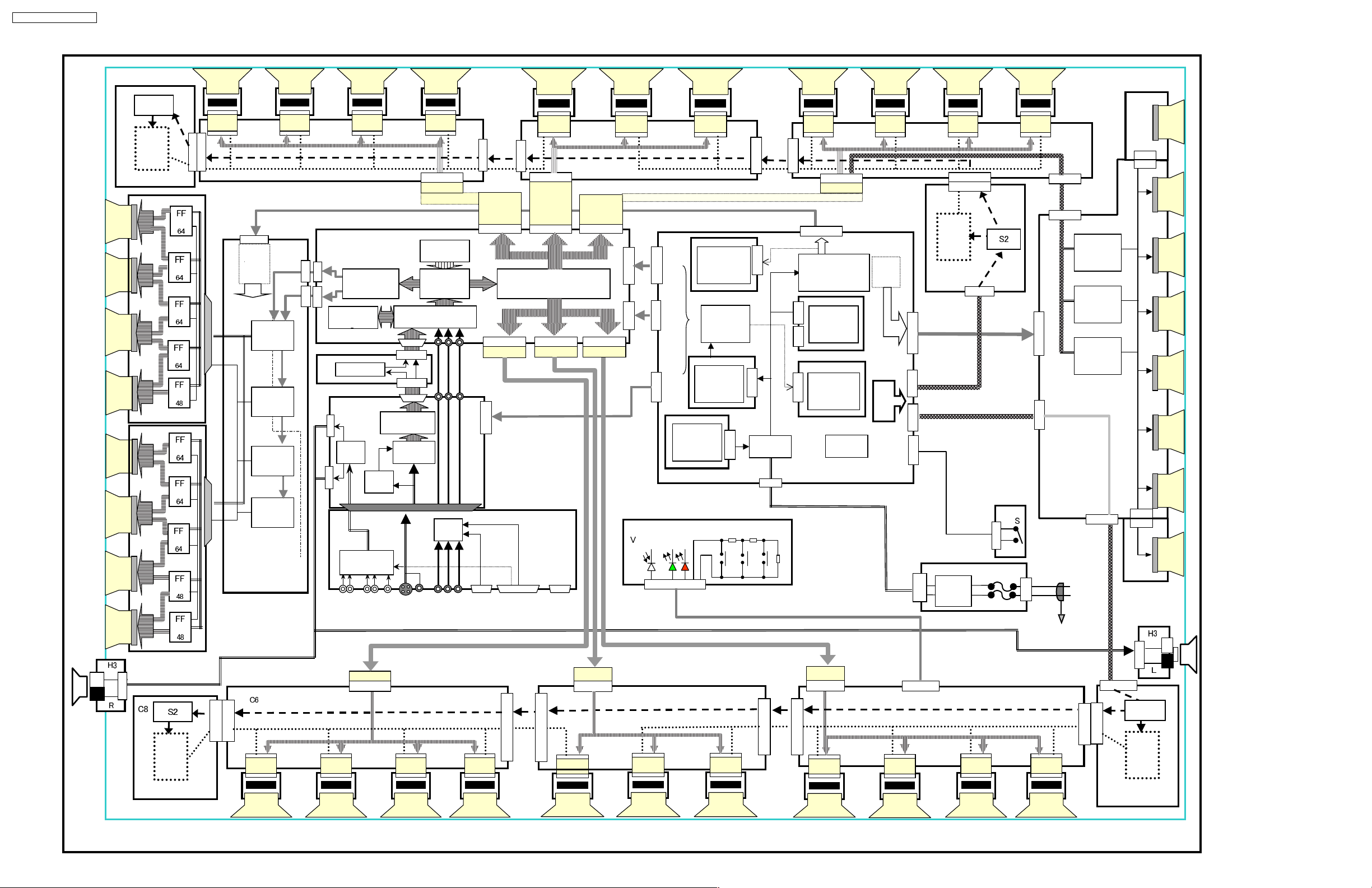
AI
C
SS.R.
(VE)
gy
gy
gy
TH-50PHD3 / TH-50PHW3
13.2. Main Block Diagram
C8
S2
S1
S3
Energy recover
SD
VDA
75V
SS.R. SS.R. SS.R. SS.R.
C12
C81
C1
VDA 75V
78V
SU
SC1
SC
VSUS
VSET
VDA
CONTROL
PULSE
SUSTAIN
PULSE
INITIALIZE
PULSE
SC2
SC3
D
D20
D21
FORMAT
CONVERTE
T11
Digital Buffer
DG
DG5
AUDIO
DG4
DISCHARGE
CONTROL
DIGITAL
YC PROCESS
AMP
NTSC
3D-YC
C11
MICRO
PLASMA
I/P CONV.
RGB PROCESSOR
T2
T1
RGB
VIDEO
A/D
VDA
C13
75V78V
78V
D31
D36 D35
DG6
SS.R. SS.R. SS.R.
C2
C22
VDA 75V
C21
D32
SUB-FIELD
PROCESSOR
D33
D5 D7
D34
78V
P5
P7
P6
P
13.5V
5V
3.65V
OFF
SOS
STB5V
+15V
-15V
MUTE
P6
P7
SUSTAIN
VOLT AGE
PROTECT OR
PROCESS
VOLT AGE
RECTIFIER
P5
PROCESS
VOLT AGE
CONTROL
POWER
FACTOR
CONTROL
Vda
P19
VDA
C23
75V
78V
P21
P18
PRIMARY
CIRCUIT
P9
SS.R. SS.R. SS.R. SS.R.
C33
78V
S1
C35
C71
VDA
75V
C35
P2
S3
SUSTAIN
VOLT AGE
RECTIFIER
SUSTAIN
P15P16
VOLT AGE
CONTROL
PROCESS
VOLT AGE
P22
PROTECT OR
STAND BY
VSUS
VSET
VDA
P3
P8
Ener
Recover
C72
P1
P26
VDA
75V
P27
P8
C7
SS1
SS27
C3
SS12
SS12
VDA 75V
SS41
SS15
Vda
SS
ADDRESS
VOLT AGE
SUSTAIN
PULSE
ERASE
PULSE
SCAN
VOLT AGE
FLOATING
GROUND
from DG5
SPEAKER
+
TERMINAL
AUDIO SW
AV RGB PC
AUDIO IN
C61
AV /
S-VIDEO
RGB
SW
RGB/
COMPONENT
P
-
VDA 75V
78V
C63
S1
C81
C62
C52
C5
H
POWER
SWITCH
AC100V
- 240V
F1
from DG4
C51
REMOTE
RECEIVE
VDA 75V
78V
POWE
V34
Vda
R
F
LINE
C44
F2
FILTER
VDA 75V
78V
INPUT
-
+
C41
C4
C53
C43
Vda
SS8
C42
SS72
C71
S3
Ener
recover
SS.R. SS.R. SS.R.
SS
SS.R. SS.R.
SS
SS.R.
SS.R. SS.R.
C72
75V
78V
Ener
SS16
SS48
SPEAKER
TERMINAL
+
-
C7
S2
S1
S3
recover
72
Page 73
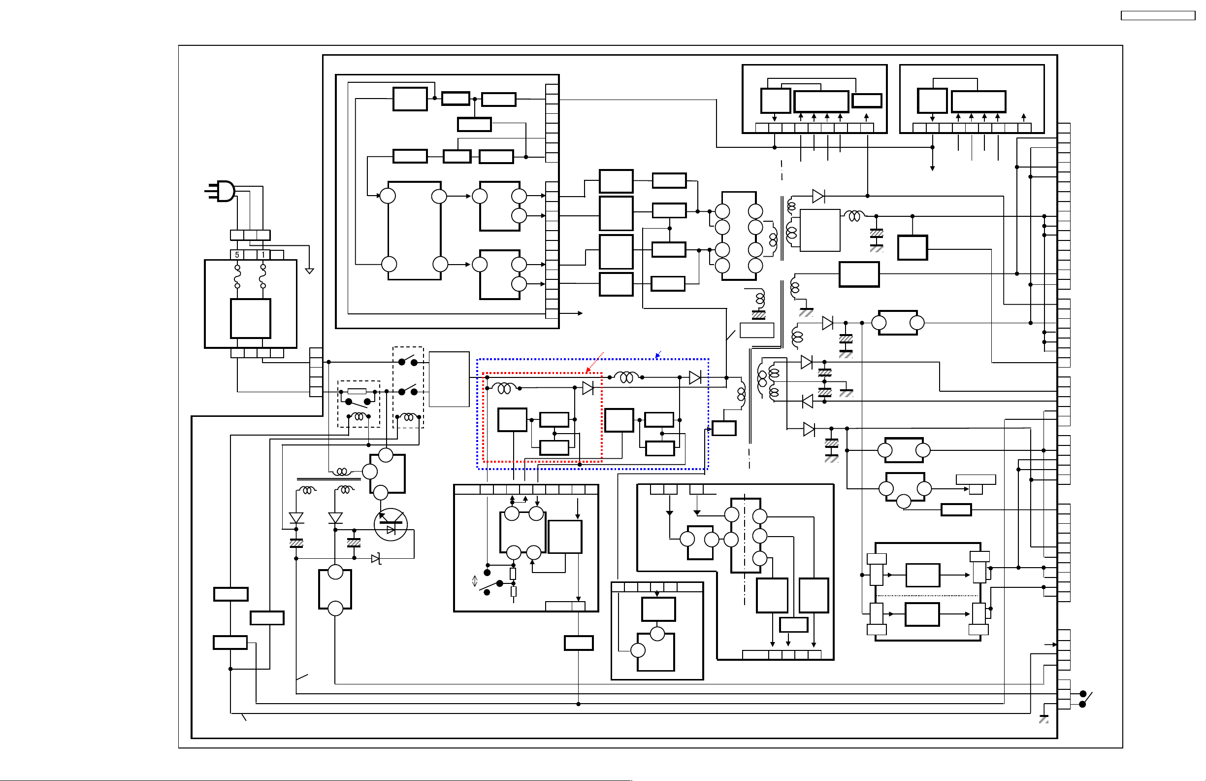
13.3. Power (F, P1, P3, P4, P5, P6, P7, P8 and P9 Board) Block Diagram
D601
D604
Q636
IC635
Q601
AC
IN VBK VDA 15Vs 13.5V
D606
Q635
AC INLET IC601 IC602 SOS
3
14
6 4
L4
2
H6 2 VSUS
OSC. 4
IC600
F1
8
11
26
H8
F901 F900 9VDA
4
L10 10 15V
P3
LINE 13 STOP
FILTER 6 15V
F
RL401 D402 3
15F9
Q417
Q418
Q421
ON/OFF From MICRO
P9 POWER FACTOR CONTROL 4
3 5 VBK
RL400
1 1 +15V
3
IC400
1
2
D431
T402
3
D439D440
FULL
WAVE
RECTIFIER
L401 D407
Q419
Q400
P19 8 4 5 7 11
7
IC735
+
+
55V
1 13.5V
1
IC403
AVR
5
9 3.65V
230V
110V
12
PFC
3
STB 5V
MAIN POWER SWITCH ON/OFF
P16
SOS IN
1 VCC
6FB
8 VSUS VSUS 15V VSET -15Vs 5V
P15
G
G
D
Q404
S
Q405
D
STOP
FAN
OCP
4
IC737
IC736
Q730
5
PROTECT
P6
P19 9
D430
DRIVE VOLTAGE PROTECT OR PROCESS VOL TAGE PROTECTOR
Q750
Q751
IC750
COMPARATO
P7
IC751
Q775
Q776
IC775
COMPARATO
P8
P21
10 4367 1
P22
7 4321 6
P26
2VDA
5 15V
P27
Q408
Q409
Q402
T404
Q410
Q403
T405
Q411
Q406
Q407
230V_Model
Q425
Q401
5 1 P18 11 3.65V
GD
Q414
Q412
Q413
Q415
G
110V_Model
L402
G
Q423
S
Q424
G
P42
Start
STOP
Q650
Q651
PROTECT
6
8
IC650
OSC.
S
D
D
S
D
D432
D
D
7
P41
DC400V
6
31
OSC.
IC921
P5
2
3
9
10
Vcc
Q416
L411
T400
5
6
12
13
T401
D487
FULL
WAVE
RECTIFIER
L434
IC406
R528
+
IC410
R513
VDA75V
VBK
D444
DC400V
2 VSUS
+
D441
+
3 -15V
75V
+
D442
IC412
1 2
AVR
+15V
For Audio
-15V
4 MUTE
D443
P10-P13
12
11
10
Q932
Q933
IC931
Vscan
F15V
Vad
Q926
Q927
IC934
3
5
T921
IC932
+
IC407
1 2
AVR
IC411
1 2
P29
1
25v 3.65v
2
1
25v 3.65v
2
P30
P4
P43
6 5 4 2 ON/OFF
15V
13.5V
5V
55V
12V
1To
AVR
4
Q429
P9_1
IC981
IC981
P9_2
P29
5
6
5
6
P30
1VDA
5 15V
P1
3
1 VSET
P2
P6
P17
8 3.65V
9 3.65V
1 13.5V
P5
8
P7
7 SOS
4 STB5V
P8
1
2
TH-50PHD3 / TH-50PHW3
To C72
To SS1
To SC1
To DG6
To DG17
FAN
To D5
To D7
To SS8
MAIN
SWITCH
73
Page 74
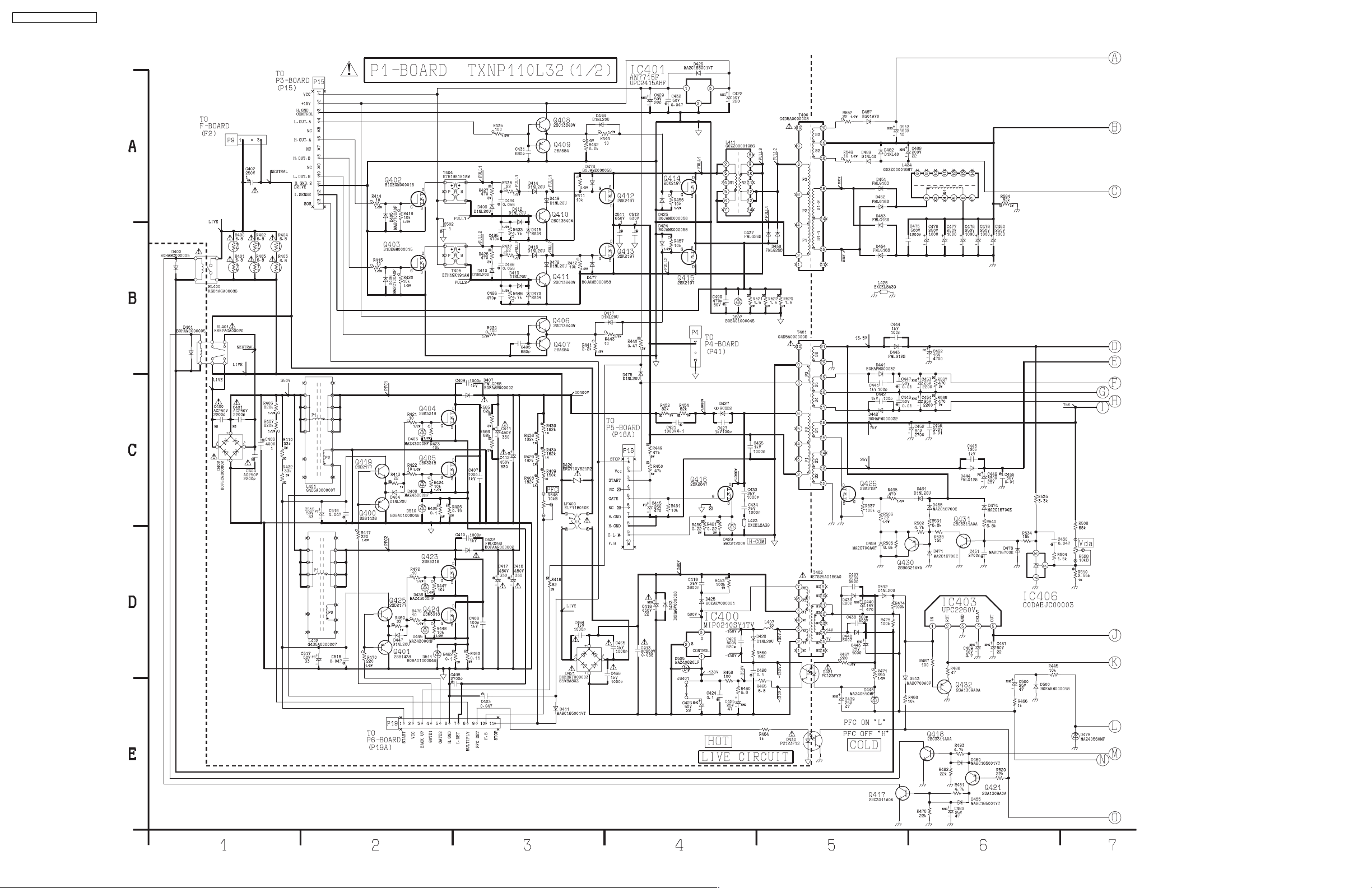
TH-50PHD3 / TH-50PHW3
13.4. P1-Board (1/2) Schematic Diagram
74
Page 75
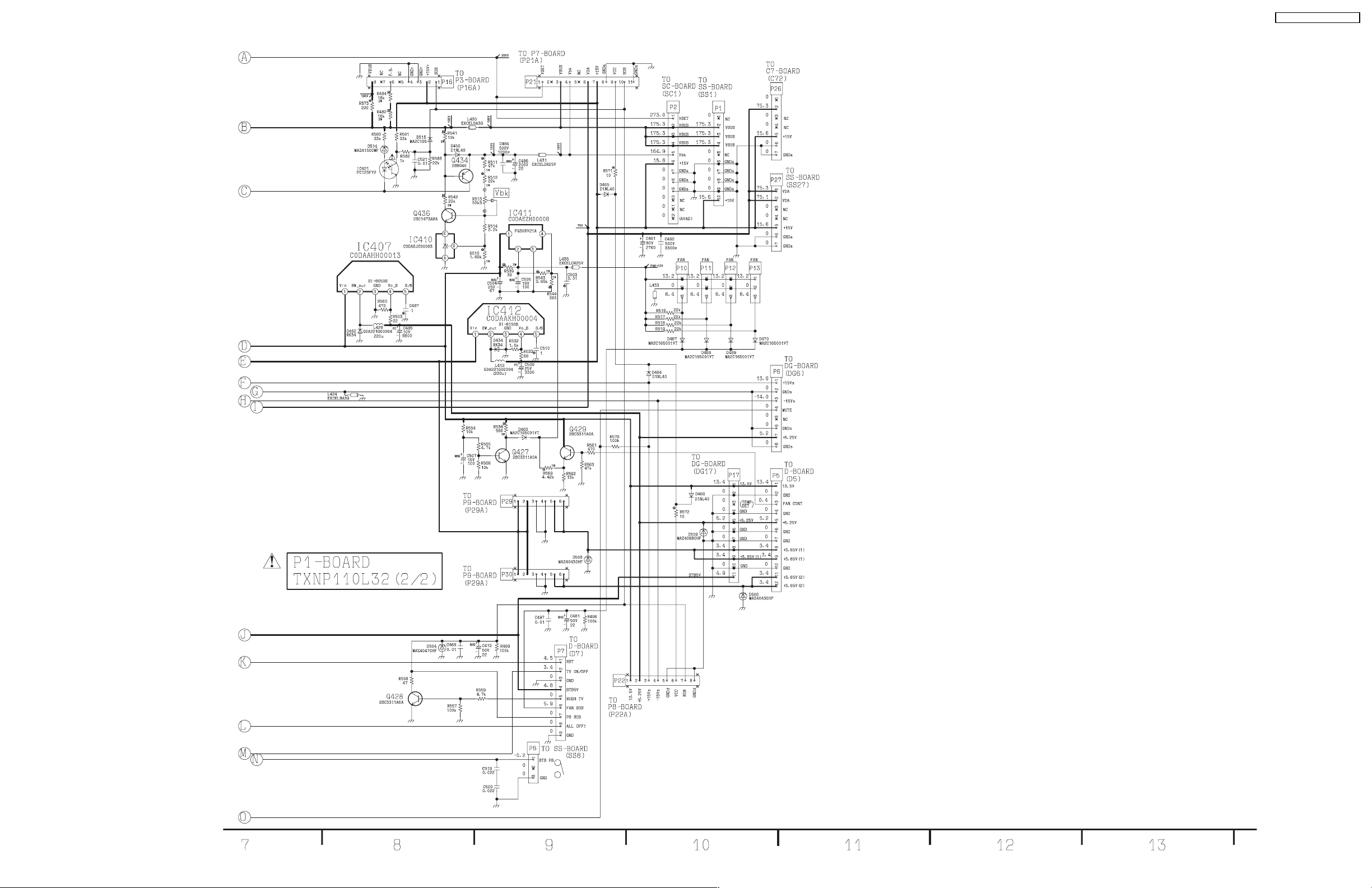
13.5. P1-Board (2/2) Schematic Diagram
TH-50PHD3 / TH-50PHW3
75
Page 76
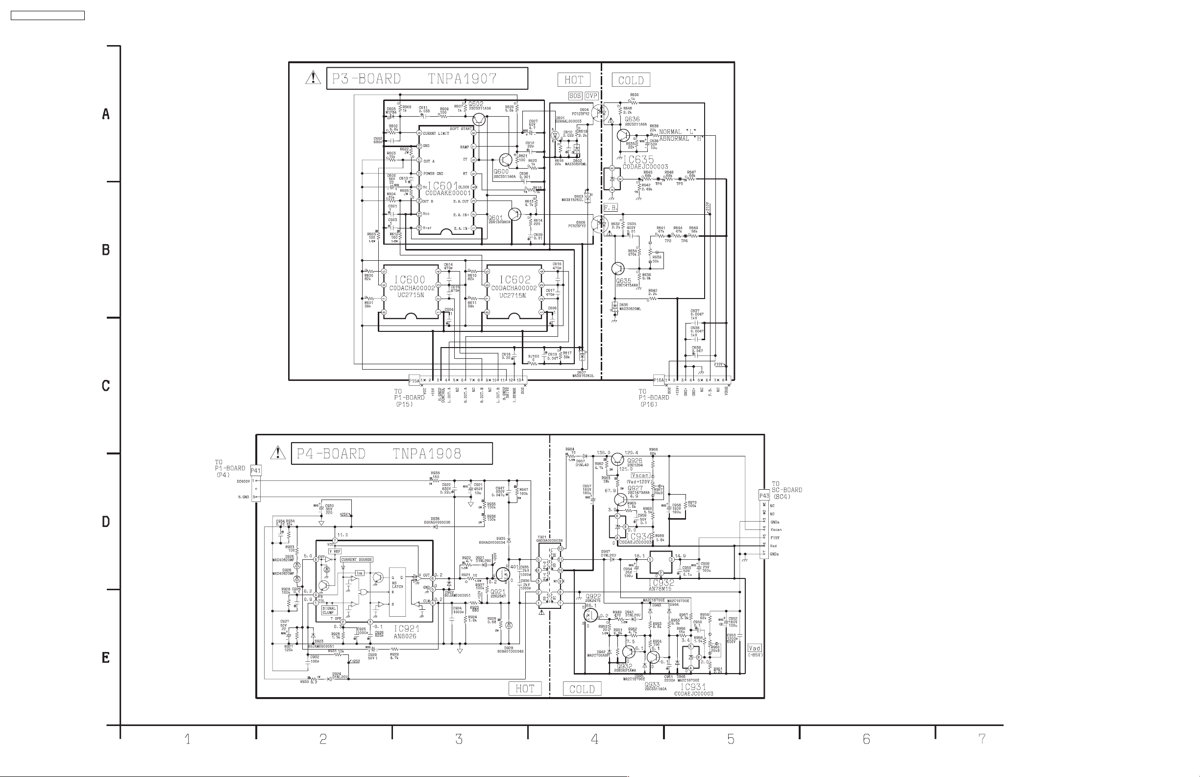
TH-50PHD3 / TH-50PHW3
13.6. P3 and P4-Board Schematic Diagram
76
Page 77
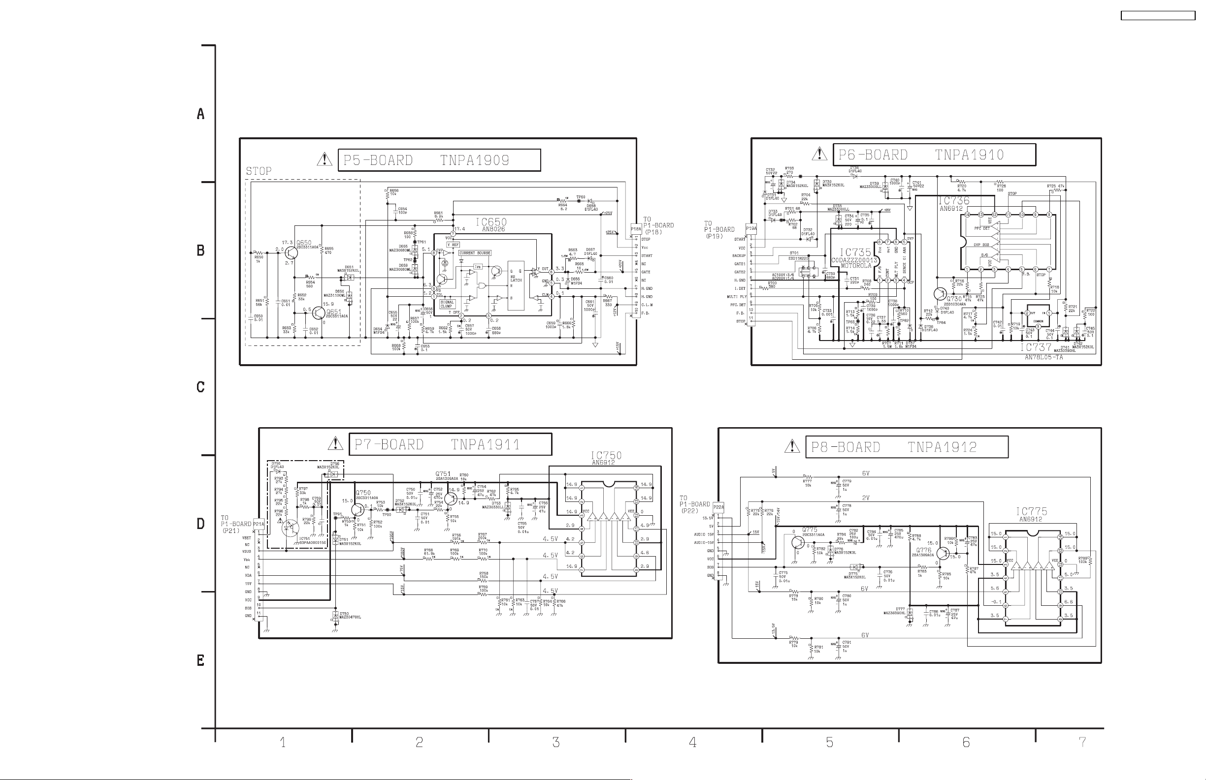
13.7. P5, P6, P7 and P8-Board Schematic Diagram
TH-50PHD3 / TH-50PHW3
77
Page 78
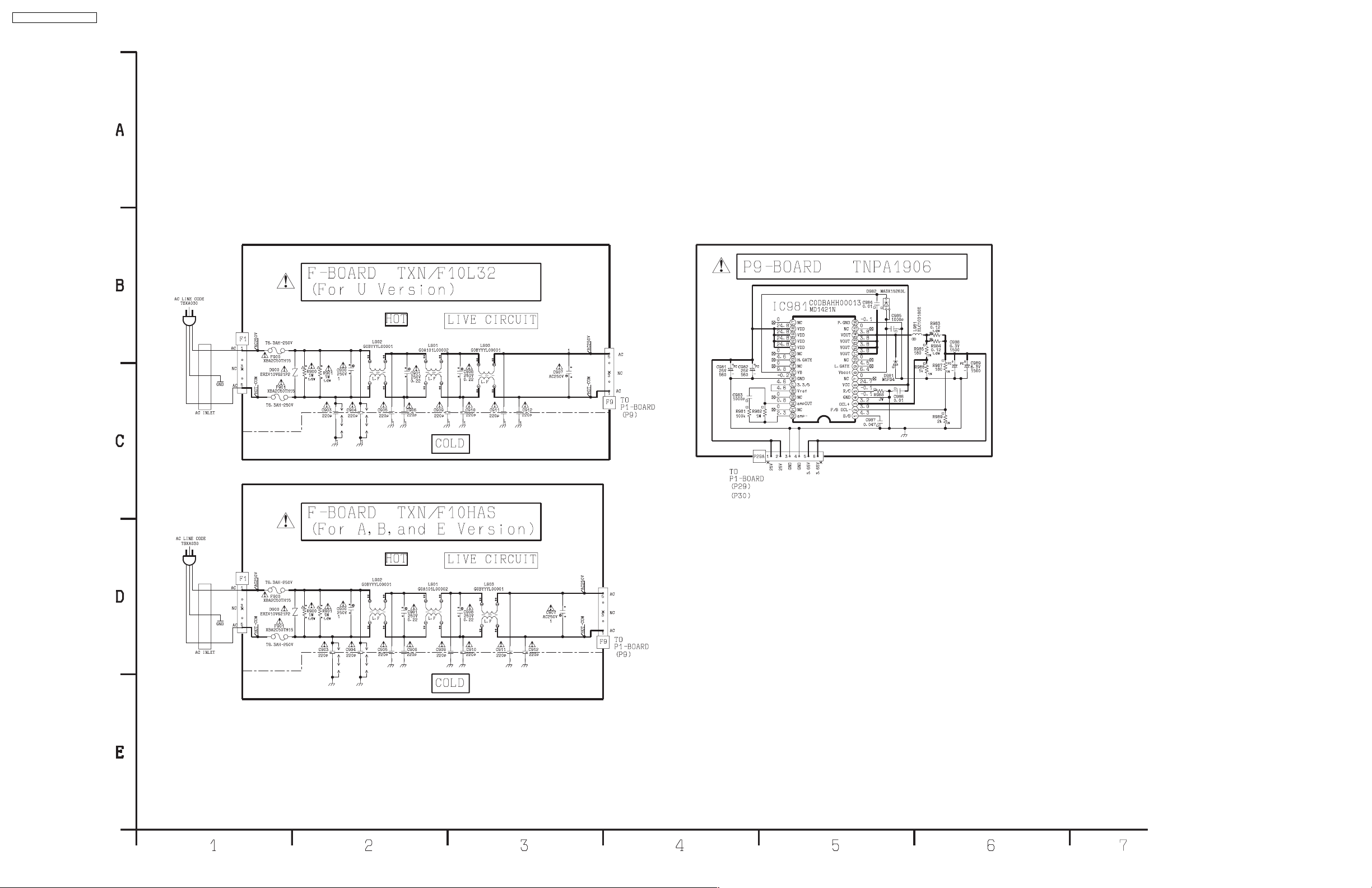
TH-50PHD3 / TH-50PHW3
13.8. P9 and F-Board Schematic Diagram
78
Page 79
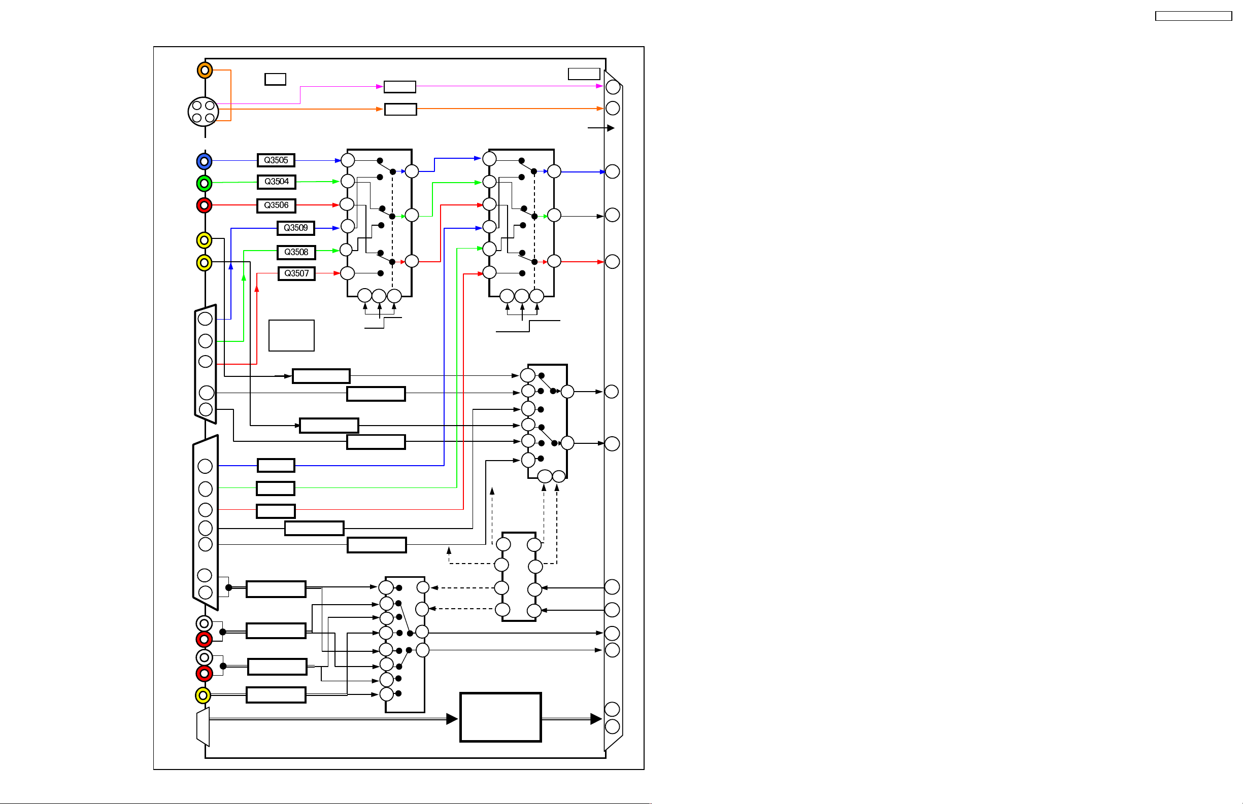
13.9. H-Board Block Diagram
VIDEO
IN C
S-VIDEO
IN VIDEO/Y
COMPONENT/RGB IN RGB - PC SEL. RGB/PC - TUNER SEL.
Pb/B Pb/B
Y/G Y/G
H
Q3503
Q3501
IC3505 IC3508
8
6
11
8
11
JK3501
TO DG BOARD
Pb/B
6
TH-50PHD3 / TH-50PHW3
5
1
11
Pr/R Pr/R
HD
VD Pr/R
PC IN
B
3
G
2
R SYNC.SEL.
1
DDC
MEMORY
Q3517/Q3518
13
HS
VS
14
Q3519/Q3514
TUNER VD
IN
B
2
G DAC3
1
R
3
4
HD
VD
5
AUDIO
7
8
R0
AV
L0
Q3525/Q3526
L1
Q3527/Q3528
Q3512
Q3511
Q3510
Q3521/Q3522
R1
RGB/
COMP.
L2
Q3529/Q3530
R2
L3
PC
Q3531/Q3532
R3 SCL1
RS232C
16
5
9
14
3
1
2
7 12
16
B
9
G
14
R
1
RGB PC
DAC2 DAC3 IC3504
Q3513/Q3514
Q3513/Q3514
Q3523/Q3524
IC3506
DAC2
AUDIO SEL.
1
5
2
4
12
14
15
11
9
10
LDAC0
3
13
DAC1
RR
REMOTE
INTERFACE
BLOCK
2 7 12
RGB&PC TUNER
15
11
12
2
4
1
10
SW3 SW2
IC3507
CONTROL
4
5
6
7
IIC
DAC
9
10
|
15
14
5
3
HD HD
13
VD
3
9
SDA1
Y/G
SCL3
SDA3
L
9
7
37
39
56
57
31
33
52
53
IC3503, IC3511 ~ 14
79
Page 80
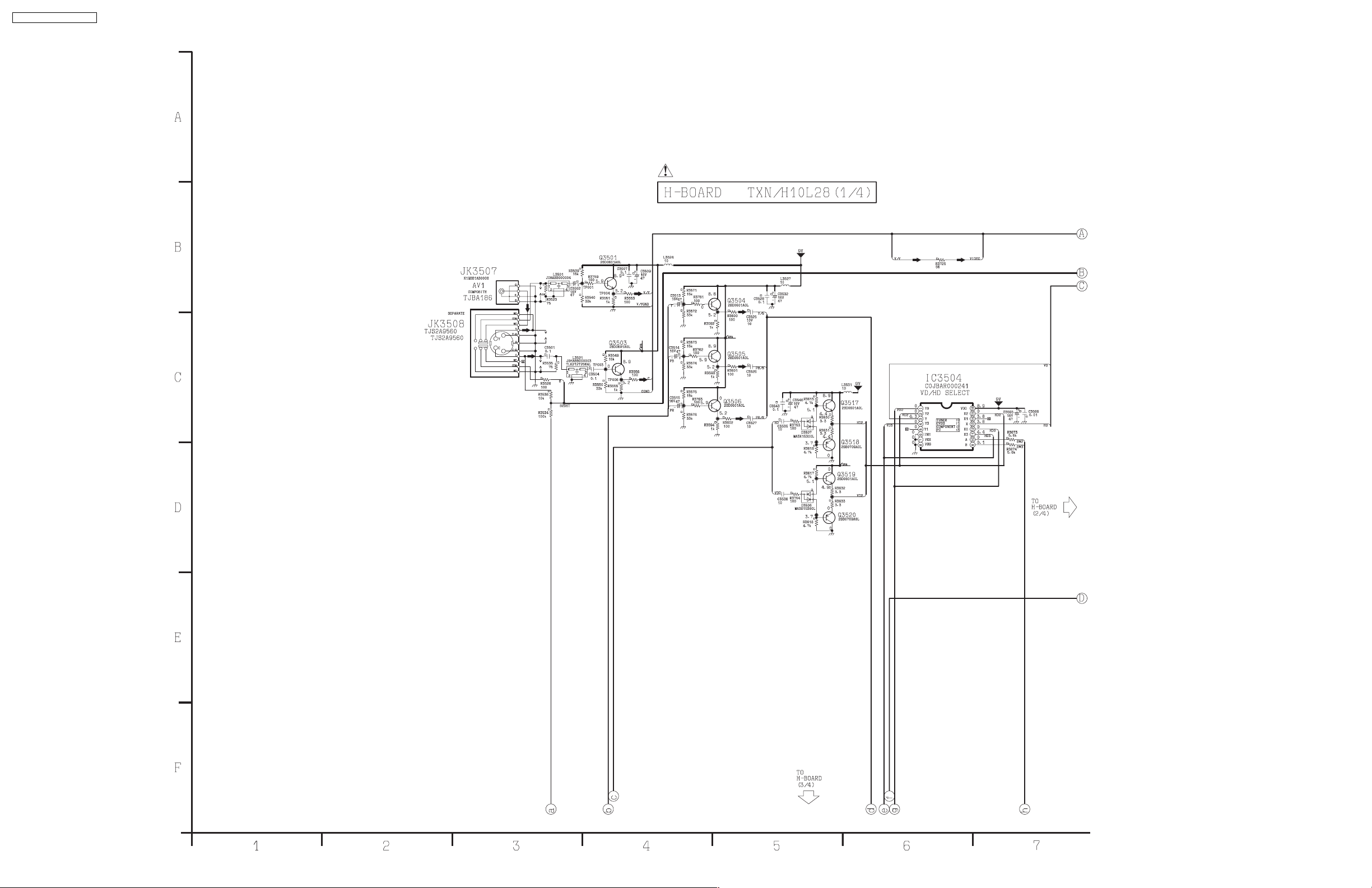
TH-50PHD3 / TH-50PHW3
13.10. H-Board (1/4) Schematic Diagram
80
Page 81
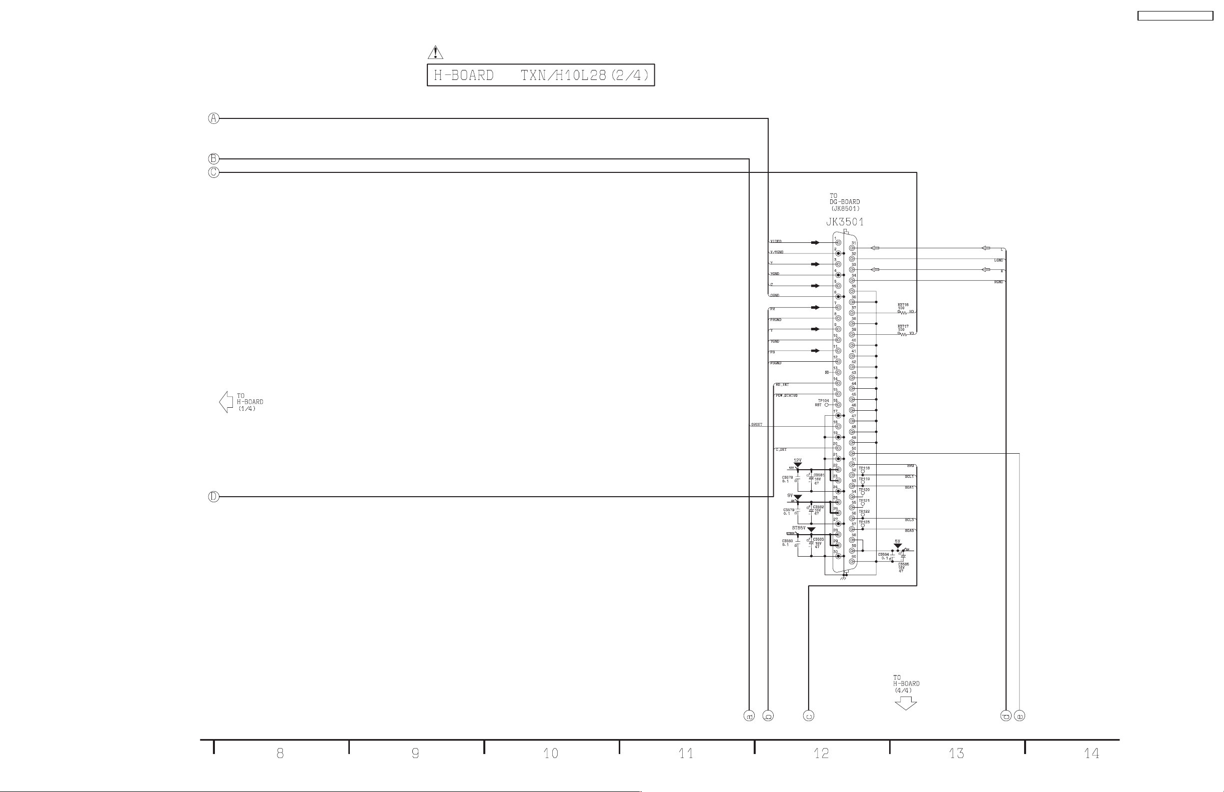
13.11. H-Board (2/4) Schematic Diagram
TH-50PHD3 / TH-50PHW3
81
Page 82
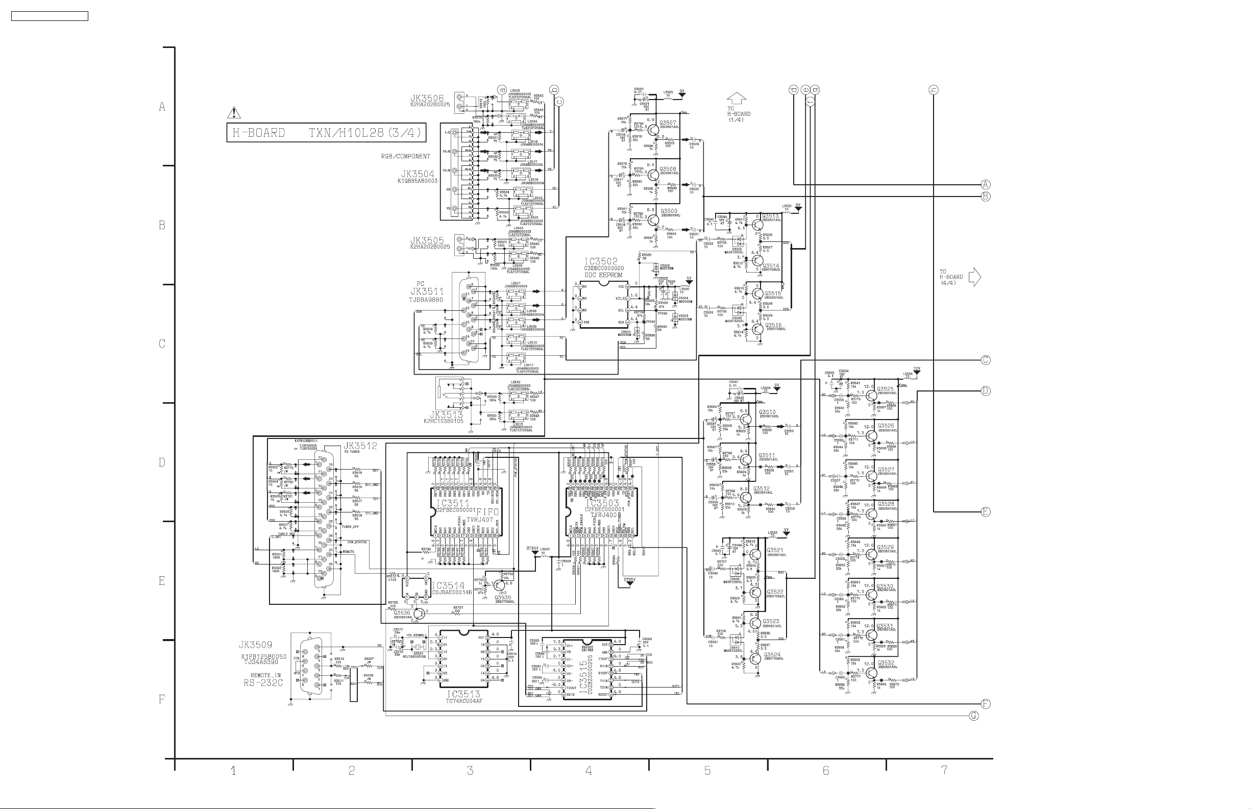
TH-50PHD3 / TH-50PHW3
13.12. H-Board (3/4) Schematic Diagram
82
Page 83
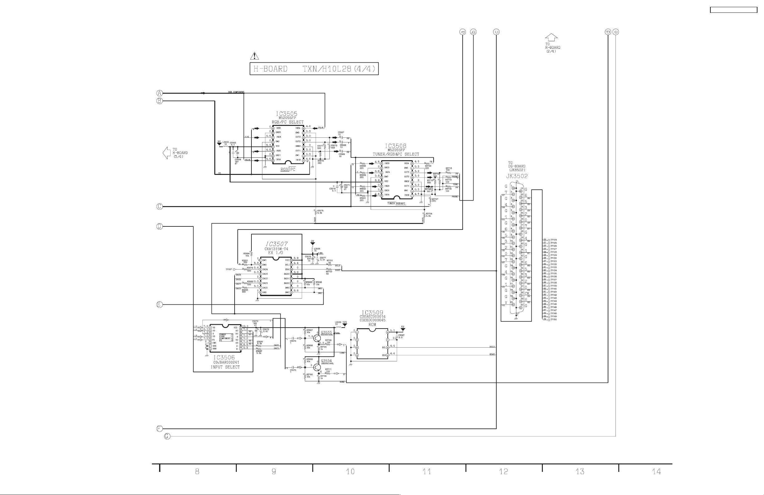
13.13. H-Board (4/4) Schematic Diagram
TH-50PHD3 / TH-50PHW3
83
Page 84
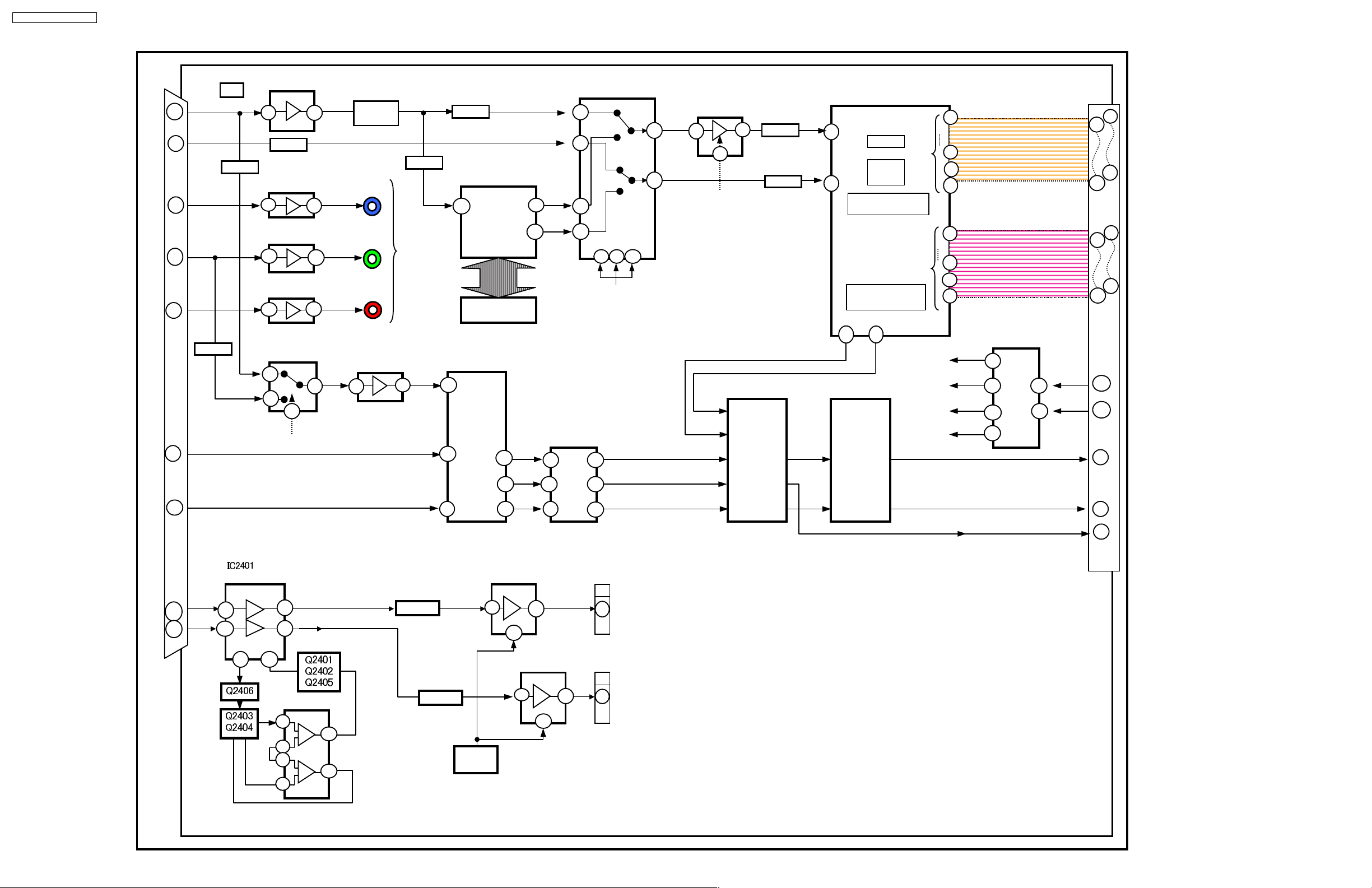
TH-50PHD3 / TH-50PHW3
13.14. DG Board Block Diagram
DG
V/Y V/Y IC8018
1
C SC
5
Q8005
IC8001
3
Q8001
1
Q8007
/LC8002
Q8006
Q8014
IC8007 C 0
IC8003 JK8003
PB Y Sub Contrast
11
3
1
88
NTSC
3D YC
84
COMB
IC8002 JK8002
Y
9
3
1
To
D-Board
FILTER
83
IC8004 JK8001
PR
7
3
1
4M DRAM
FIELD MEMORY
IC8014
1
3
14
5
16
C
11
2 7 12
IC8015
Y 7
1
3
Q8032
2
Q8031
L : 3D YC
IC8008
Q8021
HD H:G Sync
37
VD
39
IC8005 IC8020
RGB SYNC.SEL CLP VS L:3DYC
7
1
6
5
IC8009
1
3
IC8010
4
6
8
SYNC
SEP.
IC8016 & Q8030 IC8033 & Q8033
IC8011
SYNC.
HD- HP H HD
15
17
13
1
CLP NCLP CLP
9
VD VP V VD
1
SYNC
10
8
2
AV/
RGB/COMP
.
SYNC. SW
62
63
DIGITAL
BUFFER
VPC
A/D
COMB
FILTER
COLOUR
DECODER
SYNC.
PROCESS
1216
20
Y2
25
1
28
29
38
7
43
C2
1
46
0
47
4
L:VPC SCL3
L:DIGITAL SDA3
H:G Sync
IIC
5
14
|
SW
7
9
15
D-Board
CLP
To
33
41
30
38
25
46
28
43
13
58
6
8
4
AUDIO AMP IC2302
L
L TO SPEAKER
31
33
32
1
R
29
28
20
12
Q2301
11
4
12
IC2301
L
IC2402
6
5
3
2
Q2302
7
MUTE
11
Q2303
1
Q2304
4
12
DG4
DG5
1
TO SPEAKER
1
84
Page 85
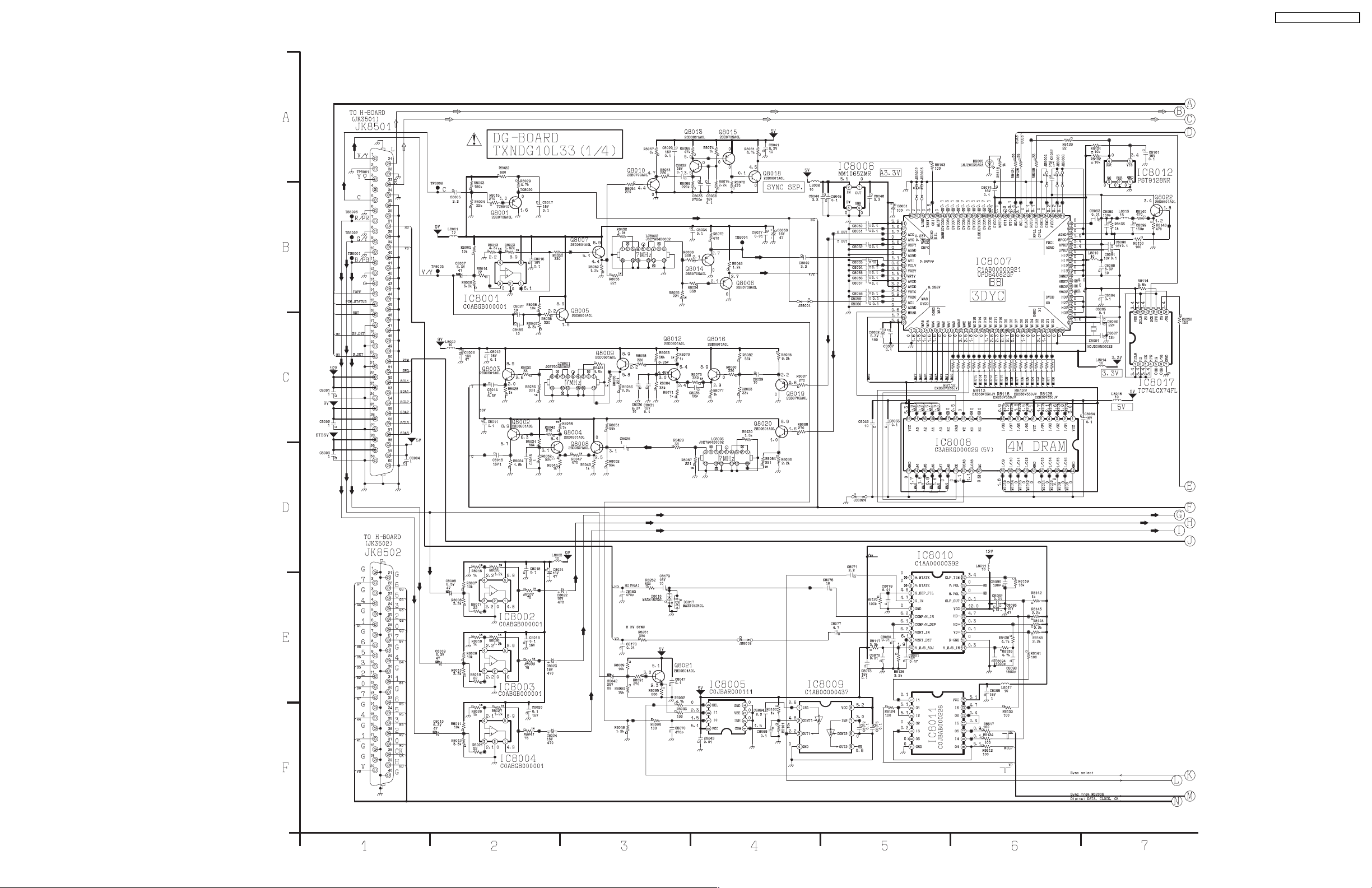
13.15. DG-Board (1/4) Schematic Diagram
TH-50PHD3 / TH-50PHW3
85
Page 86
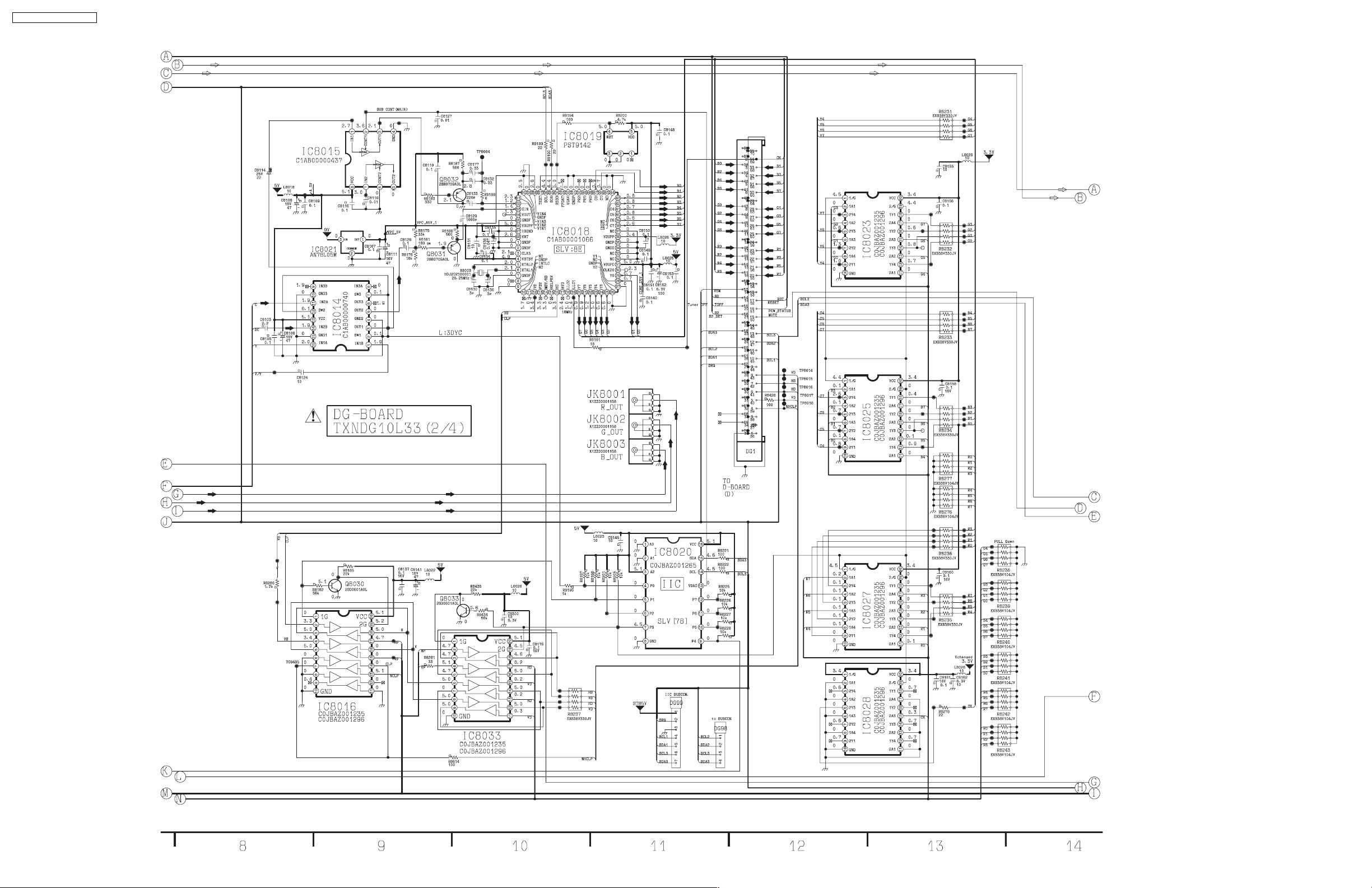
TH-50PHD3 / TH-50PHW3
13.16. DG-Board (2/4) Schematic Diagram
86
Page 87
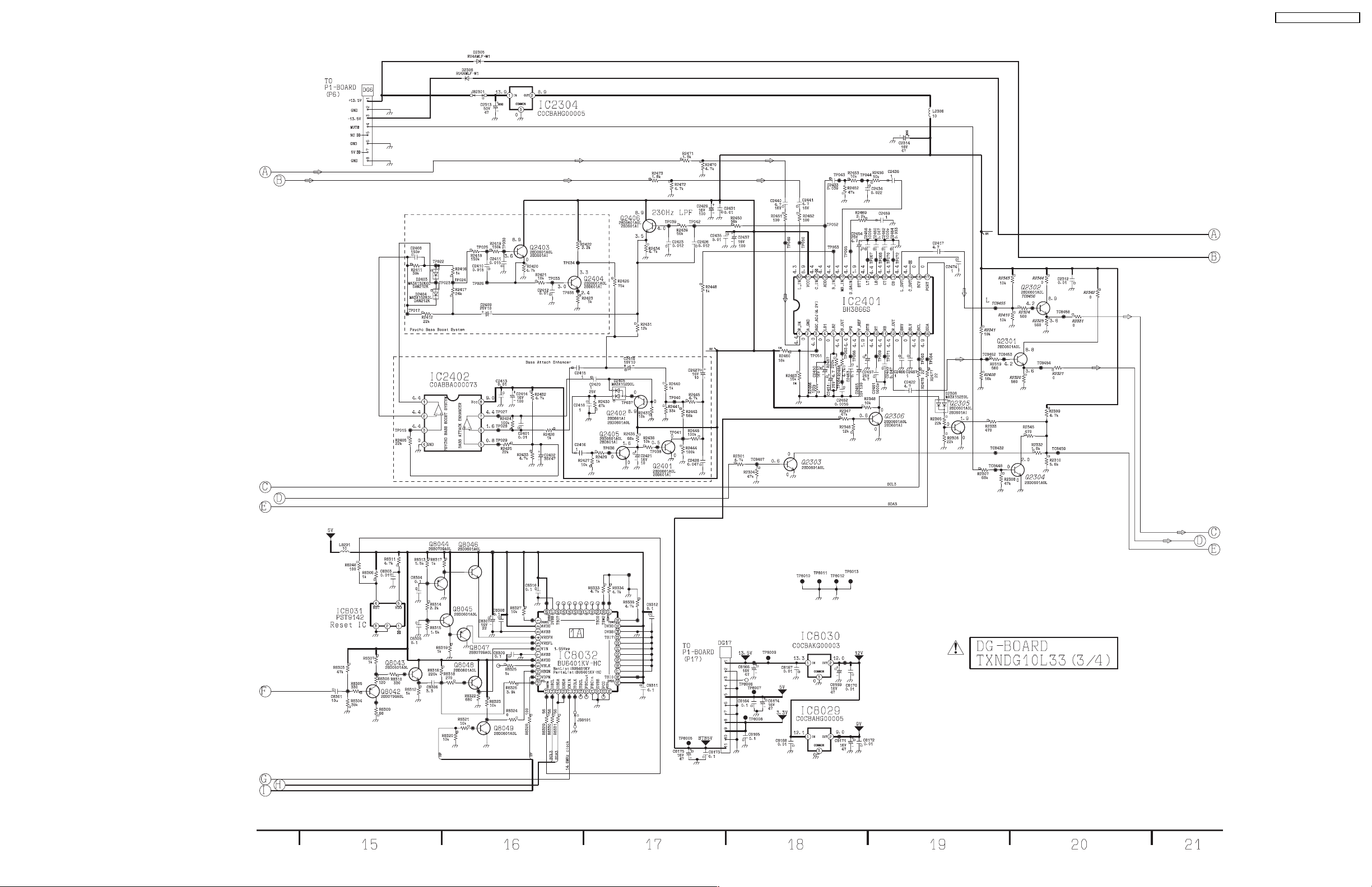
13.17. DG-Board (3/4) Schematic Diagram
TH-50PHD3 / TH-50PHW3
87
Page 88
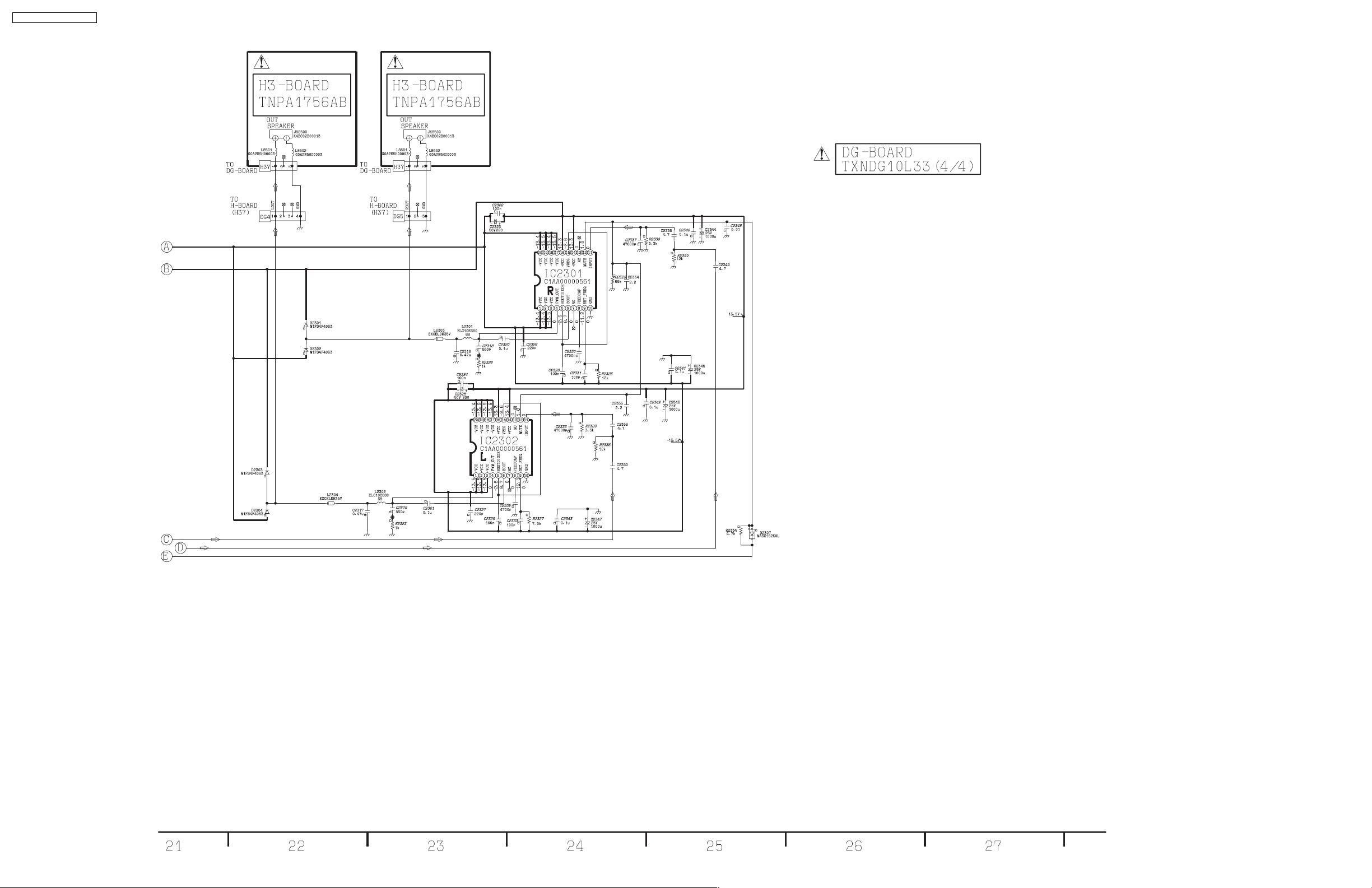
TH-50PHD3 / TH-50PHW3
13.18. DG-Board (4/4) Schematic Diagram
88
Page 89
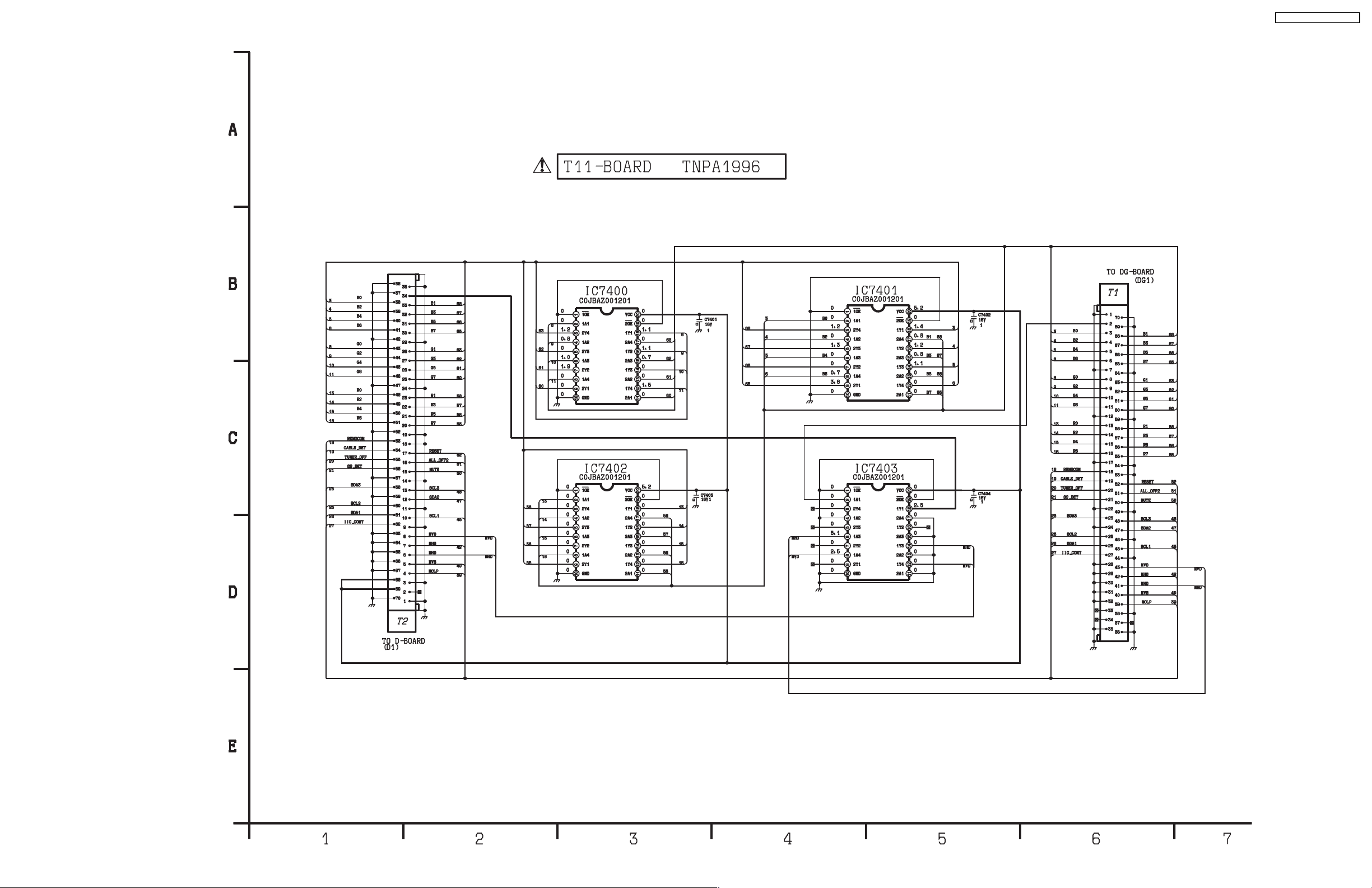
13.19. T11 Board Schematic Diagram
TH-50PHD3 / TH-50PHW3
89
Page 90
TH-50PHD3 / TH-50PHW3
13.20. D-Board IC Location
IC No. */36 Page IC No. */36 Page
IC9000 1 95 IC9502 23 117
IC9001 1 95 IC9503 10 104
IC9002 13 107 IC9504 11 105
IC9003 1 95 IC9505 35 129
IC9004 1 95 IC9506 34 128
IC9005 1 95 IC9507 23 117
IC9006 13 107 IC9508 23 117
IC9007 2 96 IC9509 23 117
IC9008 2 96 IC9510 23 117
IC9009 2 96 IC9511 23 117
IC9010 1 95 IC9512 24 118
IC9012 13 107 IC9513 24 118
IC9014 4 98 IC9516 21 115
IC9015 25 119 IC9520 10 104
IC9016 25 119 IC9521 34 128
IC9017 25 119 IC9551 19 113
IC9018 2 96 IC9552 8 102
IC9019 1 95 IC9554 8 102
IC9020 1 95 IC9555 32 126
IC9021 1 95 IC9557 20 114
IC9022 1 95 IC9558 8 102
IC9023 1 95 IC9559 20 114
IC9024 28 122 IC9560 8 102
IC9036 16 110 IC9561 20 114
IC9047 5 99 IC9562 21 115
IC9048 29 123 IC9563 21 115
IC9061 7 101 IC9564 21 115
IC9093 4 98 IC9565 21 115
IC9200 3 97 IC9701 26 120
IC9201 3 97 IC9702 26 120
IC9202 3 97 IC9703 26 120
IC9204 4 98 IC9704 27 121
IC9206 16 110 IC9705 27 121
IC9207 4 98 IC9706 26 120
IC9209 4 98 IC9707 27 121
IC9210 16 110 IC9900 2 96
IC9211 4 98 IC9901 3 97
IC9211 4 98 IC9902 3 97
IC9212 4 98 IC9903 3 97
IC9213 4 98 IC9904 3 97
IC9214 4 98 IC9905 3 97
IC9215 4 98 IC9906 3 97
IC9217 4 98 IC9907 3 97
IC9223 15 109 IC9908 2 96
IC9225 5 99 IC9909 2 96
IC9226 29 123
IC9250 27 121
IC9251 27 121
IC9254 28 122
IC9259 28 122
IC9302 5 99
IC9352 29 123
IC9400 6 100
IC9401 6 100
IC9401 6 100
IC9402 6 100
IC9403 6 100
IC9450 30 124
IC9451 30 124
IC9452 30 124
IC9453 30 124
IC9501 22 116
90
Page 91
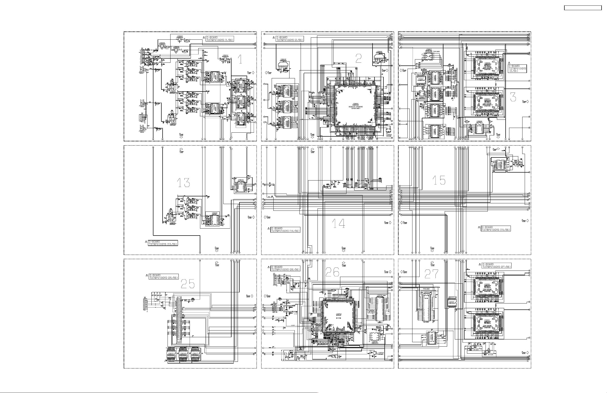
13.21. D-Board Information (1/4)
TH-50PHD3 / TH-50PHW3
91
Page 92
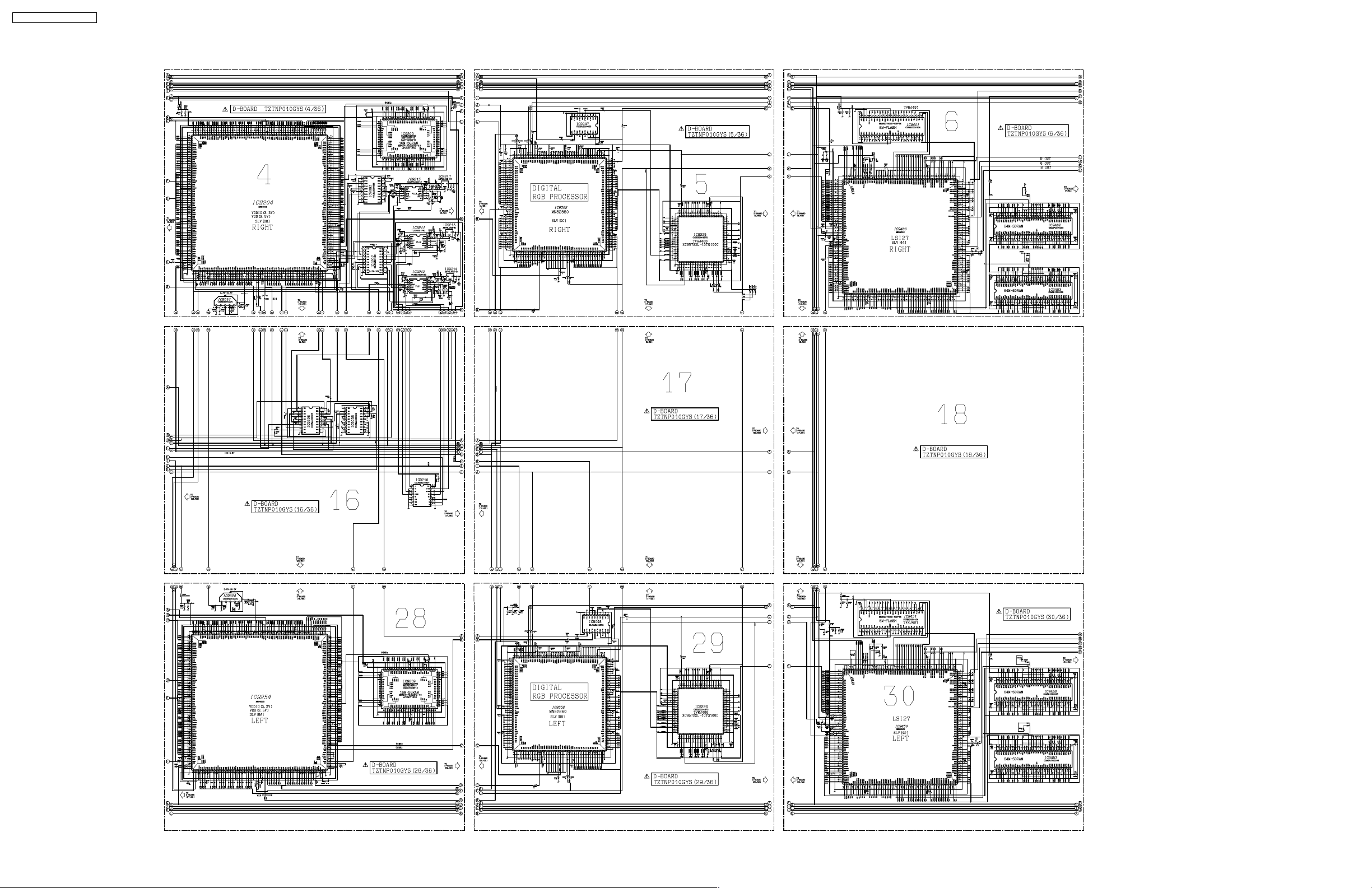
TH-50PHD3 / TH-50PHW3
13.22. D-Board Information (2/4)
92
Page 93
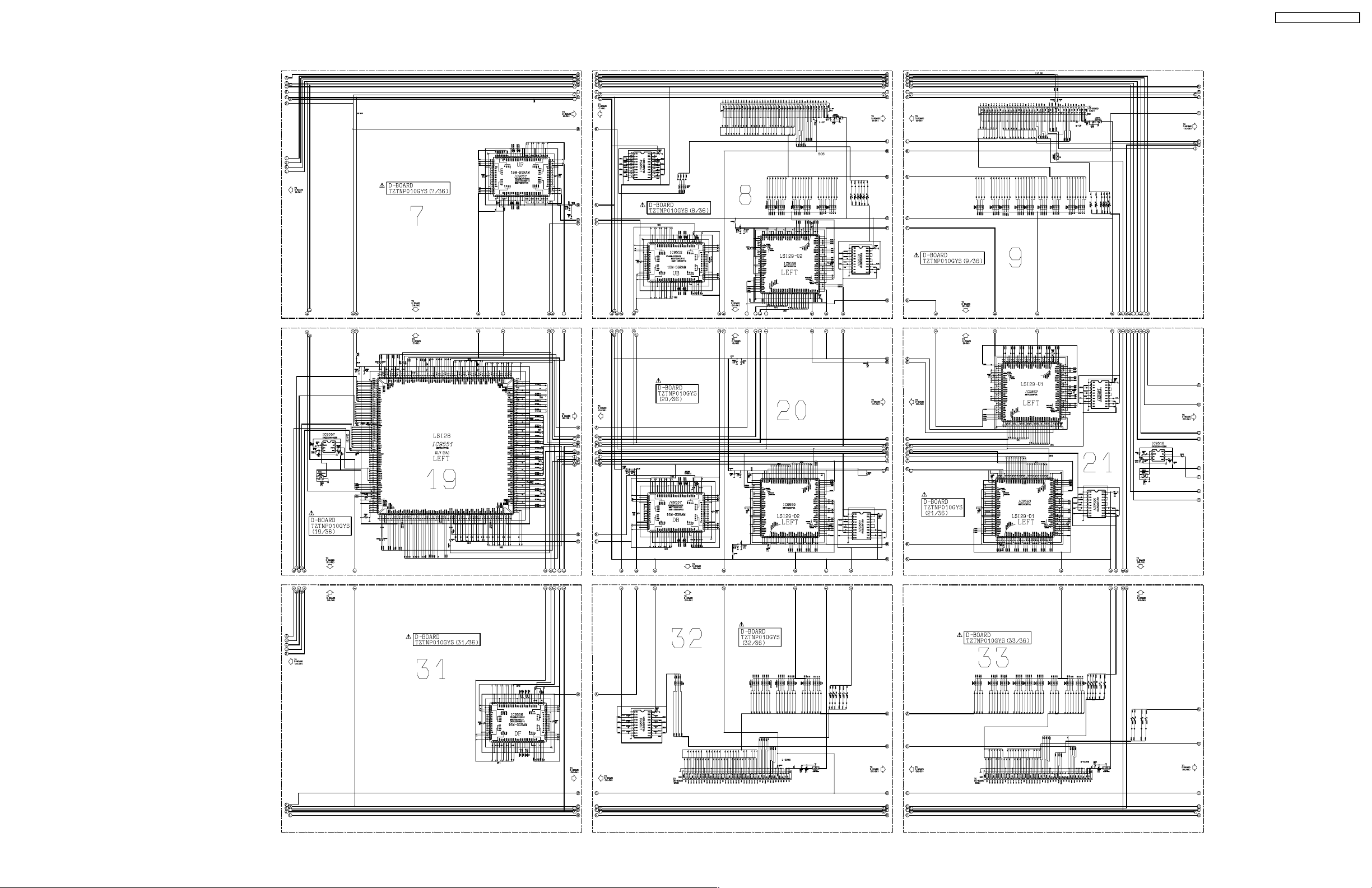
13.23. D-Board Information (3/4)
TH-50PHD3 / TH-50PHW3
93
Page 94
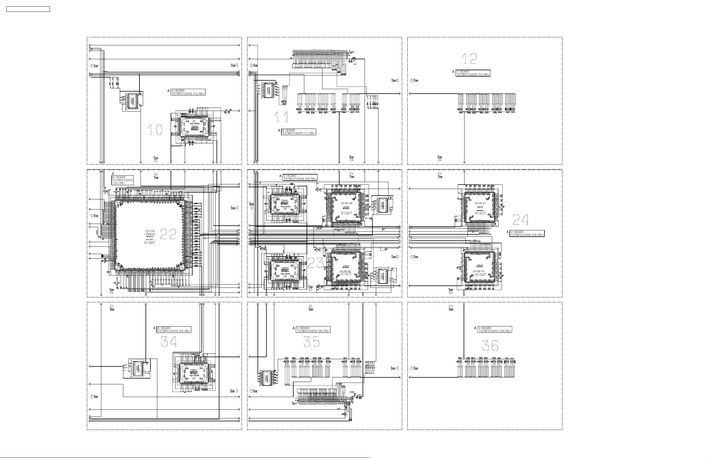
TH-50PHD3 / TH-50PHW3
13.24. D-Board Information (4/4)
94
Page 95
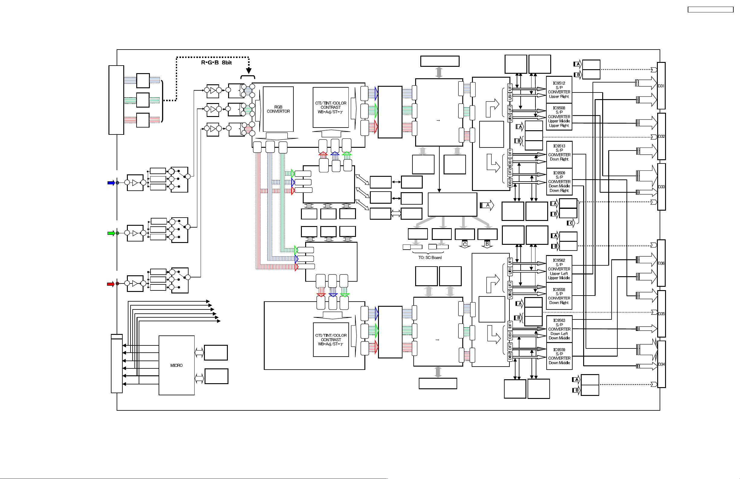
13.25. D-Board Block Diagram
148
14
TH-50PHD3 / TH-50PHW3
D1
3 ~ 6
65~68
8 ~11
60~63
13~16
55~58
15MHz / 525P
20MHz / HD
35MHz / XGA
JK9003
JK9002 IC9000
JK9001
B-IN
G-IN
R-IN
(45)
(26)
(25)
(47)
(48)
(23)
IC9001
3
3
IC9002
3
D1
IC9015
IC9016
IC9017
1
1
1
SCL1
SDA1
SCL2
SDA2
SCL3
SDA3
LC9014 - 16
8MHz
20MHz
35MHz
LC9010 - 12
8MHz
20MHz
35MHz
LC9018 - 20
8MHz
20MHz
35MHz
IC9005
BAND SW.
16
16
9
8
IC9004
BAND SW.
16
9
8
IC9006
BAND SW.
16
9
8
IC9701
IC9401
8M FLASH MEMORY
left
SCL1
SDA1
SCL2
IC9705
17
17
17
SDA2
SCL3
SDA3
IC9007
7
IC9008
7
IC9009
7
A/D
A/D
A/D
19
2
11
26
18
2
11
2
11
11
10
3
34
~ 41
IC9302 IC9352
RGB PROCESSOR
8 BIT
44
~ 51
~ 62
IC9302
IC9403
64M SDRAM
FIELD
MEMORY
IC9900
CONTROL
BUFFER
IC9453
FIELD
171~156191~172
211~192
IC9905
171~156191~172
211~192
R
254
244
55
271-278
281~288
289~296
271-278
281~288
289~296
IC9352
233
~
~
252
242
113
102
~
~95
106
IC9204
FORMAT CONVERTER
(LINE CONVERTER)
I/P CONVERTER
ASPECT CONTROL
4:3 / 16:9
16M
SDRAM
16M
SDRAM
16M
16M
IC9254
4:3 / 16:9
102
~95
244
~
252
SDRAM
SDRAM
94
~87
254
262
SDRAM
SDRAM
FORMAT CONVERTER
IC9201 IC9209
(LINE CONVERTER)
I/P CONVERTER
ASPECT CONTROL
113
~
106
233
~
242
~
262
~87
16M
16M
~
94
L
123~116
135~128
140~147
123~116
135~128
~
7
SUB-FIELD
PROCESSOR
IC9093
BUFFER
IC9207
BUFFER
IC9206
BUFFER
SUB-FIELD
PROCESSOR
IC9225
IC9226
24 ~ 17
16 ~ 918 ~ 1
64M SDRAM
IC9215
PLLM 80MHz
IC9211
PLL2 50MHz
IC9212
PLL1 80MHz
IC9903
BUFFER
2-9 2-9
D21
24 ~ 17
16 ~ 918 ~ 1
IC9400
NEW PLASMA AI
QUASI-12bit PROCESS
8bit
12bit
IC9402
FIELD
MEMORY
IC9904
BUFFER
D20
IC9452
64M SDRAM
FIELD
MEMORY
IC9450
NEW PLASMA AI
QUASI-12bit PROCESS
8bit
12bit
IC9541
8M FLASH MEMORY
DISCHARGE
64M SDRAM
MEMORY
28 ~ 39
14 ~ 252 ~ 13
PROCESSOR
IC9906
BUFFER
SUB-FIELD
PROCESSOR
28 ~ 39
14 ~ 252 ~ 13
IC9501
SUB-FIELD
CLK
IC9551
IC9020
6
IC9019
6
IC9021
6
5
5
5
SC1 SC2 SS
IC9702
1 Mbit VRAM
8 Mbit FLASH
MEMORY
IC9503
16M SDRAM
ODD-LINE
MEMORY
IC9507
16M SDRAM
EVEN-LINE
MEMORY
IC9061
16M SDRAM
ODD-LINE
MEMORY
IC9557
16M SDRAM
EVEN-LINE
MEMORY
IC9502
16MSDRAM
EVEN-LINE
MEMORY
IC9554
BUFFER
IC9520
BUFFER
IC9564
BUFFER
IC9506
16M SDRAM
ODD-LINE
MEMORY
IC9552
16M SDRAM
EVEN-LINE
MEMORY
IC9555
BUFFER
IC9521
BUFFER
IC9565
BUFFER
IC9556
16M SDRAM
ODD-LINE
MEMORY
IC9554
BUFFER
IC9510
BUFFER
IC9555
BUFFER
IC9561
BUFFER
IC9554
BUFFER
IC9560
BUFFER
IC9505
BUFFER
IC9511
BUFFER
24bit
24bit
12bit
24bit
36bit
12bit
24bit
24bit
24bit
12bit
36bit
12bit
Upper
Left
Upper
Middle
Upper
Right
Down
Left
Down
Middle
Down
Right
95
Page 96
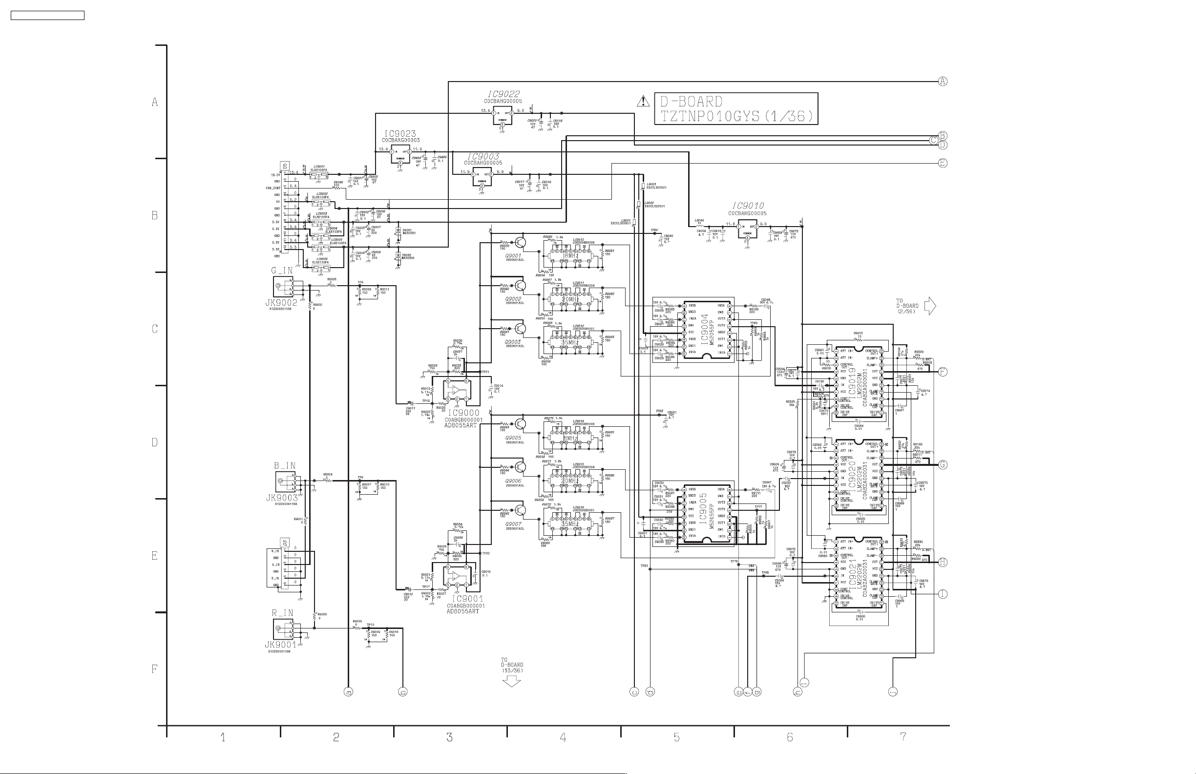
TH-50PHD3 / TH-50PHW3
13.26. D-Board (1/36) Schematic Diagram
96
Page 97
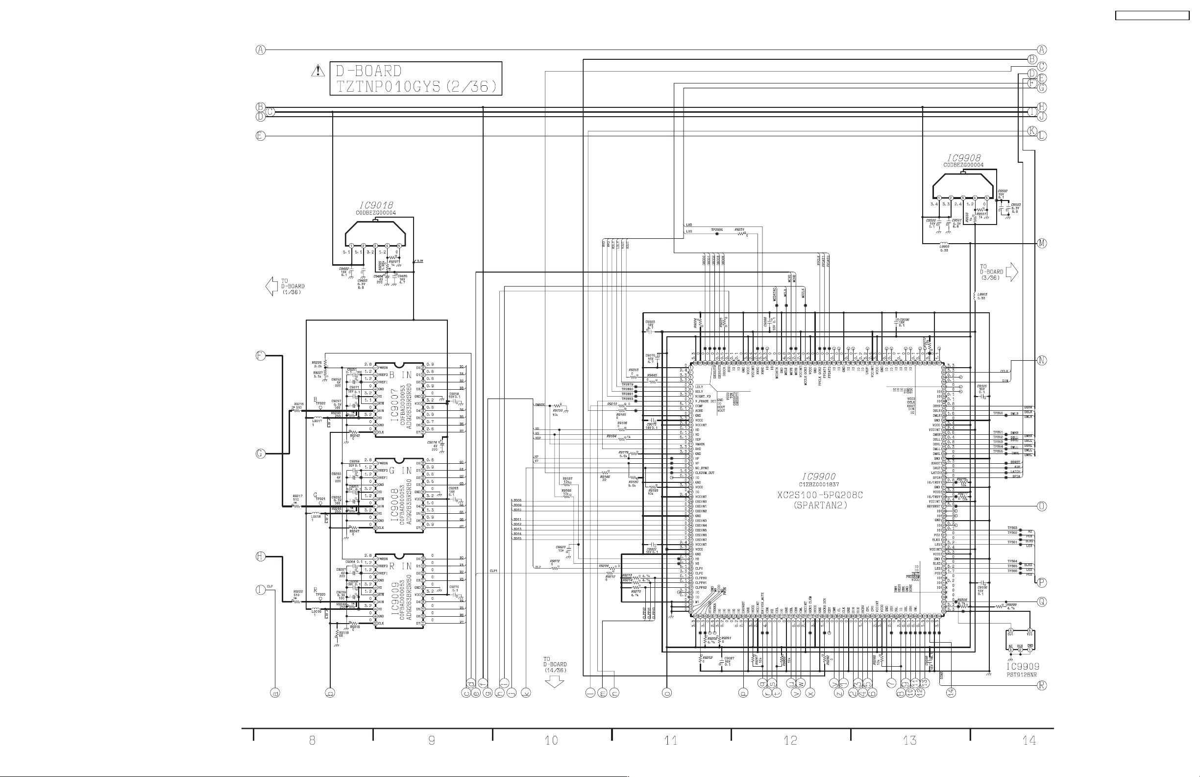
13.27. D-Board (2/36) Schematic Diagram
TH-50PHD3 / TH-50PHW3
97
Page 98
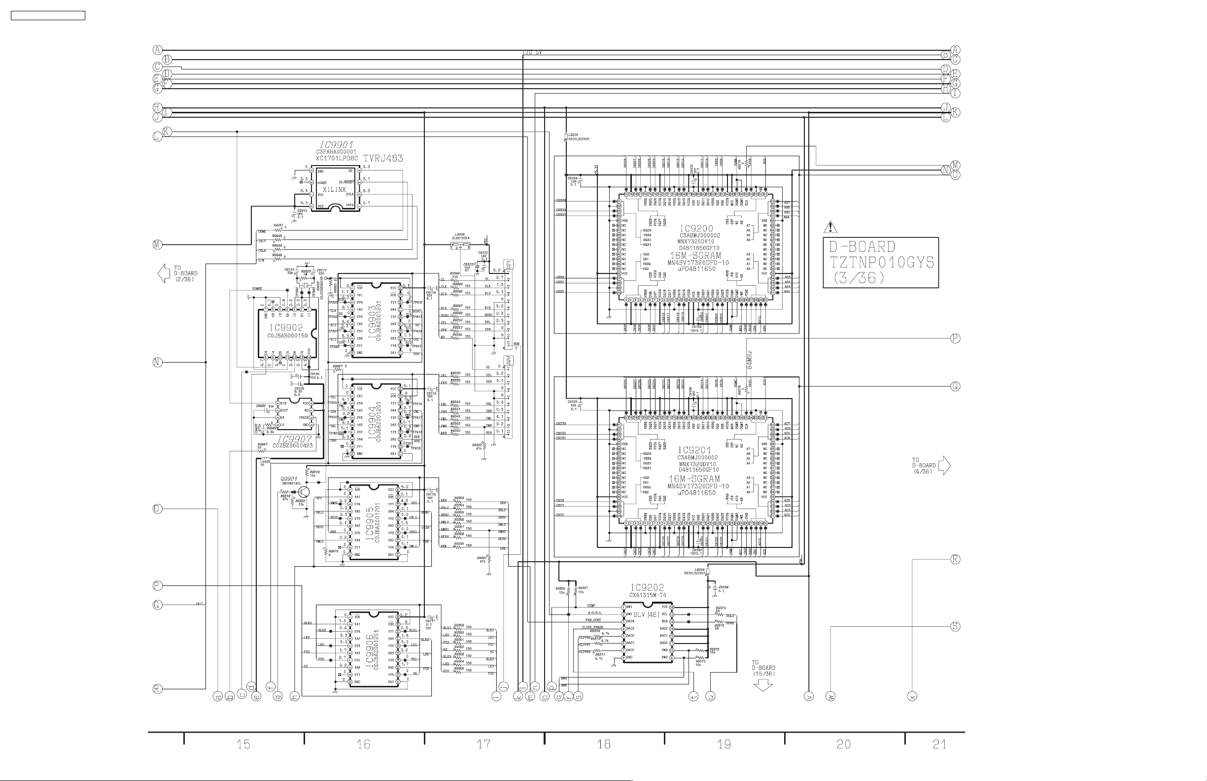
TH-50PHD3 / TH-50PHW3
13.28. D-Board (3/36) Schematic Diagram
98
Page 99
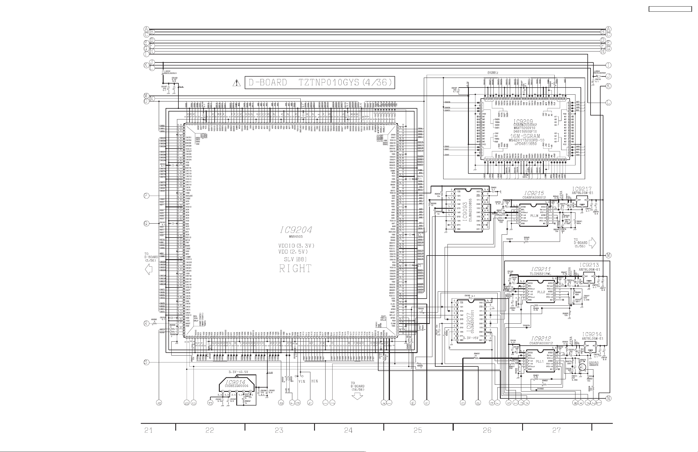
13.29. D-Board (4/36) Schematic Diagram
TH-50PHD3 / TH-50PHW3
99
Page 100
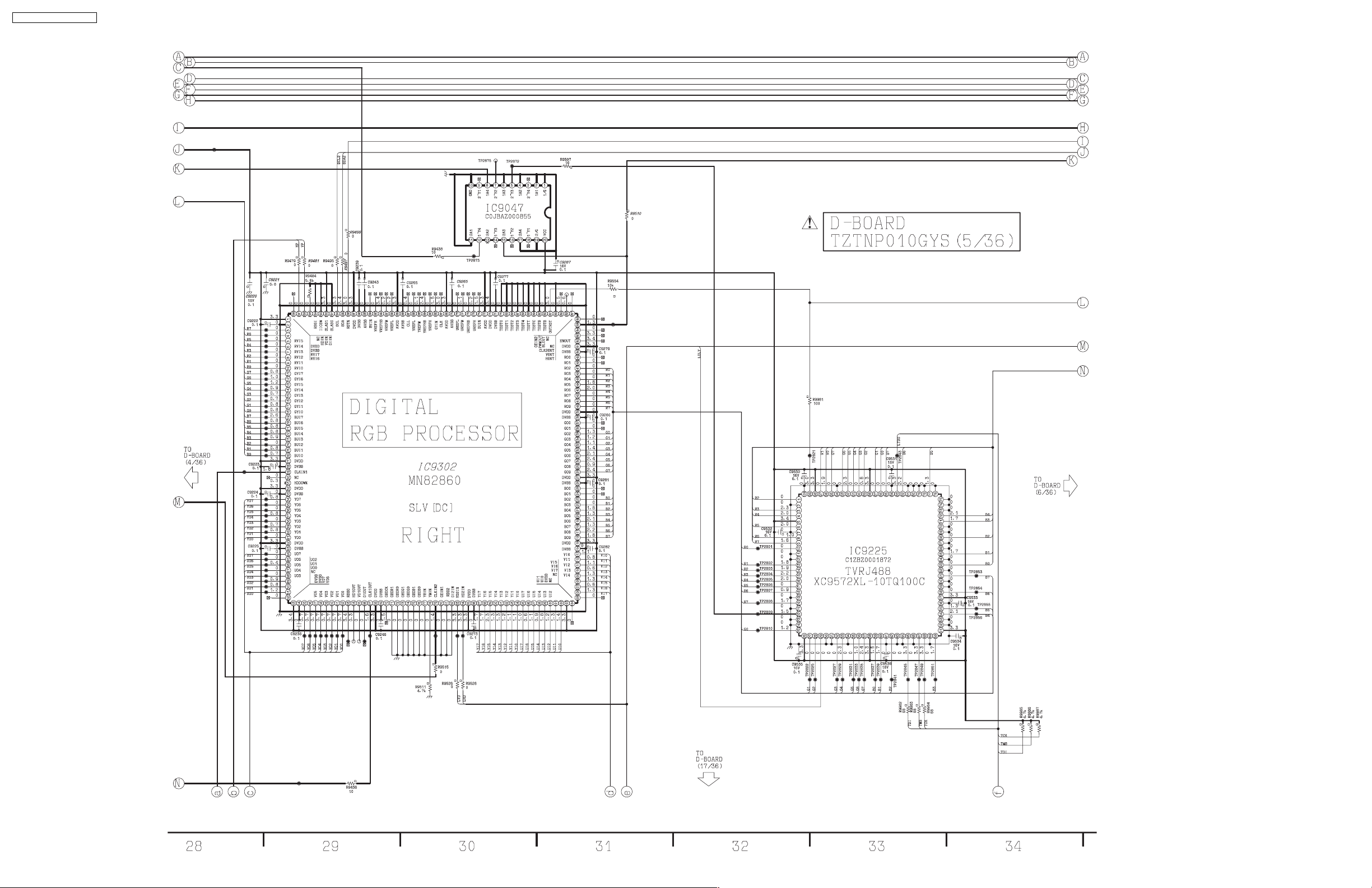
TH-50PHD3 / TH-50PHW3
13.30. D-Board (5/36) Schematic Diagram
100
 Loading...