

Page 1

1
Toshiba Personal Computer
TECRA M4
Maintenance Manual
TOSHIBA CORPORATION
File Number 960-521
[CONFIDENTIAL]
Page 2

Copyright
© 2005 by Toshiba Corporation. All rights reserved. Under the copyright laws, this manual
cannot be reproduced in any form without the prior written permission of Toshiba. No patent
liability is assumed, with respect to the use of the information contained herein.
Toshiba TECRA M4 Maintenance Manual
First edition April 2005
Disclaimer
This manual has been validated and reviewed for accuracy. The instructions and descriptions
it contains are accurate for the Toshiba TECRA M4 at the time of this manual's production.
However, succeeding computers and manuals are subject to change without notice. Toshiba
assumes no liability for damages incurred directly or indirectly from errors, omissions or
discrepancies between the computer and the manual.
Trademarks
IBM is a registered trademark and IBM PC is a trademark of International Business
Machines Corporation.
Intel, Intel SpeedStep and Pentium are trademarks or registered trademarks of Intel
Corporation or its subsidiaries in the United States and other countries/regions.
Windows and Microsoft are registered trademarks of Microsoft Corporation.
Photo CD is a trademark of Eastman Kodak.
Sonic RecordNow! Is registered trademark of Sonic Solutions.
Bluetooth is a trademark owned by its proprietor and used by TOSHIBA under license.
i.LINK is trademark and registered trademark of Sony Corporation.
InterVideo and WinDVD are registered trademarks of the InterVideo Inc.
WinDVD Creator is trademark of the InterVideo Inc.
ii [CONFIDENTIAL] TECRA M4 Maintenance Manual (960-521)
Page 3
Preface
This maintenance manual describes how to perform hardware service maintenance for the
Toshiba Personal Computer TECRA M4, referred to as TECRA M4 in this manual.
The procedures described in this manual are intended to help service technicians isolate
faulty Field Replaceable Units (FRUs) and replace them in the field.
SAFETY PRECAUTIONS
Four types of messages are used in this manual to bring important information to your
attention. Each of these messages will be italicized and identified as shown below.
DANGER: “Danger” indicates the existence of a hazard that could result in death or
serious bodily injury, if the safety instruction is not observed.
WARNING: “Warning” indicates the existence of a hazard that could result in bodily
injury, if the safety instruction is not observed.
CAUTION: “Caution” indicates the existence of a hazard that could result in property
damage, if the safety instruction is not observed.
NOTE: “Note” contains general information that relates to your safe maintenance
service.
Improper repair of the computer may result in safety hazards. Toshiba requires service
technicians and authorized dealers or service providers to ensure the following safety
precautions are adhered to strictly.
Be sure to fasten screws securely with the right screwdriver. Be sure to use the PH
Point size “0” and “1” screwdrivers complying with the ISO/DIS 8764-1:1996. If a
screw is not fully fastened, it could come loose, creating a danger of a short circuit,
which could cause overheating, smoke or fire.
If you replace the battery pack or RTC battery, be sure to use only the same model
battery or an equivalent battery recommended by Toshiba. Installation of the wrong
battery can cause the battery to explode.
TECRA M4 Maintenance Manual (960-521) [CONFIDENTIAL] iii
Page 4

The manual is divided into the following parts:
Chapter 1 Hardware Overview describes the Satellite R10 system unit and each
FRU.
Chapter 2 Troubleshooting Procedures explains how to diagnose and resolve
FRU problems.
Chapter 3 Test and Diagnostics describes how to perform test and diagnostic
operations for maintenance service.
Chapter 4 Replacement Procedures describes the removal and replacement of the
FRUs.
Appendices The appendices describe the following:
Handling the LCD module
Board layout
Pin assignment
Keyboard scan/character codes
Key layout
Wiring Diagrams
BIOS Rewrite Procedures
EC/KBC Rewrite Procedures
Reliability
iv [CONFIDENTIAL] TECRA M4 Maintenance Manual (960-521)
Page 5

Conventions
This manual uses the following formats to describe, identify, and highlight terms and
operating procedures.
Acronyms
On the first appearance and whenever necessary for clarification acronyms are enclosed in
parentheses following their definition. For example:
Read Only Memory (ROM)
Keys
Keys are used in the text to describe many operations. The key top symbol as it appears on
the keyboard is printed in boldface type.
Key operation
Some operations require you to simultaneously use two or more keys. We identify such
operations by the key top symbols separated by a plus (+) sign. For example, Ctrl + Pause
(Break) means you must hold down Ctrl and at the same time press Pause (Break). If
three keys are used, hold down the first two and at the same time press the third.
User input
Text that you are instructed to type in is shown in the boldface type below:
DISKCOPY A: B:
The display
Text generated by the Satellite R10 that appears on its display is presented in the type face
below:
Format complete
System transferred
TECRA M4 Maintenance Manual (960-521) [CONFIDENTIAL] v
Page 6

Table of Contents
Chapter 1 Hardware Overview
1.1 Features......................................................................................................................1-1
1.2 2.5-inch Hard Disk Drive......................................................................................... 1-11
1.3 Optical Drive............................................................................................................ 1-13
1.4 Keyboard..................................................................................................................1-26
1.5 TFT Color Display...................................................................................................1-27
1.6 Power Supply...........................................................................................................1-29
1.7 Batteries ...................................................................................................................1-32
1.8 AC Adapter.............................................................................................................. 1-35
Chapter 2 Troubleshooting Procedures
2.1 Troubleshooting......................................................................................................... 2-1
2.2 Troubleshooting Flowchart........................................................................................2-2
2.3 Power Supply Troubleshooting..................................................................................2-6
2.4 System Board Troubleshooting................................................................................2-17
2.5 USB 3.5” FDD Troubleshooting..............................................................................2-33
2.6 2.5” HDD Troubleshooting...................................................................................... 2-36
2.7 Keyboard Troubleshooting ......................................................................................2-41
2.8 Display Troubleshooting.......................................................................................... 2-42
2.9 Touch Pad Troubleshooting.....................................................................................2-44
2.10 Selectable bay(optical drive) Troubleshooting........................................................2-45
2.11 Modem Troubleshooting.......................................................................................... 2-46
2.12 Bluetooth Troubleshooting ......................................................................................2-47
2.13 LAN Troubleshooting..............................................................................................2-50
2.14 Sound Troubleshooting............................................................................................2-51
2.15 SD Card Slot Troubleshooting................................................................................. 2-52
2.16 Tablet Pen Troubleshooting.....................................................................................2-53
vi [CONFIDENTIAL] TECRA M4 Maintenance Manual (960-521)
Page 7

2.17 Wireless LAN Troubleshooting...............................................................................2-55
Chapter 3 Tests and Diagnostics
3.1 The Diagnostic Test................................................................................................... 3-1
3.2 Executing the Diagnostic Test...................................................................................3-4
3.3 Setting of the hardware configuration........................................................................3-8
3.4 Heatrun Test.............................................................................................................3-11
3.5 Subtest Names.......................................................................................................... 3-12
3.6 System Test.............................................................................................................. 3-14
3.7 Memory Test............................................................................................................ 3-16
3.8 Keyboard Test.......................................................................................................... 3-17
3.9 Display Test.............................................................................................................3-18
3.10 Floppy Disk Test...................................................................................................... 3-21
3.11 Printer Test...............................................................................................................3-23
3.12 Async Test ............................................................................................................... 3-25
3.13 Hard Disk Test.........................................................................................................3-26
3.14 Real Timer Test........................................................................................................3-29
3.15 NDP Test.................................................................................................................. 3-31
3.16 Expansion Test.........................................................................................................3-32
3.17 CD-ROM/DVD-ROM Test ..................................................................................... 3-34
3.18 Error Code and Error Status Names.........................................................................3-35
3.19 Hard Disk Test Detail Status....................................................................................3-38
3.20 Only One Test.......................................................................................................... 3-40
3.21 Head Cleaning.......................................................................................................... 3-48
3.22 Log Utilities.............................................................................................................3-49
3.23 Running Test............................................................................................................ 3-51
3.24 Floppy Disk Drive Utilities......................................................................................3-52
3.25 System Configuration ..............................................................................................3-57
3.26 Wireless LAN Test Program (Intel-made b/g).........................................................3-59
3.27 Wireless LAN Test Program (Intel-made a/b/g)......................................................3-63
3.28 LAN/Modem/Bluetooth/IEEE1394 Test Program .................................................. 3-68
3.29 Sound Test Program.................................................................................................3-82
TECRA M4 Maintenance Manual (960-521) [CONFIDENTIAL] vii
Page 8

3.30 SETUP ....................................................................................................................3-88
Chapter 4 Replacement Procedures
4.1 Overview...................................................................................................................4-1
4.2 Battery pack..............................................................................................................4-8
4.3 PC card/SD card......................................................................................................4-10
4.4 Memory module......................................................................................................4-12
4.5 HDD........................................................................................................................4-14
4.6 Selectable bay module ............................................................................................4-16
4.7 Keyboard.................................................................................................................4-19
4.8 Bottom cover assembly...........................................................................................4-21
4.9 Battery latch assembly/Selectable bay lock............................................................4-23
4.10 QI button assembly/PC card slot brace...................................................................4-25
4.11 Bluetooth module....................................................................................................4-27
4.12 MDC/Modem cable ................................................................................................4-29
4.13 Wireless LAN card .................................................................................................4-32
4.14 Fan/CPU..................................................................................................................4-34
4.15 DC-IN jack..............................................................................................................4-39
4.16 Penholder/RTC battery ...........................................................................................4-40
4.17 LCD harness holder................................................................................................4-42
4.18 Mic (L) cable guide................................................................................................ 4-45
4.19 QI board/CN board ................................................................................................ 4-47
4.20 System board...........................................................................................................4-49
4.21 PC card slot cover ...................................................................................................4-51
4.22 Speaker....................................................................................................................4-52
4.23 Microphone/Front panel..........................................................................................4-53
4.24 Lens holder..............................................................................................................4-57
4.25 Touch pad................................................................................................................4-58
4.26 LCD unit & FL inverter ..........................................................................................4-59
4.27 Application switch board........................................................................................4-63
4.28 LCD latch assembly................................................................................................4-64
4.29 Digitizer ..................................................................................................................4-65
viii [CONFIDENTIAL] TECRA M4 Maintenance Manual (960-521)
Page 9

4.30 LCD harnesses & Wireless LAN/Bluetooth antennas............................................4-71
4.31 Hinge switch Board.................................................................................................4-76
4.32 Fluorescent Lamp....................................................................................................4-77
Appendices
Appendix A Handling the LCD Module .......................................................................A-1
Appendix B Board Layout ............................................................................................B-1
Appendix C Pin Assignment ......................................................................................... C-1
Appendix D Keyboard Scan/Character Codes ..............................................................D-1
Appendix E Key Layout.................................................................................................E-1
Appendix F Wiring Diagrams........................................................................................F-1
Appendix G BIOS Rewrite Procedures.........................................................................G-1
Appendix H EC/KBC Rewrite Procedures.................................................................... H-1
Appendix I Reliability....................................................................................................I-1
TECRA M4 Maintenance Manual (960-521) [CONFIDENTIAL] ix
Page 10

x [CONFIDENTIAL] TECRA M4 Maintenance Manual (960-521)
Page 11

Chapter 1
Hardware Overview
[CONFIDENTIAL]
Page 12

1 Hardware Overview
1 Hardware Overview
1-ii [CONFIDENTIAL] TECRA M4 Maintenance Manual (960-521)
Page 13

1 Hardware Overview
Chapter 1 Contents
1.1 Features...................................................................................................................... 1-1
1.2 2.5-inch Hard Disk Drive......................................................................................... 1-11
1.3 Optical Drive............................................................................................................ 1-13
1.3.1 DVD-ROM Drive............................................................................... 1-13
1.3.2 DVD-ROM & CD-R/RW Drive ........................................................ 1-16
1.3.3 DVD Super Multi Drive..................................................................... 1-19
1.3.4 DVD Super Multi Drive (Double-layer)............................................ 1-22
1.4 Keyboard.................................................................................................................. 1-26
1.5 TFT Color Display................................................................................................... 1-27
1.5.1 LCD Module ...................................................................................... 1-27
1.5.2 FL Inverter Board............................................................................... 1-28
1.6 Power Supply........................................................................................................... 1-29
1.7 Batteries ...................................................................................................................1-32
1.7.1 Main Battery....................................................................................... 1-32
1.7.2 Battery Charging Control...................................................................1-33
1.7.3 RTC Battery .......................................................................................1-34
1.8 AC Adapter.............................................................................................................. 1-35
TECRA M4 Maintenance Manual (960-521) [CONFIDENTIAL] 1-iii
Page 14

1 Hardware Overview
Figures
Figure 1-1 Front of the computer.....................................................................................1-5
Figure 1-2 System units configuration ............................................................................ 1-6
Figure 1-3 System Block Diagram ..................................................................................1-7
Figure 1-4 2.5-inch HDD............................................................................................... 1-11
Figure 1-5 DVD-ROM drive ......................................................................................... 1-13
Figure 1-6 DVD-ROM & CD-R/RW drive................................................................... 1-16
Figure 1-7 DVD Super Multi drive ............................................................................... 1-19
Figure 1-8 DVD Super Multi drive (Double-layer)....................................................... 1-22
Figure 1-9 Keyboard...................................................................................................... 1-26
Figure 1-10 LCD module.................................................................................................1-27
Tables
Table 1-1 2.5-inch HDD Specifications....................................................................... 1-11
Table 1-2 DVD-ROM drive outline dimensions..........................................................1-13
Table 1-3 DVD-ROM drive specifications.................................................................. 1-14
Table 1-4 DVD-ROM & CD-R/RW drive outline dimensions.................................... 1-16
Table 1-5 DVD-ROM & CD-R/RW drive specifications............................................ 1-17
Table 1-6 DVD Super Multi drive outline dimensions................................................ 1-19
Table 1-7 DVD Super Multi drive specifications ........................................................ 1-20
Table 1-8 DVD Super Multi drive (Double-layer) outline dimensions .......................1-22
Table 1-9 DVD Super Multi drive (Double-layer) specifications................................ 1-23
Table 1-10 LCD module specifications (14.1 TFT).......................................................1-27
Table 1-11 FL inverter board specifications ..................................................................1-28
Table 1-12 Power supply output specifications ............................................................. 1-30
Table 1-13 Battery specifications................................................................................... 1-32
Table 1-14 Time required for charges of main battery .................................................. 1-33
Table 1-15 Data preservation time................................................................................. 1-33
Table 1-16 RTC battery charging/data preservation time..............................................1-34
1-iv [CONFIDENTIAL] TECRA M4 Maintenance Manual (960-521)
Page 15

1 Hardware Overview
Table 1-17 AC adapter specifications............................................................................1-35
TECRA M4 Maintenance Manual (960-521) [CONFIDENTIAL] 1-v
Page 16

1.1 Features 1 Hardware Overview
1 Features
1.1 Features
The TECRA M4 is an ultra thin and lightweight tablet PC realizing cable-less environment
on a table by wireless function with a Intel ® Mobile Pentium ®-M processor realizing high
performance.
Microprocessor
Microprocessor that is used will be different of the model.
¾ Intel ® Mobile Pentium ®-M Processor
1.60GHz (Processor Number ; 730)
1.73GHz (Processor Number ; 740)
1.86GHz (Processor Number ; 750)
2.00GHz (Processor Number ; 760)
2.13GHz (Processor Number ; 770)
PPV: 0.748 to 1.308
L1 cache : 64KB (32KB(Code) + 32KB(Data))
L2 cache : 2MB
Chipset
Equipped with Intel 915PM as North Bridge, Intel ICH6-M as South Bridge and
Texas Instrument PCI7411ZHK as Card Controller.
GPU Controller
Equipped with a nVIDIA MEP43L with 64MB/128MB.
Memory
Two DDR2 SO-DIMM slots support DDR2 400 or DDR2 533. Memory modules can
be installed to a maximum of 2GB (2,048MB). Memory modules of 256MB, 512MB
and 1GB sizes are available.
HDD
Single SATA 40/60/80/100GB internal drive. 2.5-inch x 9.5mm height
TECRA M4 Maintenance Manual (960-521) [CONFIDENTIAL] 1-1
Page 17

1 Hardware Overview 1.1 Features
Selectable Bay
Supporting hot-swap with DVD-ROM drive, DVD-ROM & CD-R/RW drive, DVD
nd
Super Multi drive, 2
HDD adapter and 2nd battery.
USB FDD
3.5 inch USB FDD supports 720KB/1.44MB formats.
Display
Display swivels automatically 0/90/180/270 degrees by display driver. LCD and CRT
can be displayed at the same time.
LCD Built-in 14.1 inch, 16M colors, SXGA+ (1,400×1,050 dots), thin type low
temperature poly-silicon TFT color display.
External monitor Supported via an RGB connector
Video-out Supported via an S-Video connector
Digitizer
Digitizer is installed at the rear of LCD unit. The supplied tablet pen enables pen
computing.
Tablet pen / Reserve pen
Tablet pen / Reserve pen can be used as a mouse by touching the display softly with
the pen tip. Tablet button on the side of the pen corresponds to the right click of the
mouse. Erase button on the pen tail can be used as an eraser depending on the
application.
Keyboard
Keyboard has 85(US)/86(UK)-key with a pointing stick (AccuPoint) and supports
Windows key and Hot key.
Touch pad
Touch pad is installed as a pointing device.
Batteries
The computer has two batteries: a rechargeable Lithium-Ion main battery pack and an
RTC battery (that backs up the Real Time Clock and CMOS memory).
1-2 [CONFIDENTIAL] TECRA M4 Maintenance Manual (960-521)
Page 18

1.1 Features 1 Hardware Overview
USB (Universal Serial Bus)
Three USB ports are usable. The ports comply with the USB2.0 standard, which
enables data transfer speeds 40 times faster than USB1.1 standard. USB1.1 is also
supported.
PC card slot
The PC card slot (PCMCIA) accommodates one 5mm Type II card. (Based on PC
Card Standard, supporting CardBus)
SD card slot
A SD Card Slot can accommodate Secure Digital flash memory cards with various
capacities. Supporting memory card and I/O card.
Sound system
The sound system is equipped with the following features:
- Built-in stereo speakers
- Built-in monaural microphone
- Stereo Headphone jack (3.5mm mini headphone jack)
- External microphone jack (3.5mm mini microphone jack)
Switch/Button
Windows Security tablet button, ESC/Rotation button, Cross Function button,
Toshiba Application button and Wireless communication switch are available.
Internal Modem
The internal modem is equipped as a modem daughter card (MDC).
The internal modem provides capability for data and fax communication and supports
ITU-T V.90 standard. For data reception it operates at 56Kbps and for data
transmission it operates at 33.6Kbps. For fax transmission, it operates at 14,4Kbps.
The speed of data transfer and fax depends on analog telephone line condition. It has
an RJ11 modem jack for connecting to a telephone line.
LAN
The internal LAN supports 10/100Mbit or Gigabit Ethernet.
TECRA M4 Maintenance Manual (960-521) [CONFIDENTIAL] 1-3
Page 19

1 Hardware Overview 1.1 Features
Wireless LAN
Wireless LAN Card can be equipped with mini-PCI slot. Based on IEEE802.11b/g,
a/b/g with 2.45GHz/5.0GHz Dual-band antenna.
i.LINK (IEEE1394)
This port enables high-speed data transfer directly from external devices such as
digital video cameras.
Docking port
Advanced Port Replicator III and Tablet Multi Dock II can be connected through
docking port on the bottom.
Infrared port
The infrared port is compatible with Fast infrared (FIR) standards enabling wireless
4 Mbps, 1.152 Mbps, 115.2 kbps, 57.6 kbps, 38.4 kbps, 19.2 kbps or 9.6 kbps data
transfer with Infrared Data Association (IrDA) 1.1 compatible external devices.
Bluetooth
The computer is equipped with Bluetooth (V1.2) communications standard that
enables wireless connection between electronic devices such as computers and
printers. It supports wireless communication switch.
1-4 [CONFIDENTIAL] TECRA M4 Maintenance Manual (960-521)
Page 20

1.1 Features 1 Hardware Overview
Figure 1-1 shows the front of the computer and Figure 1-2 shows the system units
configuration.
Figure 1-1 Front of the computer
TECRA M4 Maintenance Manual (960-521) [CONFIDENTIAL] 1-5
Page 21

1 Hardware Overview 1.1 Features
Figure 1-2 System units configuration
1-6 [CONFIDENTIAL] TECRA M4 Maintenance Manual (960-521)
Page 22

1.1 Features 1 Hardware Overview
Figure 1-3 shows the system block diagram.
Figure 1-3 System Block Diagram
TECRA M4 Maintenance Manual (960-521) [CONFIDENTIAL] 1-7
Page 23

1 Hardware Overview 1.1 Features
The PC contains the following components.
CPU
¾ Intel ® Mobile Pentium ®-M Processor
1.60GHz (Processor Number ; 730)
1.73GHz (Processor Number ; 740)
1.86GHz (Processor Number ; 750)
2.00GHz (Processor Number ; 760)
2.13GHz (Processor Number ; 770)
Core voltage : 0.748 to 1.308
FSB : 533MHz
L1 cache : 64KB [32KB (Code) + 32KB (Data)]
L2 cache : 2MB
Support : Geyservile III , Deeper Sleep Mode
Memory
Two DDR2 SO-DIMM slots support DDR2 400/DDR2 533 Memory modules in
256MB, 512 MB and 1GB can be installed to a maximum of 2GB (2,048MB).
1.8V operation
240 pin, SO Dual In-line Memory Modules (SO-DIMM)
Supports PC3200/PC4300
BIOS ROM (Flash memory)
8Mbit
1-8 [CONFIDENTIAL] TECRA M4 Maintenance Manual (960-521)
Page 24

1.1 Features 1 Hardware Overview
PCI chipset
This gate array incorporates the following elements and functions
Intel 915PM (North Bridge)
- Dothan Processor System Bus Support
- System Memory Interface
- Memory Control: supports DDR333, DDR2-400/DDR2-533 2Gbmax.
- Graphics I/F: x16 PCI Express Based Graphics I/F
- DMI(Direct Media Interface)
- 1,257-ball, 40.0×37.5×2.6mm, FC-BGA package
Intel ICH6-M (South Bridge)
- DMI(Direct Media Interface)
- PCI Express I/F (4 ports)
- PCI Bus I/F Rev2.3(7 PCI REQ/GNT Pairs)
- Integrated Serial ATA Host Controller (2 Prots,150MB/S)
- Integrated IDE Controller(Ultra ATA 100/66/33)
- AC’97 2.3 codecs
- USB 1.1/2.0 Controller 8 ports (EHCI: Enhanced Host Controller)
- Built-in LAN controller (WfM 2.0 & IEEE 802.3 compliance)
- Power Management (ACPI 2.0 compliance)
- SMBus2.0 controller
- FWH interface (BIOS)
- LPC interface (EC/KBC, Super I/O)
- IRQ controller
- Serial Interrupt Function
- Suspend/Resume control
- Built –in RTC
- GPIO
- 609-ball, 31×31mm, micro BGA Package
PC Card Controller (Texas Instruments-made PCI7411ZHK)
- PCI interface
- CardBus/Ultra Media controller
- SD card controller
- IEEEE1394 controller
- 288-ball (16x16x1.4) BGA package
TECRA M4 Maintenance Manual (960-521) [CONFIDENTIAL] 1-9
Page 25

1 Hardware Overview 1.1 Features
GPU controller (Internal graphic controller)
- VRAM 64/128MB
- PCI Express interface
- LCD I/F LVDS 2ch
- S-video support
Batteries
The main battery is a detachable lithium-ion main battery (10.8V, 4700mAh, 6 cell)
and the RTC battery is a lithium ion battery (2.4V-16mAh).
Modem controller
Supported by MDC. Using of the secondary AC97 Line
LAN controller (Marvell made)
Controls LAN and supports 10/100Mbit or Gigabit Ethernet.
Other main system chips
- EC/KBC (Mitsubishi-made LPC microcontroller M306KAFCLRP)
- PSC (Toshiba-made TMP87PM48UG)
- Temperature sensor (ADM-made ADM1032ARMZ)
- Acceleration sensor (ST Micro-made LIS3L02AQ)
- Super I/O (SMSC-made LPC47N217-JN)
- SOUND CODEC (ADM-made AD1981B)
- AMP (Matsushita-made MM1667XHFE) + HP AMP (MAX4410)
- CLK Generator (ICS-made ICS950812CGLFT)
1-10 [CONFIDENTIAL] TECRA M4 Maintenance Manual (960-521)
Page 26

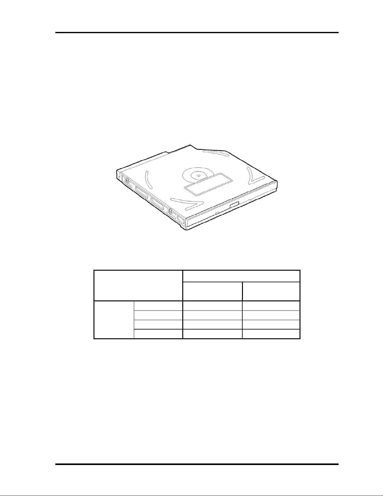
1.2 2.5-inch Hard Disk Drive 1 Hardware Overview
1.2 2.5-inch Hard Disk Drive
A compact, high-capacity SATA HDD with a height of 9.5mm contains a 2.5-inch magnetic
disk and magnetic heads.
Figure 1-4 shows a view of the 2.5-inch HDD and Tables 1-1 list the specifications.
Figure 1-4 2.5-inch HDD
Table 1-1 2.5-inch HDD Specification (1/2)
Specifications
Items
Outline Width (mm)
dimensions Height (mm)
Depth (mm)
Weight (g)
Storage size (formatted) 40GB 60GB 80GB
Speed (RPM) 5,400
Data transfer rate
Media
Host
Data buffer size (MB) 8
Average random seek time
(ms) Read
FUJITU
G8BC0001R410
1.5Gb/s (Serial-ATA Generation-1)
FUJITU
G8BC0001R610
70
9.5
100
99 max.
53.9MB/s max
12
FUJITU
G8BC0001R810
TECRA M4 Maintenance Manual (960-521) [CONFIDENTIAL] 1-11
Page 27
1 Hardware Overview 1.2 2.5-inch Hard Disk Drive
Table 1-1 2.5-inch HDD Specifications(2/2)
Specifications
Items
Outline Width (mm)
dimensions Height (mm)
Depth (mm)
Weight (g)
Storage size (formatted) 100GB
Speed (RPM) 5400
TOSHIBA
HDD2D30BZK01
100
9.5
69.85
98
Data transfer speed (MB/s)
Internal
Host
Data buffer size (MB) 8
Access time (ms)
Average seek time
Track to Track
Max seek
236.1-456.0
150
12
2
22
1-12 [CONFIDENTIAL] TECRA M4 Maintenance Manual (960-521)
Page 28
1.3 Optical Drive 1 Hardware Overview
1.3 Optical Drive
1.3.1 DVD-ROM Drive
The DVD-ROM drive accommodates either 12 cm (4.72-inch) or 8 cm (3.15-inch) CD/DVDROM and CD-R/RW and DVD-RAM (read-only).
The DVD-ROM drive is shown in Figure 1-5. The dimensions and specifications of the
DVD-ROM & CD-R/RW drive are described in Table 1-2, Table 1-3.
Figure 1-5 DVD-ROM drive
Table 1-2 DVD-ROM drive outline dimensions
Specifications
Items
Outline Width (mm)
dimensions Height (mm)
Depth (mm)
Weight (g)
TSST
G8BC0002B410
128±0.2
12.7±0.2
126.1 129.4
170 180
TEAC
G8BC0002E410
128.0
12.7
TECRA M4 Maintenance Manual (960-521) [CONFIDENTIAL] 1-13
Page 29
1 Hardware Overview 1.3 Optical Drive
Table 1-3 DVD-ROM drive specifications (1/2)
Parameter
Data transfer
speed
Access time
(ms)
Buffer memory 256KByte
Supported disk
format
Drive Specification
TSST (G8CC0002B410)
DVD-ROM(Single-L) MAX 8x(CAV) [MAX 10816KB/s]
DVD-ROM(Double-L) MAX 6x(CAV) [MAX 8112KB/s]
DVD-R/-RW MAX 4x(CAV) [MAX 5408KB/s]
DVD+R/+RW MAX 4x(CAV) [MAX 5408KB/s]
Read
ATAPI interface
(MB/s)
CD-ROM 110 (Random)
DVD-ROM 110 (Random)
DVD-RAM 140 (Random)
CD
DVD
DVD-RAM(Ver2.1) MAX 2x(ZCLV) [MAX 2704KB/s]
CD(Mode1) MAX 24x(CAV) [MAX 3600KB/s]
CD(Mode2) MAX 24x(CAV) [MAX 4104KB/s]
CD-DA(Mode1) MAX 10x(CLV) [MAX 1500KB/s]
CD-DA(Mode2) MAX 10x(CLV) [MAX 1710KB/s]
PIO mode16.7 MB/s PIO-MODE4 supported
DMA mode16.7 MB/s MultiwordDMA-MODE2 supported
Ultra DMA mode 33.3 MB/s UltraDMA-MODE2 supported
CD-DA, CD+(E)G, CD-MIDI, CD-TEXT, CD-ROM,
CD-ROM XA, CD-I, CD-I Bridge(Photo-CD, Video-CD),
Multi-session CD(Photo-CD, CD-EXTRA, CD-R,
CD-RW, Portfolio),CD-R, CD-RW
DVD-ROM (DVD-5, DVD-9, DVD-10, DVD-18),
DVD-R (Ver1.0, Ver2.1), DVD-RW (Ver1.0, Ver1.1),
DVD+R, DVD+RW, DVD-RAM (Version2.1)
1-14 [CONFIDENTIAL] TECRA M4 Maintenance Manual (960-521)
Page 30
1.3 Optical Drive 1 Hardware Overview
Table 1-3 DVD-ROM drive specifications (2/2)
Parameter
Data transfer
speed
Access time
(ms)
Buffer memory 256K
Supported disk
format
Drive Specification
TEAC (G8CC0002E410)
DVD-ROM MAX 8x(CAV) [MAX 4594KB/s]
DVD-VIDEO MAX 4x(CAV) [MAX 2297KB/s]
DVD-R/RW MAX 8x(CAV) [MAX 4594KB/s]
Read
ATAPI interface
(MB/s)
CD-ROM 120 (Random)
DVD-ROM 130 (Random)
CD
DVD
DVD-RAM(4.7GB) MAX 5x(CAV) [MAX 3246KB/s]
DVD-RAM(2.6GB) MAX 2.5x(CAV) [MAX 1626KB/s]
CD(Mode1) MAX 24x(CAV) [MAX 5137KB/s]
CD(Mode2) MAX 20x(CAV) [MAX 4280KB/s]
CD-RW MAX 24x(CLV) [MAX 5137KB/s]
PIO mode16.7 MB/s PIO-MODE4 supported
DMA mode16.7 MB/s MultiwordDMA-MODE2 supported
Ultra DMA mode 33.3 MB/s UltraDMA-MODE2 supported
CD-DA, CD-ROM MODE1, CD-ROM MODE2,
Multi-session CD, Video-CD, Enhanced CD,
CD-TEXT, Photo-CD, addressing Method 2
DVD-ROM
DVD-R (General, Authoring, Single/Multi-boarder),
DVD-Video, DVD-RW (Single/Multi-boarder, Packet),
DVD-RAM (4.7GB, 2.6GB),
DVD+R/RW (Single/Multi-boarder, Packet)
TECRA M4 Maintenance Manual (960-521) [CONFIDENTIAL] 1-15
Page 31

1 Hardware Overview 1.3 Optical Drive
1.3.2 DVD-ROM & CD-R/RW Drive
The DVD-ROM & CD-R/RW drive accommodates either 12 cm (4.72-inch) or 8 cm (3.15inch) CD/DVD-ROM and CD-R/RW.
The DVD-ROM & CD-R/RW drive is shown in Figure 1-6. The dimensions and
specifications of the DVD-ROM & CD-R/RW drive are described in Table 1-4, Table 1-5.
Figure 1-6 DVD-ROM & CD-R/RW drive
Table 1-4 DVD-ROM & CD-R/RW drive outline dimensions
Parameter Standard value
Outline
dimensions
Maker (code)
Width (mm) 128
Height (mm) 12.7 (excluding projections)
Depth (mm) 129.0
Mass (g) 190±10
PCC
(G8CC0001X411)
TEAC
(G8CC0001Y411)
1-16 [CONFIDENTIAL] TECRA M4 Maintenance Manual (960-521)
Page 32

1.3 Optical Drive 1 Hardware Overview
Table 1-5 DVD-ROM & CD-R/RW drive specifications (1/2)
Parameter
Data transfer
speed
Access time
(ms)
Buffer memory 2MB
Supported disk
format
Drive Specification
PCC (G8CC0001X411)
Read
Write
ATAPI interface
(MB/s)
CD-ROM 150 (Random)
DVD-ROM 180 (Random)
CD
DVD
DVD-ROM MAX 8x(CAV) [MAX 10800 KB/s]
CD-ROM MAX 24x(CAV) [MAX 3600 KB/s]
CD-R 4x/8x(CLV), 16x(PCAV), MAX24x(CAV)
CD-RW 4x(CLV)
High Speed CD-RW 4x/8x/10x(CLV)
Ultra Speed CD-RW 10x(CLV), MAX24x(CAV)
PIO mode16.6 MB/s PIO MODE4 supported
DMA mode16.6 MB/s Multiword MODE2 supported
Ultra DMA mode 33.3 MB/s Ultra DMA MODE2
CD-DA,CD-ROM,CD-ROM XA
Photo CD, CD-Extra(CD+), CD-text
DVD-R (DVD-R Multi-boarder supported)
DVD-RW(Ver.1.1), DVD-Video, DVD+R, DVD+RW,
DVD-RAM(2.6GB/4.7GB)
TECRA M4 Maintenance Manual (960-521) [CONFIDENTIAL] 1-17
Page 33

1 Hardware Overview 1.3 Optical Drive
Table 1-5 DVD-ROM & CD-R/RW drive specifications (2/2)
Parameter
Data transfer
speed
Access time
(ms)
Buffer memory 2MB
Supported disk
format
Drive Specification
TEAC (G8CC0001Y411)
Read
Write
ATAPI interface
(MB/s)
CD-ROM 90 (Random)
DVD-ROM 110 (Random)
CD
DVD
DVD-ROM MAX 8x(CAV) [MAX 10800 KB/s]
CD-ROM MAX 24x(CA V ) [MAX 3600 KB/s]
CD-R 4x/10x(CLV), 16x(CAV), MAX 24x(CAV)
CD-RW 4x(CLV)
High Speed CD-RW 4x/10x(CLV), 10x(CAV)
Ultra Speed CD-RW 10x(CLV), MAX 24x(CAV)
PIO mode16.6 MB/s PIO MODE4 supported
DMA mode16.6 MB/s Multiword MODE2 supported
Ultra DMA mode 33.3 MB/s Ultra DMA MODE2
CD-DA,CD-ROM,CD-ROM XA
Photo CD, CD-Extra(CD+), CD-text
DVD-R (DVD-R Multi-boarder supported)
DVD-RW(Ver.1.2), DVD-Video, DVD+R, DVD+RW,
DVD-RAM(2.6GB/4.7GB)
1-18 [CONFIDENTIAL] TECRA M4 Maintenance Manual (960-521)
Page 34

1.3 Optical Drive 1 Hardware Overview
1.3.3 DVD Super Multi Drive
The DVD Super Multi drive accommodates either 12 cm (4.72-inch) or 8 cm (3.15-inch)
CD/DVD-ROM, CD-R/RW, DVD±R/±RW and DVD-RAM.
The DVD Super Multi drive is shown in Figure 1-7. The dimensions and specifications of the
DVD Super Multi drive are described in Table 1-6, Table 1-7.
Outline
dimensions
Figure 1-7 DVD Super Multi drive
Table 1-6 DVD Super Multi drive outline dimensions
Parameter Standard value
Maker PCC
(G8CC00021410)
Width (mm) 128 128
Height (mm) 12.7 (excluding
projections)
Depth (mm) 129.0 129.0
Mass (g) 210±10 190±10
PCC
(G8CC0002F412)
12.7 (excluding
projections)
TECRA M4 Maintenance Manual (960-521) [CONFIDENTIAL] 1-19
Page 35

1 Hardware Overview 1.3 Optical Drive
Table 1-7 DVD Super Multi drive specifications (1/2)
Parameter
Data transfer
speed
Access time
(ms)
Buffer memory 2MB
Supported disk
format
Drive Specification
PCC (G8CC00021410)
Read(KB/s)
Write
ATAPI interface
(MB/s)
CD-ROM 150 (Random)
DVD-ROM 180 (Random)
CD
DVD
DVD-ROM MAX 8x(CAV) [MAX 10800 KB/s]
CD-ROM MAX 24x(CAV) [MAX 3600 KB/s]
CD-R 4x/8x (CLV), 24x (ZCLV)
CD-RW 4x (CLV)
High Speed CD-RW 4x/8x/10x (CLV)
Ultra Speed CD-RW 10x (CLV)
DVD-R 1x/2x (CLV), MAX 8x (CLV)
DVD-RW 1x/2x (CLV), MAX 4x (CLV)
DVD+R 2.4x (CLV), MAX 8x (CLV)
DVD+RW 2.4x (CLV), MAX 4x (CLV)
DVD-RAM 3x (ZCLV) (4.7GB/9.4GB)
PIO mode 16.6 MB/s (PIO MODE4 supported)
DMA mode 16.6 MB/s (Multi-ward MODE2 supported)
Ultra DMA mode 33.3 MB/s(Ultra DMA MODE2 supported)
CD-DA, CD-ROM, CD-ROM XA,
Photo CD, CD-Extra(CD+), CD-text
DVD-R, DVD-RW (Ver1.1),
DVD Video, DVD+R, DVD+RW,
DVD-RAM (2.6GB/4.7GB)
1-20 [CONFIDENTIAL] TECRA M4 Maintenance Manual (960-521)
Page 36

1.3 Optical Drive 1 Hardware Overview
Table 1-7 DVD Super Multi drive specifications (2/2)
Parameter
Data transfer
speed
Access time
(ms)
Buffer memory 2MB
Supported disk
format
Drive Specification
PCC(G8CC0002F412)
Read(KB/s)
Write
ATAPI interface
(MB/s)
CD-ROM 150 (Random) (typ.)
DVD-ROM 180 (Random) (typ.)
CD
DVD
DVD-ROM MAX 8x(CAV) [MAX 10800 KB/s]
CD-ROM MAX 24x(CAV) [MAX 3600 KB/s]
CD-R 4x/8x (CLV), 24x (ZCLV)
CD-RW 4x (CLV)
High Speed CD-RW 4x/8x/10x (CLV)
Ultra Speed CD-RW 10x (CLV)
DVD-R 1x/2x (CLV), MAX 8x (CLV)
DVD-RW 1x/2x (CLV), MAX 4x (ZCLV)
DVD+R 2.4x (CLV), MAX 8x (ZCLV)
DVD+RW 2.4x (CLV), MAX 4x (ZCLV)
DVD-RAM 3x (ZCLV) (4.7GB/9.4GB)
PIO mode 16.6 MB/s (PIO MODE4 supported)
DMA mode 16.6 MB/s (Multi-ward MODE2 supported)
Ultra DMA mode 33.3 MB/s(Ultra DMA MODE2 supported)
CD-DA, CD-ROM, CD-ROM XA,
Photo CD, CD-Extra(CD+), CD-text
DVD-R, DVD-RW (Ver1.1),
DVD Video, DVD+R, DVD+RW,
DVD-RAM (2.6GB/4.7GB)
TECRA M4 Maintenance Manual (960-521) [CONFIDENTIAL] 1-21
Page 37

1 Hardware Overview 1.3 Optical Drive
1.3.4 DVD Super Multi Drive (Double-layer)
The DVD Super Multi drive (Double-layer) accommodates either 12 cm (4.72-inch) or 8 cm
(3.15-inch) CD/DVD-ROM, CD-R/RW, DVD±R/±RW, DVD-RAM and DVD+R (Doublelayer).
The DVD Super Multi drive (Double-layer) is shown in Figure 1-8. The dimensions and
specifications of the DVD Super Multi drive (Double-layer) are described in Table 1-8, Table
1-9.
Parameter Standard value
Outline
dimensions
Figure 1-8 DVD Super Multi drive (Double-layer)
Table 1-8 DVD Super Multi drive (Double-layer) outline dimensions
Maker PCC
(G8CC00021411)
Width (mm) 128 128 128
Height (mm) 12.7 (excluding
projections)
Depth (mm) 129.0 129.0 129.4(excluding
Mass (g) 210±10 190±10 220 or less
PCC
(G8CC0002F411)
12.7 (excluding
projections)
TEAC
(G8C0002G421)
12.7 (excluding
projections)
the eject button)
1-22 [CONFIDENTIAL] TECRA M4 Maintenance Manual (960-521)
Page 38

1.3 Optical Drive 1 Hardware Overview
Table 1-9 DVD Super Multi drive (Double-layer) specifications (1/3)
Parameter
Data transfer
speed
Access time
(ms)
Buffer memory 2MB
Drive Specification
PCC (G8CC00021411)
Read(KB/s)
Write
ATAPI interface
(MB/s)
CD-ROM 150 (Random)
DVD-ROM 180 (Random)
DVD-ROM MAX 8x(CAV) [MAX 10800 KB/s]
CD-ROM MAX 24x(CAV) [MAX 3600 KB/s]
CD-R 4x/8x(CLV), 24x (ZCLV)
CD-RW 4x(CLV)
High Speed CD-RW 4x/8x/10x(CLV)
Ultra Speed CD-RW 10x(CLV)
DVD-R 1x/2x(CLV), MAX 8x(ZCLV)
DVD-RW 1x/2x(CLV), MAX 4x(ZCLV)
DVD+R 2.4x(CLV), MAX 8x(ZCLV)
DVD+R Double Layer 2.4x(CLV)
DVD+RW 2.4x(CLV), MAX 4x(ZCLV)
DVD-RAM 3x(ZCLV) (4.7GB/9.4GB)
PIO mode 16.6 MB/s (PIO MODE4 supported)
DMA mode 16.6 MB/s (Multi-ward MODE2 supported)
Ultra DMA mode 33.3 MB/s(Ultra DMA MODE2 supported)
Supported disk
format
CD
DVD
CD-DA, CD-ROM, CD-ROM XA,
Photo CD, CD-Extra(CD+), CD-text
DVD-R, DVD-RW (Ver1.1),
DVD Video, DVD+R, DVD+RW,
DVD-RAM (2.6GB/4.7GB)
DVD+R DL
TECRA M4 Maintenance Manual (960-521) [CONFIDENTIAL] 1-23
Page 39

1 Hardware Overview 1.3 Optical Drive
Table 1-9 DVD Super Multi drive (Double-layer) specifications (2/3)
Parameter
Data transfer
speed
Access time
(ms)
Drive Specification
PCC(G8CC0002F411)
Read(KB/s)
Write
ATAPI interface
(MB/s)
CD-ROM 150 (Random ) (typ.)
DVD-ROM 180 (Random) (typ.)
DVD-ROM MAX 8x(CAV) [MAX 10800 KB/s]
CD-ROM MAX 24x(CAV) [MAX 3600 KB/s]
CD-R 4x/8x (CLV), 24x (ZCLV)
CD-RW 4x (CLV)
High Speed CD-RW 4x/8x/10x (CLV)
Ultra Speed CD-RW 8x/10x (CLV)
DVD-R 1x/2x (CLV), MAX 8x (ZCLV)
DVD-RW 1x/2x (CLV), MAX 4x (ZCLV)
DVD+R 2.4x(CLV), MAX 8x(ZCLV)
DVD+R Double Layer 2.4x(CLV)
DVD+RW 2.4x (CLV), MAX 4x (ZCLV)
DVD-RAM 2x/3x (ZCLV) (4.7GB/9.4GB)
PIO mode 16.6 MB/s (PIO MODE4 supported)
DMA mode 16.6 MB/s (Multi-ward MODE2 supported)
Ultra DMA mode 33.3 MB/s(Ultra DMA MODE2
supported)
Buffer memory 2MB
Supported disk
format
CD
DVD
CD-DA, CD-ROM, CD-ROM XA,
Photo CD, CD-Extra(CD+), CD-text
DVD-R(3.9GB), DVD-RW (Ver1.1,Ver1.2),
DVD Video, DVD+R, DVD+RW,
DVD-RAM (2.6GB/4.7GB)
DVD+R DL
1-24 [CONFIDENTIAL] TECRA M4 Maintenance Manual (960-521)
Page 40

1.3 Optical Drive 1 Hardware Overview
Table 1-9 DVD Super Multi drive (Double-layer) specifications (3/3)
Parameter
Data transfer
speed
Access time
(ms)
Buffer memory 8MB
Supported disk
format
Drive Specification
TEAC(G8C0002G421)
Read(KB/s)
Write
ATAPI interface
(MB/s)
CD-ROM 130 (average)
DVD-ROM 130 (average)
CD
DVD
DVD-ROM MAX 8x(CAV)
CD-ROM MAX 24x(CAV)
CD-R 4x/10x(CLV), 10-24x (ZCLV)
CD-RW 10x (CLV), 4x(CLV)
DVD-R 2-8x (ZCLV), 1/2x(CLV)
DVD-RW 2 4x(CLV), 1/2x (CLV)
DVD+R 2.4-8x(CLV), 2.4x (CLV)
DVD+R Double Layer 2.4x(CLV)
DVD+RW 2.4-4x(ZCLV), 2.4x (CLV)
PIO mode 16.6 MB/s (PIO MODE4 supported)
DMA mode 16.6 MB/s (Multi-ward MODE2 supported)
Ultra DMA mode 33.3 MB/s(Ultra DMA MODE2 supported)
CD-DA, CD-ROM, CD-ROM XA,
Photo CD, Enhanced CD, CD-text
DVD-ROM, DVD-R(General, Authoring), DVD-RW,
DVD Video, DVD+R, DVD+RW,
DVD-RAM (2.6GB/4.7GB)
DVD+R L
TECRA M4 Maintenance Manual (960-521) [CONFIDENTIAL] 1-25
Page 41

1 Hardware Overview 1.4 Keyboard
1.4 Keyboard
The keyboard is mounted 85(US)/86(UK) keys that consist of character key and control key,
and in conformity with ASCII. The keyboard is connected to membrane connector on the
system board and controlled by the keyboard controller.
Figure1-9 is a view of the keyboard.
See Appendix E about a layout of the keyboard.
Figure 1-9 Keyboard
1-26 [CONFIDENTIAL] TECRA M4 Maintenance Manual (960-521)
Page 42

1.5 TFT Color Display 1 Hardware Overview
1.5 TFT Color Display
The TFT color display consists of a LCD module and FL inverter board.
1.5.1 LCD Module
The LCD module used for the TFT color display uses a backlight as the light source and can
display images and characters of 16M colors with 1,400x1,050 resolution.
Figure 1-10 shows a view of the LCD module and Table 1-10 lists the specifications.
Figure 1-10 LCD module
Table 1-10 LCD module specifications (14.1 TFT)
Item
Number of Dots 1,400 (W) x 1,050 (H)
Dot spacing (mm) 0.204 (H) x 0.204 (V)
Display range (mm) 285.6 (H) x 214.2 (V)
Outline dimensions 299 (w) x 229 (H) x 7.7 (D)
Specifications
G33C0002P110
TECRA M4 Maintenance Manual (960-521) [CONFIDENTIAL] 1-27
Page 43

1 Hardware Overview 1.5 TFT Color Display
1.5.2 FL Inverter Board
The FL inverter board supplies a high frequency current to illuminate the LCD module FL.
Table 1-11 lists the FL inverter board specifications.
Table 1-11 FL inverter board specifications
Specifications
G71C00011110
6.00 (r.m.s)
Input
Output
Item
Voltage (V) 5 (DC)
Power (W) 7
Voltage (V) 750 (r.m.s)
Power 5.0W / 7VA
Current (mA)
(f=70KHz)
1-28 [CONFIDENTIAL] TECRA M4 Maintenance Manual (960-521)
Page 44

1.6 Power Supply 1 Hardware Overview
1.6 Power Supply
The power supply supplies different voltages to the system board.
The power supply microcontroller has the following functions.
1. Judges that the DC power supply (AC adapter) is connected to the computer.
2. Detects DC output and circuit malfunctions.
3. Controls the battery icon, and DC IN icon.
4. Turns the battery charging system on and off and detects a fully charged battery.
5. Turns the power supply on and off.
6. Provides more accurate detection of a low battery.
7. Calculates the remaining battery capacity.
8. Controls the transmission of the status signal of the main battery.
TECRA M4 Maintenance Manual (960-521) [CONFIDENTIAL] 1-29
Page 45

1 Hardware Overview 1.6 Power Supply
Table 1-12 lists the power supply output specifications.
Table 1-12 Power supply output specifications (1/2)
Power supply (Yes/No)
Name
PPV
PTV 1.05 No No No CPU, MCH, ICH6-M
1R5-P1V 1.5 No No No CPU, MCH, ICH6-M
1R8-B1V 1.8 Yes No No MCH, DDR2-SDRAM
2R5-P2V 2.5 No No No MCH, ICH6-M
MR0R9-BOV 0.9 Yes No No MCH, DDR2-SDRAM
0R9-P0V 0.9 No No No DDR2-SDRAM
1CH1R5-S1V 1.5 Yes Yes No ICH6-M
ICH-S3V 3.3 Yes Yes No ICH6-M
ICH-S5V 5 Yes Yes No ICH6-M
1R2-P1V 1.2 No No No GPU
1R9-P1V 1.9 No No No GPU
PGV 1.2 No No No GPU
P3V 3.3 No No No
Voltage
[V]
1.308 -
0.748
Power OFF
(Suspend
mode)
No No No CPU
Power OFF
(Boot
mode)
No
battery
Clock Generator,
Thermal Sensor, GMCH,
SDRAM(SPD), ICH6-M,
PCI7411, Mini-PCI , TPM,
FWH, AD1981B, Super I/O,
FIR, GPU, LCD,
Accelerometer
Object
E3V 3.3 Yes Yes/No No
LAN-E3V 3.3 Yes Yes/No No LAN power
LAN2R5-E2V 2.5 Yes Yes/No No LAN power
LAN1R2-E1V 1.2 Yes Yes/No No LAN power
S3V 3.3 Yes Yes No
P5V 5 No No No
PCI17411, PC card power,
IEEE1394, Mini-PCI, MDC
ICH6-M, EC/KBC,
Accelerometer
CRT, ICH6-M, SeleBay
power, FL inverter, HDD, KB,
PAD, Parallel, Mini PCI,
Bluetooth power,
Dock power
1-30 [CONFIDENTIAL] TECRA M4 Maintenance Manual (960-521)
Page 46

1.6 Power Supply 1 Hardware Overview
Table 1-12 Power supply output specifications (2/2)
Power supply (Yes/No)
Name
Voltage[V]
SND-P5V 5 No No No Amp
A4R7-P4V 4.7 No No No
E5V 5 Yes No No
M5V 5 Yes Yes No
MCV 5 Yes Yes No PSC
R3V 2.0 -3.6 Yes Yes Yes ICH6-M(RTC)
Power OFF
(Suspend
mode)
Power OFF
(Boot
mode)
No
battery
Object
AD1981B, Amp,
Microphone Amp, Line In,
Line out
PC Card power, USB
power
Temperature reset IC,
LEDs, Dock (PnP ID
EEPROM)
TECRA M4 Maintenance Manual (960-521) [CONFIDENTIAL] 1-31
Page 47

1 Hardware Overview 1.7 Batteries
1.7 Batteries
The PC has the following two batteries.
Main battery
Real time clock (RTC) battery
Table 1-13 lists the specifications for these two batteries.
Table 1-13 Battery specifications
Battery Name Battery Element Output Voltage Capacity
G71C0004S110
Main battery
Real time clock
(RTC) battery
G71C0004S210
P71035009115 Nickel hydrogen 2.4V 16mAh
Lithium ion (6 cell) 10.8 V 4,700 mAh
1.7.1 Main Battery
The main battery is the primary power supply for the computer when the AC adapter is not
connected. In standby (instant recovery) mode, the main battery maintains the current status
of the computer.
1-32 [CONFIDENTIAL] TECRA M4 Maintenance Manual (960-521)
Page 48

1.7 Batteries 1 Hardware Overview
1.7.2 Battery Charging Control
Battery charging is controlled by a power supply microprocessor. The power supply
microprocessor controls power supply and detects a full charge when the AC adapter and
battery are connected to the computer.
Quick Battery Charge
When the AC adapter is connected, normal charging is used while the system is
turned on and quick charge is used while the system is turned off or in standby mode.
Table 1-14 lists the main battery charging time.
Table 1-14 Time required for charges of main battery
Battery Capacity Normal charge Quick charge
Main (4700mAh) about 5.5 to 13.0 about 3.0
Second (3600mAh) about 4.0 to 9.5 about 3.0
Quick battery charge is stopped in the following cases.
1. The main battery is fully charged
2. The main battery is removed
3. Main battery or AC adapter voltage is abnormal
4. Charging current is abnormal
Data preservation time
When turning off the power in being charged fully, the preservation time is as
following Table 1-15.
Charging Time
Table 1-15 Data preservation time
Condition preservation time
Main (4700mAh)
Second
(3600mAh)
Standby mode About 5 days
Boot mode About 40 days
Standby mode About 4 days
Boot mode About 30 days
TECRA M4 Maintenance Manual (960-521) [CONFIDENTIAL] 1-33
Page 49

1 Hardware Overview 1.7 Batteries
1.7.3 RTC Battery
The RTC battery provides the power supply to maintain the date, time, and other system
information in memory. Table 1-16 lists the battery charging time and data preservation
times.
Table 1-16 RTC battery charging/data preservation time
Time
Charging
time
Data preservation time (when fully charged) about 30 days
AC adapter or main battery in use
about 8 hours
(Power ON)
1-34 [CONFIDENTIAL] TECRA M4 Maintenance Manual (960-521)
Page 50

1.8 AC Adapter 1 Hardware Overview
1.8 AC Adapter
The AC adapter is also used to charge the battery.
Table 1-17 lists the AC adapter specifications.
Table 1-17 AC adapter specifications
Parameter
G71C00043210 G71C00049210
Input rated voltage 100V/240V
Input frequency range 47Hz to 63Hz
Input current 1.5A or less (100VAC 5A load)
1.25A or less (240VAC 5A load)
Output rated voltage DC 15V
Output current 0A to 5.0A (Constant voltage mode)s
Specification
TECRA M4 Maintenance Manual (960-521) [CONFIDENTIAL] 1-35
Page 51

1 Hardware Overview 1.8 AC Adapter
1-36 [CONFIDENTIAL] TECRA M4 Maintenance Manual (960-521)
Page 52

Chapter 2
Troubleshooting
[CONFIDENTIAL]
Page 53

2 Troubleshooting
2
2-ii [CONFIDENTIAL] TECRA M4 Maintenance Manual (960-521)
Page 54

2 Troubleshooting
Chapter 2 Contents
2.1 Troubleshooting......................................................................................................... 2-1
2.2 Troubleshooting Flowchart........................................................................................ 2-2
2.3 Power Supply Troubleshooting..................................................................................2-6
Procedure 1 Power Supply Icon Check...................................................... 2-7
Procedure 2 Error Code Check .................................................................. 2-9
Procedure 3 Connection Check................................................................ 2-15
Procedure 4 Quick Charge Check............................................................2-15
Procedure 5 Replacement Check ............................................................. 2-16
2.4 System Board Troubleshooting................................................................................2-17
Procedure 1 Message Check ....................................................................2-18
Procedure 2 Debug Port (D port) Check on Boot Mode.......................... 2-20
Procedure 3 Diagnostic Test Program Execution Check......................... 2-32
Procedure 4 Replacement Check ............................................................. 2-32
2.5 USB 3.5” FDD Troubleshooting..............................................................................2-33
Procedure 1 FDD Head Cleaning Check ................................................. 2-33
Procedure 2 Diagnostic Test Program Execution Check......................... 2-34
Procedure 3 Connector Check and Replacement Check..........................2-35
2.6 2.5” HDD Troubleshooting...................................................................................... 2-36
Procedure 1 Partition Check.....................................................................2-36
Procedure 2 Message Check ....................................................................2-37
Procedure 3 Format Check.......................................................................2-38
Procedure 4 Diagnostic Test Program Execution Check......................... 2-39
Procedure 5 Connector Check and Replacement Check..........................2-40
2.7 Keyboard Troubleshooting ......................................................................................2-41
Procedure 1 Diagnostic Test Program Execution Check......................... 2-41
Procedure 2 Connector Check and Replacement Check..........................2-41
TECRA M4 Maintenance Manual (960-521) [CONFIDENTIAL] 2-iii
Page 55

2 Troubleshooting
2.8 Display Troubleshooting.......................................................................................... 2-42
Procedure 1 External Monitor Check....................................................... 2-42
Procedure 2 Diagnostic Test Program Execution Check......................... 2-42
Procedure 3 Connector and Cable Check.................................................2-43
Procedure 4 Replacement Check ............................................................. 2-43
2.9 Touch Pad Troubleshooting..................................................................................... 2-44
Procedure 1 Diagnostic Test Program Execution Check......................... 2-44
Procedure 2 Connector and Cable Check.................................................2-44
Procedure 3 Replacement Check .............................................................2-44
2.10 Selectable bay(optical drive) Troubleshooting ........................................................2-45
Procedure 1 Diagnostic Test Program Execution Check......................... 2-45
Procedure 2 Connector Check and Replacement Check.......................... 2-45
2.11 Modem Troubleshooting.......................................................................................... 2-46
Procedure 1 Diagnostic Test Program Execution Check......................... 2-46
Procedure 2 Connector Check and Replacement Check.......................... 2-46
2.12 Bluetooth Troubleshooting ......................................................................................2-47
Procedure 1 Diagnostic Test Program Execution Check......................... 2-47
Procedure 2 Connection Check................................................................ 2-48
Procedure 3 Replacement Check .............................................................2-49
2.13 LAN Troubleshooting.............................................................................................. 2-50
Procedure 1 Diagnostic Test Program Execution Check......................... 2-50
Procedure 2 Connector Check and Replacement Check.......................... 2-50
2.14 Sound Troubleshooting............................................................................................ 2-51
Procedure 1 Diagnostic Test Program Execution Check......................... 2-51
Procedure 2 Connector Check.................................................................. 2-51
Procedure 3 Replacement Check .............................................................2-51
2.15 SD Card Slot Troubleshooting................................................................................. 2-52
Procedure 1 Check on Windows XP Tablet PC Edition.......................... 2-52
Procedure 2 Connector check and Replacement Check........................... 2-52
2-iv [CONFIDENTIAL] TECRA M4 Maintenance Manual (960-521)
Page 56

2 Troubleshooting
2.16 Tablet Pen Troubleshooting..................................................................................... 2-53
Procedure 1 Check on Windows XP Tablet PC Edition.......................... 2-53
Procedure 2 Tablet pen replacement Check............................................. 2-53
Procedure 3 Connector Check and Replacement Check.......................... 2-54
2.17 Wireless LAN Troubleshooting...............................................................................2-55
Procedure 1 Transmitting/Receiving Check ............................................2-55
Procedure 2 Check of Antennas connection ............................................2-56
Procedure 3 Replacement Check .............................................................2-56
Figures
Figure 2-1 Troubleshooting flowchart............................................................................. 2-3
Figure 2-2 A set of tool for debug port test ...................................................................2-20
Tables
Table 2-1 Battery icon....................................................................................................2-7
Table 2-2 DC IN icon..................................................................................................... 2-7
Table 2-3 Debug port (Boot mode) error status........................................................... 2-22
Table 2-4 FDD error code and status ...........................................................................2-34
Table 2-5 2.5” HDD error code and status................................................................... 2-39
TECRA M4 Maintenance Manual (960-521) [CONFIDENTIAL] 2-v
Page 57

2 Troubleshooting
2-vi [CONFIDENTIAL] TECRA M4 Maintenance Manual (960-521)
Page 58

2.1 Troubleshooting 2 Troubleshooting
2
2.1 Troubleshooting
Chapter 2 describes how to determine which Field Replaceable Unit (FRU) in the computer is
causing the computer to malfunction. (The “FRU” means the replaceable unit in the field.)
The FRUs covered are:
1. Power supply 9. Modem
2. System board 10. Bluetooth
3. 3.5” USB FDD 11. LAN
4. 2.5” HDD 12. Sound
5. Keyboard 13. SD card slot
6. Display 14. Tablet pen
7. Touch pad 15. Wireless LAN
8. Optical drive
The Detailed replacement procedures are given in Chapter 4. Test Program operations are
described in Chapter 3.
NOTE: After replacing the System board or CPU, it is necessary to execute the subtest 01
Initial configuration of 3.3 Setting of the hardware configuration in Chapter 3.
The following tools are necessary in addition to tools described in Chapter 3 for implementing
the Diagnostics procedures:
1. Phillips screwdrivers
2. Toshiba MS-DOS system FD
3. Debug test cable (for debug port test)
4. RS-232C cross-cable (for debug port test)
5. Test board (for debug port test)
6. External monitor (for display check)
There are following two types of connections in the figures of board and module connection in
and after 2.3 Power Supply Troubleshooting.
(1) Cable connection is described as a line in the figures.
(2) Pin connection is described as an arrow in the figure.
<e.g> Connection of modem
TECRA M4 Maintenance Manual (960-521) [CONFIDENTIAL] 2-1
Page 59

2 Troubleshooting 2.2 Troubleshooting Flowchart
2.2 Troubleshooting Flowchart
Use the flowchart in Figure 2-1 as a guide for determining which FRU malfunctions. Before
going through the flowchart steps, check the following:
Make sure that Toshiba Windows® XP Tablet PC Edition is installed on the hard disk.
Other operating systems can cause the computer malfunction.
Make sure all optional equipment is removed from the computer.
2-2 [CONFIDENTIAL] TECRA M4 Maintenance Manual (960-521)
Page 60

2.2 Troubleshooting Flowchart 2 Troubleshooting
Figure 2-1 Troubleshooting flowchart (1/2)
TECRA M4 Maintenance Manual (960-521) [CONFIDENTIAL] 2-3
Page 61

2 Troubleshooting 2.2 Troubleshooting Flowchart
Figure 2-1 Troubleshooting flowchart (2/2)
2-4 [CONFIDENTIAL] TECRA M4 Maintenance Manual (960-521)
Page 62

2.2 Troubleshooting Flowchart 2 Troubleshooting
If the diagnostics program cannot detect an error, the problem may occur intermittently. The
Test program should be executed several times to isolate the problem. Check the Log Utilities
function to confirm which diagnostic test detected an error(s), and perform the appropriate
troubleshooting procedures as follows:
1. If an error is detected on the System test, Memory test, ASYNC test, Real timer test,
NDP test or expansion test, perform the System board Troubleshooting Procedures in
Section 2.4.
2. If an error is detected on the Keyboard, perform the Keyboard Troubleshooting
Procedures in Section 2.7.
3. If any trouble is detected on the Display, perform the Display Troubleshooting
Procedures in Section 2.8.
4. If any trouble is detected on the Floppy disk, perform the USB FDD Troubleshooting
Procedures in Section 2.5.
5. If any trouble is detected on the Hard disk, perform the HDD Troubleshooting
Procedures in Section 2.6.
6. If any trouble is detected on the Touch pad, perform the Touch Pad Troubleshooting
Procedures in Section 2.9.
7. If any trouble is detected on the Selectable bay, perform the Selectable bay
Troubleshooting Procedures in Section 2.10.
8. If any trouble is detected on the modem test, perform the Modem Troubleshooting
Procedures in Section 2.11.
9. If any trouble is detected on the Bluetooth, perform the Bluetooth Troubleshooting
Procedures in Section 2.12.
10. If any trouble is detected on the LAN, perform the LAN Troubleshooting Procedures
in Section 2.13.
11. If any trouble is detected on the sound test, perform the Sound Troubleshooting
Procedures in Section 2.14.
12. If any trouble is detected on the SD card slot, perform the SD Card Slot
Troubleshooting Procedures in Section 2.15.
13. If any trouble is detected on the Tablet pen, perform the Tablet Pen Troubleshooting
Procedures in Section 2.16.
14. If any trouble is detected on the Wireless LAN, perform the Wireless LAN
Troubleshooting Procedures in Section 2.17.
TECRA M4 Maintenance Manual (960-521) [CONFIDENTIAL] 2-5
Page 63

2 Troubleshooting 2.3 Power Supply Troubleshooting
2.3 Power Supply Troubleshooting
The power supply controller controls many functions and components. To determine if the
power supply is functioning properly, start with Procedure 1 and continue with the other
Procedures as instructed. The procedures described in this section are:
Procedure 1: Power Supply Icon Check
Procedure 2: Error Code Check
Procedure 3: Connection Check
Procedure 4: Quick Charge Check
Procedure 5: Replacement Check
2-6 [CONFIDENTIAL] TECRA M4 Maintenance Manual (960-521)
Page 64

2.3 Power Supply Troubleshooting 2 Troubleshooting
Procedure 1 Power Supply Icon Check
The following two icons indicate the power supply status:
Battery icon
DC IN icon
The power supply controller uses the power supply status with the Battery icon and the DC IN
icon as listed in the tables below.
Table 2-1 Battery icon
Battery icon Power supply status
Lights orange Battery is charged and the external DC is input. It has no relation
with ON/OFF of the system power.
Lights green Battery is fully charged and the external DC is input. It has no
relation with ON/OFF of the system power.
Blinks orange
(even intervals)
Flashes orange
(at being switched on)
Doesn’t light Any condition other than those above.
The battery level is low while the system power is ON.
The battery level is low and the power is turned on only with the
battery.
Table 2-2 DC IN icon
DC IN icon Power supply status
Lights green DC power is being supplied from the AC adapter.
Blinks orange Power supply malfunction
Doesn’t light Any condition other than those above.
* 1
*1 When the power supply controller detects a malfunction, the DC IN icon blinks
orange. It shows an error code.
TECRA M4 Maintenance Manual (960-521) [CONFIDENTIAL] 2-7
Page 65

2 Troubleshooting 2.3 Power Supply Troubleshooting
When icons are blinking, perform the following procedure.
1. Remove the battery pack and the AC adapter and cut off the power supply to the
computer by force.
2. Re-attach the battery pack and the AC adapter.
If icons are still blinking after the operation above, check the followings:
Check 1 If the DC IN icon blinks orange, go to Procedure 2.
Check 2 If the DC IN icon does not light, go to Procedure 3.
Check 3 If the battery icon does not light orange or green, go to Procedure 4.
CAUTION: Use a recommended AC adapter (G71C00043210 or G71C00049210).
2-8 [CONFIDENTIAL] TECRA M4 Maintenance Manual (960-521)
Page 66

2.3 Power Supply Troubleshooting 2 Troubleshooting
Procedure 2 Error Code Check
If the power supply microprocessor detects a malfunction, the DC IN icon blinks orange. The
blink pattern indicates an error as shown below.
Start Off for 2 seconds
Error code (8 bit)
“1” On for one second
“0” On for half second
Interval between data bits On for half second
The error code begins with LSB (Least Significant bit)
Example: Error code 11h (Error codes are given in hexadecimal format.)
Check 1 Convert the DC IN icon blink pattern into the hexadecimal error code and
compare it to the tables below. Then go to Check 2.
Error code
Error code Power supply of error detected
1*h DC Power (AC Adapter)
2*h
3*h 2nd battery
4*h S3V output (P60V)
5*h 1R5-C1V output (P61)
6*h 1R5-C1V output (P62)
7*h PPV output (P63)
8*h PGV output (P64)
9*h PTV output (P65)
A*h 1R9-B1V output (P66)
B*h PGV output (P63)
st
1
battery
C*h E3V output (P64)
D*h PTV output (P65)
E*h 1R9-B1V output (P66)
TECRA M4 Maintenance Manual (960-521) [CONFIDENTIAL] 2-9
Page 67

2 Troubleshooting 2.3 Power Supply Troubleshooting
DC power supply (AC adapter)
Error code Meaning
10h AC Adapter output voltage is over 16.5V.
11h Dock output voltage is over 16.5V.
12h Current from the DC power supply is over 7.0A.
13h Current from the DC power supply is over 0.5A when there is no lo ad.
14h Abnormal current has been sensed 0[A].
First Battery
Error code Meaning
20h Overvoltage is detected. (This is not supported.)
21h Main battery charge current is over 7.0 0A.
22h Main battery discharge current is ove r 3.9A whe n there is no load.
Second Battery
23h Main battery charge current is over 3.9A when AC adapter is not
connected.
24h Abnormal current has been sensed 0[A].
25h Main battery charge current is over 0.3 A .
Error code Meaning
30h Overvoltage is detected. (This is not supported.)
31h Second battery charge current is over 7.00A.
32h Second battery discharge current is over 3.9A when there is no load.
33h Second battery charge current is over 3.9A when AC adapter is not
connected.
34h Abnormal current has been sensed 0[A].
35h Second battery charge current is over 0.3A.
2-10 [CONFIDENTIAL] TECRA M4 Maintenance Manual (960-521)
Page 68

2.3 Power Supply Troubleshooting 2 Troubleshooting
S3V output (P60)
Error code Meaning
40h S3V voltage is 2.81V or less when the computer is powered on/off.
45h S3V voltage is 2.81V or less when the computer is booting up.
(CV support)
1R5-C1V output (P61)
Error code Meaning
50h 1R5-C1V voltage is over 1.80V when the computer is powered on/off.
51h 1R5-C1V voltage is 1.275V or less when the computer is powered on.
52h 1R5-C1V voltage is 1.275V or less when the computer is booting up.
53h 1R5-C1V voltage is 1.275V or less when the computer is suspended.
54h 1R5-C1V voltage is abnormal duri ng shutdown (CV support)
55h 1R5-C1V voltage is 1.275V or less when the computer is booting up.
(CV support)
1R5-C1V output (P62)
Error code Meaning
60h 1R5-C1V voltage is over 2.16V when the computer is powered on/off.
61h 1R5-C1V voltage is 1.275V or less when the computer is powered on.
62h 1R5-C1V voltage is 1.275V or less when the computer is booting up.
63h 1R5-C1V voltage is 1.275V or less when the computer is suspended.
64h 1R5-C1V voltage is abnormal duri ng shutdown (CV support)
65h 1R5-C1V voltage is 1.275V or less when the computer is booting up.
(CV support)
PPV output (P63 : MUX_CH0)
Error code Meaning
70h PPV voltage is over 1.80V when the computer is powered on/off.
71h PPV voltage is 0.56V or less when the computer is powered on.
72h PPV voltage is 0.56V or less when the computer is booting up.
73h PPV voltage is 0.56V or more when the computer is powered off.
TECRA M4 Maintenance Manual (960-521) [CONFIDENTIAL] 2-11
Page 69

2 Troubleshooting 2.3 Power Supply Troubleshooting
PGV output (P64)
Error code Meaning
80h PGV voltage is over 6.00V when the computer is powered on/off.
81h PGV voltage is 4.5V or less when the computer is po wered on.
82h PGV voltage is 4.5V or less when the computer is boo ting up.
83h PGV voltage is 4.5V or more when the computer is powered off.
84h PGV voltage is 4.5V or less when the computer is suspended.
PTV output (P65)
Error code Meaning
90h PTV voltage is over 1.26V when the computer is powered on/off.
91h PTV voltage is 0.89V or less when the computer is powered on.
92h PTV voltage is 0.89V or less when the computer is booting up.
93h PTV voltage is 0.89V or more when the computer is powered off.
94h PTV voltage is 0.89V or less while the computer is su spended.
1R9-B1V output (P66)
Error code Meaning
A0h 1R9-B1V voltage is over 2.4V when the computer is powered on/off.
A1h 1R9-B1V voltage is 1.53V or less when the computer is powered on.
A2h 1R9-B1V voltage is 1.53V or less when the computer is booting up.
A3h 1R9-B1V voltage is 1.53V or more when the computer is powered off.
A4h 1R9-B1V voltage is 1.53V or less while the computer is suspended.
PGV output (P63 : MUX_CH1)
Error code Meaning
B0h PGV voltage is over 1.62V when the computer is powered on.
B1h PGV voltage is 0.68V or less when the computer is powered on.
B2h PGV voltage is 0.68V or less when the computer is booting up.
B3h PGV voltage is 0.68V or more when the computer is powered off.
2-12 [CONFIDENTIAL] TECRA M4 Maintenance Manual (960-521)
Page 70

2.3 Power Supply Troubleshooting 2 Troubleshooting
E3V output (P64)
Error code Meaning
C0h E3V voltage is over 3.96V when the computer is powered on.
C1h E3V voltage is 2.81V or less when the computer is powered on.
C2h E3V voltage is 2.81V or less when the computer is booting up.
C3h E3V voltage is 2.81V or more when the computer is powered off.
C4h E3V voltage is 2.81V or less while the computer is suspended.
PTV output (P65 : MUX_CH1)
Error code Meaning
D0h PTV voltage is over 1.26V when the computer is powered on.
D1h PTV voltage is 0.89V or less when the computer is powered on.
D2h PTV voltage is 0.89V or less when the computer is booting up.
D3h PTV voltage is 0.89V or more when the computer is powered off.
D4h PTV voltage is 0.89V or less while the computer is suspended.
1R9-B1V output (P66 : MUX_CH1)
Error code Meaning
E0h 1R9-B1V voltage is over 2.4V when the computer is powered on.
E1h 1R9-B1V voltage is 1.53V or less when the computer is powered on.
E2h 1R9-B1V voltage is 1.53V or less when the computer is booting up.
E3h 1R9-B1V voltage is 1.53V or more when the computer is powered off.
E4h 1R9-B1V voltage is 1.53V or less while the computer is suspended.
TECRA M4 Maintenance Manual (960-521) [CONFIDENTIAL] 2-13
Page 71

2 Troubleshooting 2.3 Power Supply Troubleshooting
Check 2 In the case of error code 10h or 12h:
Make sure the AC adapter and AC power cord are firmly plugged into the DC
IN 15 V socket and wall outlet. If the cables are connected correctly, go to the
following step:
Connect a new AC adapter and AC power cord. If the error still exists, go to
Procedure 5.
Check 3 In the case of error code 21h:
Go to Procedure 3.
Check 4 For any other errors, go to Procedure 5.
2-14 [CONFIDENTIAL] TECRA M4 Maintenance Manual (960-521)
Page 72

2.3 Power Supply Troubleshooting 2 Troubleshooting
Procedure 3 Connection Check
The wiring diagram related to the power supply is shown below:
Any of the connectors may be disconnected. Perform starting from Check 1.
Check 1 Make sure the AC adapter and the AC power cord are firmly plugged into the DC
IN 15 V socket and wall outlet. If these cables are connected correctly, go to Check
2.
Check 2 Replace the AC adapter and the AC power cord with new ones.
• If the DC IN icon does not light, go to Procedure 5.
• If the battery icon does not light, go to Check 3.
Check 3 Make sure the battery pack is installed in the computer correctly. If the battery is
properly installed and the battery icon still does not light, go to Procedure 4.
Procedure 4 Quick Charge Check
Check if the power supply controller charges the battery pack properly. Perform the following
procedures:
Check 1 Make sure the AC adapter is firmly plugged into the DC IN socket.
Check 2 Make sure the battery pack is properly installed to the PC. If the battery is properly
installed, go to Check 3.
Check 3 The battery pack may be completely discharged. Wait a few minutes to charge the
battery pack while connecting the battery pack and the AC adapter to the PC. If the
battery pack is still not charged, go to Check 4.
Check 4 The battery’s temperature is too high or low. Return the temperature to normal
operating condition. If the battery pack is still not charged, go to Check 5.
Check 5 Replace the battery pack with a new one. If the battery pack is still not charged, go
to Procedure 5.
TECRA M4 Maintenance Manual (960-521) [CONFIDENTIAL] 2-15
Page 73

2 Troubleshooting 2.3 Power Supply Troubleshooting
Procedure 5 Replacement Check
The power is supplied to the System board by the AC adapter. If either the AC adapter or the
System board was damaged, perform the following Checks.
To disassemble the computer, follow the steps described in Chapter 4.
Check 1 Replace the AC adapter with a new one. If power is not supplied properly to the
PC, perform Check 2.
Check 2 Replace the System board with a new one.
2-16 [CONFIDENTIAL] TECRA M4 Maintenance Manual (960-521)
Page 74

2.4 System board Troubleshooting 2 Troubleshooting
2.4 System board Troubleshooting
This section describes how to determine if the System board is defective. Start with Procedure
1 and continue with the other procedures as instructed. The procedures described in this
section are:
Procedure 1: Message Check
Procedure 2: Debug port (D port) Check on Boot Mode
Procedure 3: Diagnostic Test Program Execution Check
Procedure 4: Replacement Check
TECRA M4 Maintenance Manual (960-521) [CONFIDENTIAL] 2-17
Page 75

2 Troubleshooting 2.4 System board Troubleshooting
Procedure 1 Message Check
When the power is turned on, the system performs the Initial Reliability Test (IRT) installed
in the BIOS ROM. The IRT tests each IC on the System board and initializes it.
If an error message is shown on the display, perform Check 1.
If there is no error message, go to Procedure 2.
If MS-DOS or Windows XP Tablet PC Edition is properly loaded, go to Procedure 4.
Check 1 If one of the following error messages is displayed on the screen, press the F1 key
as the message instructs. These errors occur when the system configuration
preserved in the RTC memory (CMOS type memory) is not the same as the actual
configuration or when the data is lost.
If you press the F1 key as the message instructs, the SETUP screen appears to set
the system configuration. If any other error message is displayed, perform Check 2.
(a)*** Bad HDD type ***
Check system. Then press [F1] key ......
(b)*** Bad configuration ***
Check system. Then press [F1] key ......
(c)*** Bad memory size ***
Check system. Then press [F1] key ......
(d)*** Bad time function ***
Check system. Then press [F1] key ......
(e)*** Bad check sum (CMOS) ***
Check system. Then press [F1] key ......
(f)*** Bad check sum (ROM) ***
Check system. Then press [F1] key ......
(g)RTC battery is low or CMOS checksum is inconsistent
Press [F1] key to set Date/Time
Check 2 If the following error message is displayed on the screen press any key as the
message instructs.
The following error message appears when data stored in RAM under the resume
function is lost because the battery has become discharged or the System board is
damaged. Go to Procedure 3.
WARNING: RESUME FAILURE.
PRESS ANY KEY TO CONTINUE.
If any other error message is displayed, perform Check 3.
2-18 [CONFIDENTIAL] TECRA M4 Maintenance Manual (960-521)
Page 76

2.4 System board Troubleshooting 2 Troubleshooting
Check 3 The IRT checks the System board. When the IRT detects an error, the system stops
or an error message appears.
If one of the following error messages (1) through (17), (22) or (23) is displayed,
go to Procedure 5.
If error message (18) is displayed, go to the Keyboard Troubleshooting Procedures
in Section 2.7.
If error message (19), (20) or (21) is displayed, go to the 2.5” HDD
Troubleshooting Procedures in Section 2.6.
(1) PIT ERROR
(2) MEMORY REFRESH ERROR
(3) TIMER CH.2 OUT ERROR
(4) CMOS CHECKSUM ERROR
(5) CMOS BAD BATTERY ERROR
(6) FIRST 64KB MEMORY ERROR
(7) FIRST 64KB MEMORY PARITY ERROR
(8) VRAM ERROR
(9) SYSTEM MEMORY ERROR
(10) SYSTEM MEMORY PARITY ERROR
(11) EXTENDED MEMORY ERROR
(12) EXTENDED MEMORY PARITY ERROR
(13) DMA PAGE REGISTER ERROR
(14) DMAC #1 ERROR
(15) DMAC #2 ERROR
(16) PIC #1 ERROR
(17) PIC #2 ERROR
(18) KBC ERROR
(19) HDC ERROR
(20) HDD #0 ERROR
(21) HDD #1 ERROR
(22) TIMER INTERRUPT ERROR
(23) RTC UPDATE ERROR
TECRA M4 Maintenance Manual (960-521) [CONFIDENTIAL] 2-19
Page 77

2 Troubleshooting 2.4 System board Troubleshooting
Procedure 2 Debug Port (D port) Check on Boot Mode
Check the D port status by a debug port test. The tool for debug port test is shown below.
Figure 2-2 A set of tool for debug port test
The test procedures are follows;
1. Connect the debug test cable to the connector CN3400 of the System board. For
disassembling the PC to connect the test cable, refer to Chapter 4.
2. Connect the debug port test cable and RS-232C cross-cable to the test board.
3. Connect the RS-232C cross-cable to the PC that displays the results.
4. Boot the computer in MS-DOS mode.
2-20 [CONFIDENTIAL] TECRA M4 Maintenance Manual (960-521)
Page 78

2.4 System board Troubleshooting 2 Troubleshooting
5. Execute GETDPORT.COM in the text menu in CPU REAL mode. (Insert the FD for
starting D port into FDD and input “FD starting drive:>dport”.)
The D port status is displayed in the following form;
6. When the D port status is FFFFh (normal status), go to Procedure 3.
7. When the D port status falls into any status in Table 2-3, execute Check 1.
TECRA M4 Maintenance Manual (960-521) [CONFIDENTIAL] 2-21
Page 79

2 Troubleshooting 2.4 System board Troubleshooting
Table 2-3 Debug port (Boot mode) error status (1/10)
D port status Inspection items Details
F000h
F001h
F002h
F006h
Permission of A20 and Clear of
software reset bit
Prohibition of APIC
Initialization of MCHM, ICHM
Initialization of Super I/O
Initialization of debug port
Dummy read of 3rd Bus data
Setting of printer port (for models
supporting printer)
PIT CH0 initialization (for
HOLD_ON)
BIOS rewrite factor flag
initialization
CHECK SUM CHECK
EC/KBC rewrite check
Transition of process to system
BIOS IRT when returned to S3
Key input
Initialization of SC
BIOS rewrite request check
Transition to protected mode
Boot block checksum (skipped when
returned to S3)
Halts when error occurs
Checksum other than boot block (skip
when returned to S3)
If “rewrite” is requested, go to “BIOS rewrite
process”.
When a key is pressed, check if it is Tilde
key or Tab key.
Halts when error occurs. Dport=F1B3h or
B4h
If Checksum check error occurred on
except Boot Block or rewrite is required by
user, go to “BIOS rewrite process”.
F007h
Transits to system BIOS IRT.
BIOS rewrite process
Initialization of ICHM. D31
DRAM configuration
Permission of cache (L1 cache only)
Memory clear
Transits to real mode and copies BIOS to
RAM.
2-22 [CONFIDENTIAL] TECRA M4 Maintenance Manual (960-521)
Page 80

2.4 System board Troubleshooting 2 Troubleshooting
Table 2-3 Debug port (Boot mode) error status (2/10)
D port status Inspection items Details
F009h
(F007h)
F100h Renewal of micro code (Model
Prohibition of cache
Saving key scan code
Setting TASK_1ms_TSC
Controlling fan
Initializing sound items (for
BEEP)
When BIOS, EC/KBC rewriting
is requested
When BIOS ROM is abnormal Blinks orange (cycle:2s, on:1s, off:1s)
When BIOS renewal is
prohibited
Key input Temporary prohibition of USB
Reading CHGBIOSA.EXE /
CHGFIRMA.EXE
supporting HTT)
Enabling system speaker
Releasing mute
Making the volume max
Blinks green (cycle:2s, on:1s, off:1s)
Blinks 8 second cycle (On:4s, Off:4s). Beeps
30 second and halts Dport=F1BBh.
Beeps.
Waiting for key input
FDC reset
Setting parameters for 2HD(1.44MB)
Reading of first sector, If it is the data of
1.44MB (2HD), the media type is definite.
Setting of parameters for 2DD (720KB)
Retrieval of “CHGBIOSA.EXE” from the root
directory.
Calculation of directory start head and
sector
Read 1 sector of the root directory
Retrieval of entry of “CHGBIOSA.EXE”
/“CHGFIRMA.EXE” from the sector read.
Reading of EXE header of “CHGBIOSA.EXE”
and “CHGFIRMA.EXE”
Key input when error occurred.
Execution of “CHGBIOSA.EXE” and
“CHGFIRMA.EXE”
TECRA M4 Maintenance Manual (960-521) [CONFIDENTIAL] 2-23
Page 81

2 Troubleshooting 2.4 System board Troubleshooting
Table 2-3 Debug port (Boot mode) error status (3/10)
D port status Inspection items Details
(F100h)
F101h
F102h
Initialization of H/W (before DRAM
recognition)
Initialization of PIT channel 1
Checking DRAM type and size (at
cold boot)
Testing the stack area of SM-RAM
Configuring cache memory
Permission of L1/L2 cache
memory
Checking the access of a CMOS
(Only in Cold Boot)
Initialization of MCHM
Initialization of ICH6M.D31.Func0
Initialization of ICH6M.D31.Func1
Initialization of ICH6M.D31.Func1/2
Initialization of USB controller
Initialization of ICH6M.D31.Func3
Initialization of ICH6 AC97 Audio
Initialization of TI controller
(Setting the refresh interval to “30μs”)
When unsupported memory is connected,
the system beeps and halts.
When DRAM size = 0, halts.
When it can not be used as stack area,
halts.
When error is detected, halts
Examining the battery level of
CMOS
Checksum check of CMOS
Initializing data in CMOS (1)
Setting up of IRT status
Storing the size of DRAM
F103h Branch of resuming (only in Cold
Boot)
(Setting of boot status and IRT busy flag,
The rest bits are set to 0)
When a CMOS error is detected, it does
not resume.
If “resume status code” is not set, no
resume occurs.
2-24 [CONFIDENTIAL] TECRA M4 Maintenance Manual (960-521)
Page 82

2.4 System board Troubleshooting 2 Troubleshooting
Table 2-3 Debug port (Boot mode) error status (4/10)
D port status Inspection items Details
(F103h)
Resume error check
S3 recovery error (ICH) Resume error 7AH
SM-RAM checksum check Resume error 73H
Memory configuration change check
Resume error 73H
Checksum check of system BIOS RAM area
Resume error 79H
Checksum check of expansion memory
Resume error 76H
Checksum check of PnP RAM
Resume error 77H
To resume process (RESUME_MAIN)
Returns the CPU clock to “Low”
To resume error process
Prohibition of all SMIs
Clears resume status
Copying ROM/RAM of
system BIOS
F105h SMRAM initialization
Check if CPU corresponds
to Hyper Threading
Initialization of APIC
WakeUp factor check
Returns to ROM
Forwards the area of C0000h to EFFFFh to PCI
(prohibition of DRAM)
Sets resume error request
Halts, when error occurred
SMRAM base rewriting
and CPU state map
saving for BIOS
Permission of SMI based
on ASMI
TECRA M4 Maintenance Manual (960-521) [CONFIDENTIAL] 2-25
Page 83

2 Troubleshooting 2.4 System board Troubleshooting
Table 2-3 Debug port (Boot mode) error status (5/10)
D port status Inspection items Details
F106h Initialization of devices which
need initialization before PCI
bus initialization
PIT test (at Cold boot only) and initialization
Setting of test pattern to channel 0 of PIT#0
Check whether the set test pattern can be
read.
Initialization of PIT channel 0 (Setting of timer
interruption interval to 55ms)
Initialization of PIT channel 2(Setting of the
sound generator frequency to 664Hz)
Test of PIT channel 1 (Check whether the refresh
signal works properly in 30 micro-s refresh
interval.) The system halts when the time is out.
Test of PIT channel 2 (Check whether the
speaker gate works properly)
CPU clock measurement
Check of parameter block A
Permission of SMI except auto-off function
Control of excess of rated input power
Battery discharge current control (1CmA)
AC adapter rated over current control
Dividing procedures for time measuring by IRT
Setting for clock generator
Checking parameter tab lock A
CPU Initialization
Updating micro-code
Judging of CPU type
Geyserville support check
Setting of CPU clock to “high"
F107h
Saving memory configuration
to buffer
Reading of EC version
Update of flash ROM type
Judging of destination (Japan
or except Japan) based on
DMI data
CMOS default setting check Sets default setting if bad battery or bad
checksum (ROM, CMOS) is detected.
ACPI table initialization (for
execution of option ROM)
2-26 [CONFIDENTIAL] TECRA M4 Maintenance Manual (960-521)
Page 84

2.4 System board Troubleshooting 2 Troubleshooting
Table 2-3 Debug port (Boot mode) error status (6/10)
D port status Inspection items Details
(F107h)
F108h
Initialization of devices which
need initialization before PCI
bus initialization
PIC initialization
PIC test
Password Initialization
PCI bus initialization
(connection of DS Bus)
Initialization of LAN
information
Setting operation mode of IDE device
Setting operation mode of AC’97/Azalia
Initialization of temperature control information
KBC initialization
VGA display off, Reset control
Sound initialization
PC multi-box status acquisition
HC initialization, USB device connection recognition
and initialization
Recognizing an initializing of SD memory card
Control of built-in LAN permission/prohibition
F109h
F10AH
Check of WakeUp factor
Task generation for waiting
INIT_PCI completion
CMOS data initialization (2)
PnP initialization
Setting of setup items
Waiting for the completion of
Multi-box status check
H/W setting based on
resource
Task generation for waiting
PnP resource making
completion
Serial interruption control (before use of interruption) (for models supporting
PnP H/W initialization
YEBISU)
PC card slot initialization
SIO initialization (for models supporting SIO)
FIR initialization (for models supporting FIR)
TECRA M4 Maintenance Manual (960-521) [CONFIDENTIAL] 2-27
Page 85

2 Troubleshooting 2.4 System board Troubleshooting
Table 2-3 Debug port (Boot mode) error status (7/10)
D port status Inspection items Details
(F10Ah) PCI automatic configuration Making of work for automatic configuration
F10Bh
F10Ch FIRST_64KB_CHECK (Check of first 64KB memory)
F10Dh INIT_INT_VECTOR (Initialization of vectors)
F10Eh INIT_NDP (Initialization of NDP)
F10Fh
Acquisition of PCI IRQ
Configuration
Saving of VGA configuration result
Task generation for waiting
PCI_CONFIGURATION
completion
Initialization of H/W needed after
PCI configuration
Enabling power off
Output code generation
INIT_SYSTEM
(Initialization of system)
Printer port setting (for models supporting
printer)
HDD initialization sequence start
FDD initialization sequence start (for models
supporting built-in FDD)
Storing of CMOS error status to
IRT_ERR_STS_BUF
Timer initialization start
EC initialization & Reading of battery
information
Update of system BIOS (Update of EDID
information for LCD)
F110h INIT_DISPLAY (Waiting for VGA
chip initialization completion, VGA
BIOS initialization)
F111h Calling VGA BIOS
F113h DISP_LOGO Displaying logo
F114h SYS_MEM_CHECK (boot mode) Check of convention memory
F115h EXT_MEM_CHECK (boot mode) Check of exception in the protected mode
Exception check in the protected
mode
INIT_SYS_MEM (reboot mode) Initialization of conventional memory
F118h CHK_DMA_PAGE (boot mode) Check of DMA Page Register
F119h CHECK_DMAC (boot mode) Check of DMAC
Dport=F117h when error occurs F116h
2-28 [CONFIDENTIAL] TECRA M4 Maintenance Manual (960-521)
Page 86

2.4 System board Troubleshooting 2 Troubleshooting
Table 2-3 Debug port (Boot mode) error status (8/10)
D port
status
F11Ah INIT_DMAC (boot mod e) Initialization of DMAC
F11Bh CHECK_PRT (for models
F11Ch CHECK_SIO (for models
F11Dh BOOT_PASSWORD
F11Eh EX_IO_ROM_CHECK Check of option I/O ROM
Inspection items Details
Check of printer port existence
supporting printer)
Check of SIO
supporting SIO)
Waiting for FDD initialization completion (for models
(password check)
supporting built-in FDD)
(In Reboot Mode)
Waiting for HDD initialization completion
Check of key input during IRT (waiting for
KBC initialization completion)
ATA priority initialization
(In Boot Mode)
BM loading process (for models supporting
fingerprint authentication)
Initialization of BM (for models supporting
fingerprint authentication)
Check of key input during IRT (waiting for KBC
initialization completion)
Input of password
I/O LOCK process (for models supporting
I/O lock)
Opening BM (for models supporting
fingerprint authentication)
F11Fh PRE_BOOT_SETUP
Saving of value in 40:00h
(for SIO saving/restoring)
Setting of font address for resume password
Setting of repeat parameter for USB KB
Final check of key input during IRT
Storing of T_SHADOW_RAM_SIZE
Update of system resource just before booting
Rewriting of memory map data of INT15h E820h
function
Waiting for AC-Link initialization completion
Renewal of table for DMI
Copying ACPI table to uppermost of extension
memory
Waiting for completion of BIOS rewriting of PSC
version
TECRA M4 Maintenance Manual (960-521) [CONFIDENTIAL] 2-29
Page 87

2 Troubleshooting 2.4 System board Troubleshooting
Table 2-3 Debug port (Boot mode) error status (9/10)
D port status Inspection items Details
(F11Fh)
Waiting for completion of initialization of Serial port
(for models supporting SIO)
Waiting for completion of setting clock generator
When error occurred, halts at Dport=F120h
Cancel of NMI Mask
TIT check sum
Clear of the IRT flag of Runtime side
Update of check sum of Runtime side
Hibernation branch (for models supporting BIOS
Hibernation)
Initialization of Bluetooth (for models supporting
Bluetooth)
Check of existence of target maintenance card
Prohibition of unused PC card
Setting Wakeup status data for ACPI
HW initialization just before booting, Waiting for
initialization completion
Notifies the DVI connection status to VGA BIOS
(for models supporting DVI)
Setting of battery save mode
Setting of date
Waiting for Bluetooth initialization completion
(for models supporting Bluetooth)
Update of DMI Wakeup factor, Update of SM-BIOS
structure table
PCI device configuration space close
Cache control
Process for CPU
Make the CPU clock to be set by SETUP
Waiting of motor-off completion of disabled HDD
Final decision of USB FDD drive information
Post processing of PRE_BOOT_SETUP
Clear of PWRBTN_STS
Enabling POWER Button
2-30 [CONFIDENTIAL] TECRA M4 Maintenance Manual (960-521)
Page 88

2.4 System board Troubleshooting 2 Troubleshooting
Table 2-3 Debug port (Boot mode) error status (10/10)
D port status Inspection items Details
Clear of IRT status
F121h
FFFFh End
Update of check sum of
Runtime side
Check 1 If the D port is status F11Dh or F11Fh is displayed, go to “HDD Trouble shooting
Procedure in Section 2.6.
Check 2 If any other D port status error code is displayed, perform Procedure 3.
D port error code is as follows:
Error code Contents
F117h Exception error
F120h Clock generator error
F11B3h/F11B4h SC initialization error
F1BBh BIOS update error
TECRA M4 Maintenance Manual (960-521) [CONFIDENTIAL] 2-31
Page 89

2 Troubleshooting 2.4 System board Troubleshooting
Procedure 3 Diagnostic Test Program Execution Check
Execute the following tests from the Diagnostic Test Menu. These tests check the System
board. Refer to Chapter 3, Tests and Diagnostic, for more information on how to perform
these tests.
1. System test
2. Memory test
3. Keyboard test
4. Display test
5. Floppy Disk test
6. Printer test
7. ASYNC test
8. Hard Disk test
9. Real Timer test
10. NDP test
11. Expansion test
12. CD-ROM/DVD-ROM test
13. Wireless LAN test
14. LAN/Modem/Bluetooth/IEEE1394 test
15. Sound test
If an error is detected during these tests, go to Procedure 4.
Procedure 4 Replacement Check
The System board connectors may be disconnected. Disassemble the computer following the
steps described in Chapter 4, Replacement Procedures and perform Check 1.
Check 1 Visually check for the following:
a) Cracked or broken connector housing
b) Damaged connector pins
If connectors are in good condition, but there is still a problem, go to Check 2.
Check 2 The System board may be damaged. Replace the System board with a new one
following the steps described in Chapter 4, Replacement Procedures.
2-32 [CONFIDENTIAL] TECRA M4 Maintenance Manual (960-521)
Page 90

2.5 USB 3.5” FDD Troubleshooting 2 Troubleshooting
2
2.5 USB 3.5” FDD Troubleshooting
This section describes how to determine if the USB 3.5” FDD is functioning properly.
Perform the steps below starting with Procedure 1 and continuing with the other procedures as
required.
Procedure 1: FDD Head Cleaning Check
Procedure 2: Diagnostic Test Program Execution Check
Procedure 3: Connector Check and Replacement Check
Procedure 1 FDD Head Cleaning Check
FDD head cleaning is one option available in the Diagnostic Program.
Insert the Diagnostics Disk in the USB floppy disk drive, turn on the computer and run the test.
And then clean the FDD heads using the cleaning kit. If the FDD still does not function
properly after cleaning, go to Procedure 2.
Detailed operation is given in Chapter 3, Tests and Diagnostics.
If the test program cannot be executed on the computer, go to Procedure 3.
TECRA M4 Maintenance Manual (960-521) [CONFIDENTIAL] 2-33
Page 91

2 Troubleshooting 2.5 USB 3.5” FDD Troubleshooting
Procedure 2 Diagnostic Test Program Execution Check
Insert the Diagnostics Disk in the USB FDD, turn on the computer and run the test. Refer to
Chapter 3, Tests and Diagnostics, for more information about the diagnostics test procedures.
Make sure the floppy disk is formatted correctly and that the write protect tab is disabled.
Floppy disk drive test error codes and their status names are listed in Table 2-4. If any other
errors occur while executing the FDD diagnostics test, go to Check 1.
Table 2-4 FDD error code and status
Code Status
01h Bad command
02h Address mark not found
03h Write protected
04h Record not found
06h Media replaced
08h DMA overrun error
09h DMA boundary error
10h CRC error
20h FDC error
40h Seek error
60h FDD not drive
80h Time out error (Not ready)
EEh Write buffer error
FFh Data compare error
Check 1 If the following message is displayed, disable the write protect tab on the floppy
disk by sliding the write protect tab to “write enable”. If any other message appears,
perform Check 2.
Write protected
Check 2 Make sure the floppy disk is formatted correctly. If it is, go to Procedure 3.
2-34 [CONFIDENTIAL] TECRA M4 Maintenance Manual (960-521)
Page 92

2.5 USB 3.5” FDD Troubleshooting 2 Troubleshooting
Procedure 3 Connector Check and Replacement Check
The USB FDD connector may be disconnected from the connector on the System board.
Check visually that the connector is connected firmly.
Check 1 Make sure the USB FDD cable is firmly connected to the CN4611 (port 3) or
CN4610 (port 0) of the System board, or CN4620 (port 5) of the CN board.
If the connection is loose, reconnect firmly and repeat Procedure 2. If there is still
an error, go to Check 2.
Check 2 The USB FDD may be defective or damaged. Replace it with a new one. If the
FDD is still not functioning properly, perform Check 3 when the USB FDD is
connected to CN4620 (port 5) or Check 5 when the USB FDD is connected to
CN4611/CN4610 (port 3/0).
Check 3 The connection between the CN board and the System board may be loose.
Reconnect the cable between them firmly. If the FDD is still not functioning
properly, perform Check 4.
Check 4 The CN board may be defective or damaged. Replace it with a new one. If the
FDD is still not functioning properly, perform Check 5.
Check 5 Replace the System board with a new one following the steps in Chapter 4,
Replacement Procedures.
TECRA M4 Maintenance Manual (960-521) [CONFIDENTIAL] 2-35
Page 93

2 Troubleshooting 2.6 2.5” HDD Troubleshooting
2.6 2.5” HDD Troubleshooting
This section describes how to determine if the 2.5” HDD is functioning properly. Perform the
steps below starting with Procedure 1 and continuing with the other procedures as required.
Procedure 1: Partition Check
Procedure 2: Message Check
Procedure 3: Format Check
Procedure 4: Diagnostic Test Program Execution Check
Procedure 5: Connector Check and Replacement Check
CAUTION: The contents of the 2.5” hard disk will be erased when the 2.5” HDD
troubleshooting procedures are executed. Transfer the contents of the hard disk to floppy
disks or other storage drive(s). For the backup, refer to the User’s Manual.
Procedure 1 Partition Check
Insert the Toshiba MS-DOS system disk and start the computer. Perform the following
checks:
Check 1 Type C: and press Enter. If you cannot change to drive C, go to Check 2. If you
can change to drive C, go to Procedure 2.
Check 2 Type FDISK and press Enter. Choose Display Partition Information from the
FDISK menu. If drive C is listed in the Display Partition Information, go to Check
3. If drive C is not listed, return to the FDISK menu and choose the option to
create a DOS partition or a logical DOS drive on drive C. If the problem still exists,
go to Procedure 2.
Check 3 If drive C is listed as active in the FDISK menu, go to Check 4. If drive C is not
listed as active, return to the FDISK menu and choose the option to set the active
partition for drive C. Then go to Procedure 2.
Check 4 Remove the system disk from the FDD and reboot the computer. If the problem
still exists, go to Procedure 2. Otherwise, the HDD is operating normally.
2-36 [CONFIDENTIAL] TECRA M4 Maintenance Manual (960-521)
Page 94

2.6 2.5” HDD Troubleshooting 2 Troubleshooting
Procedure 2 Message Check
When the power is turned on, the system performs the Initial Reliability Test (IRT) installed
in the BIOS ROM. When the test detects an error, an error message is displayed on the screen.
Make sure of no floppy disk in the FDD. Turn on the computer and check the message on the
screen. When an OS starts from the 2.5” HDD, go to Procedure 3. Otherwise, start with Check
1 below and perform the other checks as instructed.
Check 1 If any of the following messages appear, go to Procedure 3. If the following
messages do not appear, perform Check 2.
HDC ERROR
or
HDD #X ERROR (After 5 seconds this message will disappear.)
Check 2 If either of the following messages appears, go to Check 3. If the following
messages do not appear, perform Check 4.
Insert system disk in drive
Press any key when ready .....
or
Non-System disk or disk error
Replace and press any key when ready
Check 3 Using the SYS command of the MS-DOS, transfer the system to the 2.5” HDD. If
the system is not transferred, go to Procedure 3. Refer to the MS-DOS Manual for
detailed operation.
If the following message appears on the display, the system program has been
transferred to the HDD.
System Transferred
If an error message appears on the display, perform Procedure 3.
Check 4 The 2.5” HDD, HD board and the connector of the System board may be
disconnected (Refer to the steps described in Chapter 4, Replacement Procedures
for disassembling the PC.). Reconnect them firmly. If they are firmly connected,
go to Procedure 3.
TECRA M4 Maintenance Manual (960-521) [CONFIDENTIAL] 2-37
Page 95

2 Troubleshooting 2.6 2.5” HDD Troubleshooting
Procedure 3 Format Check
The computer’s 2.5” HDD is formatted using the MS-DOS FORMAT program or the physical
format program of the test program. To format the 2.5” HDD, start with Check 1 below and
perform the other steps as required.
Refer to the MS-DOS Manual for the operation of MS-DOS. For the format by the test
program, refer to the Chapter 3.
Check 1 Format the 2.5” HDD using MS-DOS FORMAT command. Type as FORMAT
C:/S/U.
If the 2.5” HDD can not be formatted, perform Check 2.
Check 2 Using the MS-DOS FDISK command, set the 2.5” HDD partition. If the partition
is not set, go to Check 3. If it is set, format the 2.5” HDD using MS-DOS
FORMAT command.
Check 3 Using the Diagnostic Disk, format the 2.5” HDD with a format option (physical
format). If the 2.5” HDD is formatted, set the 2.5” HDD partition using MS-DOS
FDISK command.
If you cannot format the 2.5” HDD using the Tests and Diagnostic program, go to
Procedure 4.
2-38 [CONFIDENTIAL] TECRA M4 Maintenance Manual (960-521)
Page 96

2.6 2.5” HDD Troubleshooting 2 Troubleshooting
Procedure 4 Diagnostic Test Program Execution Check
The HDD test program is stored in the Diagnostics Disk. Perform all of the HDD tests in the
Hard Disk Drive Test. Refer to Chapter 3, Tests and Diagnostics, for more information about
the HDD test program.
If an error is detected during the HDD test, an error code and status will be displayed. The
error codes and statuses are described in Table 2-5. If an error code is not displayed but the
problem still exists, go to Procedure 5.
Table 2-5 2.5” HDD error code and status
Code Status
01h Bad command
02h Address mark not found
04h Record not found
05h HDC not reset
07h Drive not initialized
08h HDC overrun error (DRQ)
09h DMA boundary error
0Ah Bad sector error
0Bh Bad track error
10h ECC error
11h ECC recover enable
20h HDC error
40h Seek error
80h Time out error
AAh Drive not ready
BBh Undefined error
CCh Write fault
E0h Status error
EEh Access time out error
DAh No HDD
TECRA M4 Maintenance Manual (960-521) [CONFIDENTIAL] 2-39
Page 97

2 Troubleshooting 2.6 2.5” HDD Troubleshooting
Procedure 5 Connector Check and Replacement Check
The HDD is connected to the System board with a HDD cable. The connecting portions may
be loose. Disassemble the computer following the steps described in Chapter 4, Replacement
Procedures and perform the following checks to check the connecting portions:
Check 1 Make sure the HDD cable is firmly connected to the connector CN1900 of the
System board and HDD.
If connection is loose, reconnect firmly and repeat Procedure 4. If there is still an
error, go to Check 2.
Check 2 The 2.5” HDD may be damaged. Replace it with a new one and check the
operation. If the problem still exists, perform Check 3.
Check 3 The System board may be damaged. Replace it with a new one following the
instructions in Chapter 4, Replacement Procedures.
2-40 [CONFIDENTIAL] TECRA M4 Maintenance Manual (960-521)
Page 98

2.7 Keyboard Troubleshooting 2 Troubleshooting
2.7 Keyboard Troubleshooting
To determine if the computer’s keyboard is functioning properly, perform the following
procedures. Start with Procedure 1 and continue with the other procedures as instructed.
Procedure 1: Diagnostic Test Program Execution Check
Procedure 2: Connector Check and Replacement Check
Procedure 1 Diagnostic Test Program Execution Check
Execute the Keyboard Test in the Diagnostic Program. Refer to Chapter 3, Tests and
Diagnostics for more information on how to perform the test program.
If an error occurs, go to Procedure 2. If an error does not occur, the keyboard is functioning
properly.
Procedure 2 Connector Check and Replacement Check
The keyboard or System board may be disconnected or damaged. Disassemble the computer
following the steps described in Chapter 4, Replacement Procedures and perform the
following checks:
Check 1 Make sure the keyboard cable is firmly connected to the connector CN3230 on the
System board.
If the connection is loose, reconnect the cable firmly and repeat Procedure 1. If
there is still an error, go to Check 2.
Check 2 The keyboard may be damaged. Replace it with a new one following the
instructions in Chapter 4, Replacement Procedures. If the problem still exists,
perform Check 3.
Check 3 The System board may be damaged. Replace it with a new one following the
instructions in Chapter 4, Replacement Procedures.
TECRA M4 Maintenance Manual (960-521) [CONFIDENTIAL] 2-41
Page 99

2 Troubleshooting 2.8 Display Troubleshooting
2.8 Display Troubleshooting
This section describes how to determine if the computer’s display is functioning properly.
Start with Procedure 1 and continue with the other procedures as instructed.
Procedure 1: External Monitor Check
Procedure 2: Diagnostic Test Program Execution Check
Procedure 3: Connector and Cable Check
Procedure 4: Replacement Check
Procedure 1 External Monitor Check
Connect an external monitor to the computer’s external monitor port, and then boot the
computer. The computer automatically detects the external monitor.
If the external monitor works correctly, the internal LCD may be damaged. Go to Procedure 3.
If the same problem as the internal monitor appears on the external monitor, the System board
may be damaged. Go to Procedure 2.
Procedure 2 Diagnostic Test Program Execution Check
The Display Test program is stored on the Diagnostics disk. Insert the Diagnostics disk in the
USB floppy disk drive, turn on the computer and run the test. Refer to Chapter 3, Tests and
Diagnostics for details.
This program checks the display controller on the System board. If an error is detected, go to
Procedure 3.
2-42 [CONFIDENTIAL] TECRA M4 Maintenance Manual (960-521)
Page 100

2.8 Display Troubleshooting 2 Troubleshooting
Procedure 3 Connector and Cable Check
The LCD module is connected to the System board through the LCD/FL cable. Also, the FL
inverter is connected the System board through the LCD/FL cable. The cable may be firmly
disconnected the board or damaged. Disassemble the computer following the steps described
in Chapter 4, Replacement Procedures. If the connection is loose, reconnect the cable firmly
and repeat Procedure 2. If there is still an error, go to Procedure 4.
Procedure 4 Replacement Check
(1) If characters or graphics are not displayed on the internal display, perform Check 1.
(2) If characters or images are displayed on the internal display but the display is not
normal, perform Check 2.
(3) If characters or images are displayed on the internal display but the display is dark (the
back-light does not light), perform Check 5.
Check 1 The display ON/OFF switch may be damaged. Remove the display ON/OFF
switch and repeat Procedure 4. If there is still an error, go to Check 2.
Check 2 The LCD/FL cable may be damaged. Replace the damaged cable with a new one
and repeat Procedure 4. If there is still an error, go to Check 3.
Check 3 The LCD module may be damaged. Replace it with a new one and repeat
Procedure 4. If there is still an error, go to Check 4.
Check 4 The FL inverter may be damaged. Replace it with a new one and repeat Procedure
4. If there is still an error, go to Check 5.
Check 5 The FL tube may be damaged. Replace it with a new one and repeat Procedure 4.
If there is still an error, go to Check 6.
Check 6 The display controller of the System board may be damaged. Replace the System
board with a new one.
TECRA M4 Maintenance Manual (960-521) [CONFIDENTIAL] 2-43
 Loading...