


TC90A66F
y
TOSHIBA CMOS Digital Integrated Circuit Silicon Monolithic
Preliminar
T C 9 0 A 6 6 F
PAP/PIP/POP Controller for Wide-Screen TVs (PAL/NTSC)
With built-in AD and DA converters (ADC/DAC), the TC90A66F is a picture-and-picture (PAP)/picture-in-picture
(PIP)/picture-out-picture (POP) controller IC for PAL and NTSC
formats. It is used in combination with field memory, video signal
processor ICs.
The TC90A66F enables a variety of picture display functions.
The IC is optimal to provide wide-screen TVs with additional
functionality.
Features
• Two-channel 8-bit ADC, three-channel 8-bit DAC, clamp
circuit, and multiplexer integrated on single chip
• External field memory
Recommended memory: MSM51V8221, MSM51V8222 (By Oki)
• Picture display functions
PAP display Half-picture left and right sides of 16:9 screen
(Motion Picture mode or Still mode selectable)
PIP display 4:3 or 16:9 aspect ratio
(Motion Picture mode or Still mode selectable)
POP display 4:3 aspect ratio
(3 pictures in Still mode, 1 picture in Motion Picture mode and 2 pictures in Still mode, or
Strobe mode selectable)
Multi-picture still Display of up to 24 still pictures per screen
Channel search 9, 12, or 16 picture search
(Still mode, Strobe mode, or 1 picture in Motion Picture mode selectable)
• Variable frame width and frame color
• Built-in horizontal and vertical filters
2
• I
C bus for micro controller interface
• 3.3-V single power supply
• Package: QFP144
Weight: 4.64 g (typ.)
1
2001-06-07
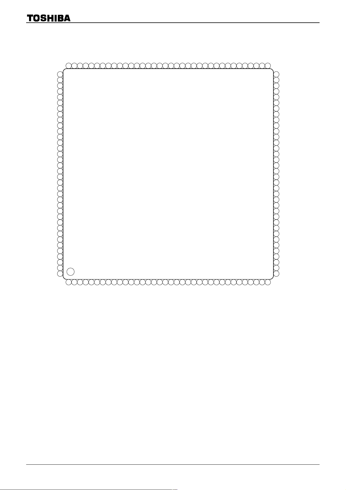
Pin Assignment
Y
Y
TC90A66F
TESO
IICNR
SADSEL
SACN
V
SCL
SDA
TEST4
TEST3
TEST2
TEST1
TEST0
V
T107
T106
T105
T104
T103
T102
T101
T100
CNT6
CNT5
CNT4
CNT3
V
DAV
YOUT
DAV
IOUT
DAV
QOUT
VB2
VB1
VREF
ADBIAS
SS
DD
SS
DD
SS
DD
109
110
111
112
113
114
115
116
117
118
119
120
121
122
123
124
125
126
127
128
129
130
131
132
133
134
135
136
137
138
139
140
141
142
143
144
108
TIMRST
107
PWRST
106
HYOJUN
105
KAYS
YS
104
103
RVD
102
RHD
101
V
DD
100
SS
RMCK
ERRST
EREN
RRST
REN
RDAY7
RDAY6
RDAY5
RDAY4
RCK
RHREF
RMCKI
V
99
98
97
96
95
94
93
92
91
90
RDAY3
89
88
87
86
TC90A66F
RDAY2
DD
RDAY1
RDAY0
V
RDAC7
RDAC6
RDAC5
RDAC4
RDAC3
RDAC2
RDAC1
RDAC0
WDAY0
WDAY1
85
84
83
82
81
80
79
78
77
76
75
74
73
72
WDAY2
71
WDAY3
70
WDAY4
69
WDAY5
68
WDAY6
67
WDAY7
66
V
SS
65
WDAC0
64
WDAC1
63
WDAC2
62
WDAC3
61
WDAC4
60
WDAC5
59
WDAC6
58
WDAC7
57
WRST
56
WEN
55
WIEN
54
EWRST
53
EWEN
52
EWIEN
51
V
SS
50
WMCK
49
V
SS
48
EWMCK
47
V
DD
46
WHREFS
45
WCKS
44
V
SS
43
WHDS
42
WVDS
41
MOH
40
HRST
39
V
DD
38
WHREFE
37
WCKE
1 2 3 4 5 6 7 8 9 10 11 12 13 14 15 16 17 18 19 20 21 22 23 24 25 26 27 28 29 30 31 32 33 34 35 36
SS
DD
IINS
YINS
ADV
ADV
SS
DD
QINS
VRT
VRTC
VRB
ADV
ADV
VRBC
SS
DD
IINE
YINE
ADV
ADV
AV
DD
QINE
AV
SS
DD
V
CNT2
TIN9
TIN8
TIN7
TIN6
TIN5
TIN4
TIN3
TIN2
TIN1
CNT1
CNT0
CLAMP
TIN0
SS
V
WVDE
WHDE
2001-06-07 2
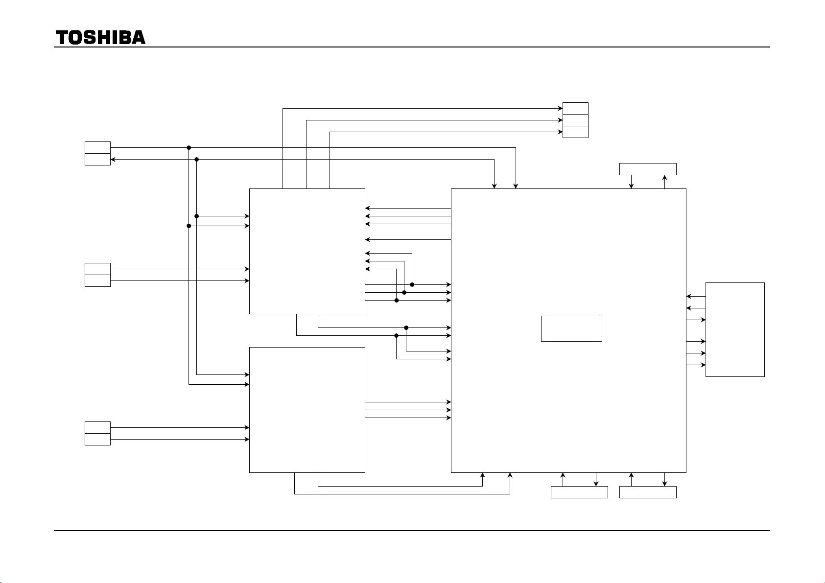
System Block Diagram
Y
K
Y
K
SCL
SDA
µ-COM
TC90A66F
Output signal
Y
I
Q
PLL circuit
YIN
CIN
Sub picture (S)
Image input signal
YIN
CIN
Sub picture (E)
Image input signal
YOUT IOUT QOUT
SDA
SCL
SUB VCD1
TA1270AF
YIN
CIN
HD VD
SDA
SCL
SUB VCD2
TA1270AF
YIN
CIN
HD VD
Y1IN
I1IN
Q1IN
YS
Y2IN
I2IN
Q2IN
YOUT
IOUT
QOUT
YOUT
IOUT
QOUT
SDA SCL
YOUT
IOUT
QOUT
YS
YINS
IINS
QINS
WVDS
WHDS
RVD
RHD
YINE
IINE
QINE
WVDE WHDE WHREFSWCKS
PAP/PIP/POP
TC90A66F
RHREF RCK
WHREFEWCKE
RDA
RDAC
RMC
WDA
WDAC
WMC
2M MEMORY*2
MSM51V8221
PLL circuit
PLL circuit
3
2001-06-07
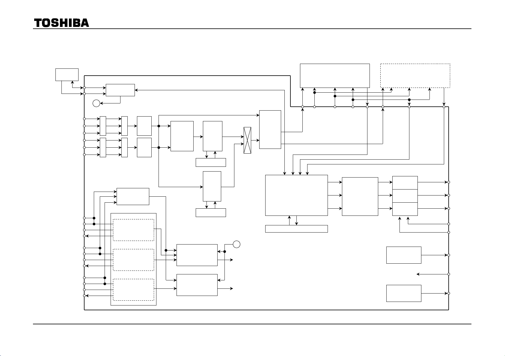
TC90A66F Block Diagram
TC90A66F
(not required in 2M mode)
MAIN
µ-COM
SDA
SCL
YIN (S)
IIN (S)
QIN (S)
YIN (E)
IIN (E)
QIN (E)
Sub picture S
WVDS
WHDS
WCKS
WHREF
Sub picture E
WVDE
WHDE
WCKE
WHREFE
Main picture
RVD
RHD
RCK
RHREF
2M memory
(MSM51V8221)
IN OUT
IIC BUS
A
RMCK
1200 fh
(4M/2M)
WIE
REN
Code processor
C
L
M
P
C
L
M
P
detector circuit
Generates system
clock for write
2400 fh (4M/2M)
Generates system
clock for write
2400 fh (4M/2M)
Generates system
clock for read
2400 fh (4M/2M)
M
A/D
P
X
M
A/D
P
X
Odd/Even
Horizontal
filter
Line memory
Line memory
Generates control
signal for write
Generates control
signal for read
Vertical
filter
Vertical
filter
Y/IQ
separator
Output processor
(frame color select,
Y/C phase adjustment)
Stand processor
A
Control signals for write
Control signals for read
WDAY
7 to 0
WMCK
1200 fh
(4M/2M)
WRST
WENY
WENC
RRST
IN OUT
RDAY
7 to 0
2M memory
(MSM51V8221)
WDAC
7 to 0
D/A
D/A
D/A
Picture display
switch signal
Memory use
switch signal
RMCKI
RDAC
7 to 0
YOUT
IOUT
QOUT
VREF
VB1
VB2
YS
PWRST
MOH
4
2001-06-07

TC90A66F
Pin Functions
Pin
Number
Pin Name I/O Function
1 ADVDD Power supply for A/D (3.3 V)
2 YINS I A/D Y signal (S system) input
3 ADVSS GND for A/D
4 IINS I A/D I signal or R-Y signal (S system) input
5 ADVDD Power supply for A/D (3.3 V)
6 QINS I A/D Q signal or B-Y signal (S system) input
7 ADVSS GND for A/D
8 VRTY I Reference voltage for A/D Y signal (top)
9 VRBY I Reference voltage for A/D Y signal (bottom)
10 VRTC I Reference voltage for A/D I, Q signal (top)
11 VRBC I Reference voltage for A/D I, Q signal (bottom)
12 ADVDD Power supply for A/D (3.3 V)
13 YINE I A/D Y signal (E system) input
14 ADVSS GND for A/D
15 IINE I A/D I signal or R-Y signal (E system) input
16 AVDD Power supply for analog circuit (3.3 V)
17 QINE I A/D Q signal or B-Y signal (E system) input
18 AVSS GND for analog circuit
19 VDD Power supply (3.3 V)
20 CNT2 O Test output pin
21 CNT1 O Test output pin
22 CNT0 O Test output pin
23 CLAMP O Clamp signal monitor output
24 TIN9 I Test input pin (connect to GND)
25 TIN8 I Test input pin (connect to GND)
26 TIN7 I Test input pin (connect to GND)
27 TIN6 I Test input pin (connect to GND)
28 TIN5 I Test input pin (connect to GND)
29 TIN4 I Test input pin (connect to GND)
30 TIN3 I Test input pin (connect to GND)
31 TIN2 I Test input pin (connect to GND)
32 TIN1 I Test input pin (connect to GND)
33 TIN0 I Test input pin (connect to GND)
34 WVDE I (E system) vertical sync signal input (It can be inverted using I2C bus) (Note1)
35 WHDE I (E system) horizontal sync signal input (It can be inverted using I2C bus) (Note1)
36 VSS GND
37 WCKE I (E system) system clock input (Note1)
38 WHREFE I/O (E system) PLL phase comparison output
39 VDD Power supply (3.3 V)
40 HRST O Unit adjusting pin
41 MOH O Memory use switch signal [(YCS (L)㨯TC90A66F (H))
(144-pin QFP)
Note1: Supports 5 V interface.
5
2001-06-07

TC90A66F
Pin
Number
Pin Name I/O Function
42 WVDS I (S system) vertical sync signal input (It can be inverted using I2C bus) (Note1)
43 WHDS I (S system) horizontal sync signal input (It can be inverted using I2C bus) (Note1)
44 VSS GND
45 WCKS I (S system) system clock input (Note1)
46 WHREFS O (S system) PLL phase comparison output
47 VDD Power supply (3.3 V)
48 EWMCK O (E system) write clock output for field memory
49 VSS GND
50 WMCK O (S system) write clock output for field memory
51 VSS GND
52 EWIEN O (E system) field memory input enable
53 EWEN O (E system) field memory write enable
54 EWRST O (E system) field memory write reset
55 WIEN O (S system) field memory input enable
56 WEN O (S system) field memory write enable
57 WRST O (S system) field memory write reset
58 WDAC7 O IQ or sub picture (E system) signal output (field memory write signal/MSB)
59 WDAC6 O IQ or sub picture (E system) signal output (field memory write signal/ : )
60 WDAC5 O IQ or sub picture (E system) signal output (field memory write signal/ : )
61 WDAC4 O IQ or sub picture (E system) signal output (field memory write signal/ : )
62 WDAC3 O IQ or sub picture (E system) signal output (field memory write signal/ : )
63 WDAC2 O IQ or sub picture (E system) signal output (field memory write signal/ : )
64 WDAC1 O IQ or sub picture (E system) signal output (field memory write signal/ : )
65 WDAC0 O IQ or sub picture (E system) signal output (field memory write signal/LSB)
66 VSS GND
67 WDAY7 O Y or sub picture (S system) signal output (field memory write signal/MSB)
68 WDAY6 O Y or sub picture (S system) signal output (field memory write signal/ : )
69 WDAY5 O Y or sub picture (S system) signal output (field memory write signal/ : )
70 WDAY4 O Y or sub picture (S system) signal output (field memory write signal/ : )
71 WDAY3 O Y or sub picture (S system) signal output (field memory write signal/ : )
72 WDAY2 O Y or sub picture (S system) signal output (field memory write signal/ : )
73 WDAY1 O Y or sub picture (S system) signal output (field memory write signal/ : )
74 WDAY0 O Y or sub picture (S system) signal output (field memory write signal/LSB)
75 RDAC0 I IQ or sub picture (E system) signal input (field memory read signal/LSB) (Note1)
76 RDAC1 I IQ or sub picture (E system) signal input (field memory read signal/ : ) (Note1)
77 RDAC2 I IQ or sub picture (E system) signal input (field memory read signal/ : ) (Note1)
78 RDAC3 I IQ or sub picture (E system) signal input (field memory read signal/ : ) (Note1)
79 RDAC4 I IQ or sub picture (E system) signal input (field memory read signal/ : ) (Note1)
80 RDAC5 I IQ or sub picture (E system) signal input (field memory read signal/ : ) (Note1)
81 RDAC6 I IQ or sub picture (E system) signal input (field memory read signal/ : ) (Note1)
82 RDAC7 I IQ or sub picture (E system) signal input (field memory read signal/MSB) (Note1)
83 VDD Power supply (3.3 V)
84 RDAY0 I Y or sub picture (S system) signal input (field memory read signal/LSB) (Note1)
Note1: Supports 5 V interface.
6
2001-06-07
TC90A66F
Pin
Number
Pin Name I/O Function
85 RDAY1 I Y or sub picture (S system) signal input (field memory read signal/ :) (Note1)
86 RDAY2 I Y or sub picture (S system) signal input (field memory read signal/ : ) (Note1)
87 RDAY3 I Y or sub picture (S system) signal input (field memory read signal/ : ) (Note1)
88 RDAY4 I Y or sub picture (S system) signal input (field memory read signal/ : ) (Note1)
89 RDAY5 I Y or sub picture (S system) signal input (field memory read signal/ : ) (Note1)
90 RDAY6 I Y or sub picture (S system) signal input (field memory read signal/ : ) (Note1)
91 RDAY7 I Y or sub picture (S system) signal input (field memory read signal/MSB) (Note1)
92 REN O (S system) field memory read enable
93 RRST O (S system) field memory read reset
94 EREN O (E system) field memory read enable
95 ERRST O (E system) field memory read reset
96 RMCK O (S/E system) read clock output for field memory
97 RMCKI I RMCK input (phase adjustment)
98 VSS GND
99 RHREF O PLL phase comparison output for main picture
100 RCK I System clock input for main picture (Note1)
101 VDD Power supply (3.3 V)
102 RHD I Horizontal sync single input for main picture (It can be inverted using I2C bus) (Note1)
103 RVD I Vertical sync single input for main picture (It can be inverted using I2C bus) (Note1)
104 YS O YS signal output
105 KAYS O Wallpaper YS signal output
106 HYOJUN O Standard/non-standard signal output [standard (L)/non-standard (H)]
107 PWRST I System reset input [reset (L)]
108 TIMRST I Test reset input [reset (H)/normal (L)]
109 TESO O Test monitor output
110 IICNR I I2C bus noise reduction circuit [on (H)/off (L)]
111 SADSEL I Main/sub sub address switch [main (H)/sub (L)]
112 SACN O I2C bus acknowledge output pin
113 VSS GND
114 SCL I I2C bus serial clock input (Note1)
115 SDA I/O I2C bus serial data input (IN)/acknowledge (OUT) (Note1)
116 TEST4 I Test input pin (connect to GND)
117 TEST3 I Test input pin (connect to GND)
118 TEST2 I Test input pin (connect to GND)
119 TEST1 I Test input pin (connect to GND)
120 TEST0 I Test input pin (connect to GND)
121 VDD Power supply (3.3 V)
122 TIO7 I/O Test input/output pin (normally, open)
123 TIO6 I/O Test input/output pin (normally, open)
124 TIO5 I/O Test input/output pin (normally, open)
125 TIO4 I/O Test input/output pin (normally, open)
126 TIO3 I/O Test input/output pin (normally, open)
127 TIO2 I/O Test input/output pin (normally, open)
Note1: Supports 5 V interface.
7
2001-06-07
Pin
Number
Pin Name I/O Function
128 TIO1 I/O Test input/output pin (normally, open)
129 TIO0 I/O Test input/output pin (normally, open)
130 CNT6 O Test output pin
131 CNT5 O Test output pin
132 CNT4 O Test output pin
133 CNT3 O Test output pin
134 VSS GND
135 DAVDD Power supply for D/A (3.3 V)
136 YOUT O Y Signal output
137 DAVSS D/A GND
138 IOUT O I signal or R-Y signal output
139 DAVDD Power supply for D/A (3.3 V)
140 QOUT O Q signal or B-Y signal output
141 VB2 D/A bias
142 VB1 D/A bias
143 VREF I D/A reference bias (supply 2.3 V)
144 ADBIAS A/D bias
TC90A66F
8
2001-06-07
Pin Description
Pin Number Pin Name Function
2 YINS Y-signal (S system) analog input
Input amplitude is 1 V
4 IINS I or R-Y signal (S system) analog input
Input amplitude is 1 V
6 QINS Q or B-Y signal (S system) analog input
Input amplitude is 1 V
8 VRTY High-level reference power supply pin for ADC Y signal. Sets the upper limit of the ADC dynamic
range. Fixed to 2.2 V (typ.) by internal resistance type potential division. Connect 0.1 µF bypass
capacitor between the pin and GND.
9 VRBY Low-level reference power supply voltage for ADC Y signal. Sets the lower limit of the ADC dynamic
range. Fixed to 1.1 V (typ.) by internal resistance type potential division. Connect 0.1 µF bypass
capacitor between the pin and GND.
10 VRTC High-level reference power supply pin for ADC IQ signal. Sets the upper limit of the ADC dynamic
range. Fixed to 2.2 V (typ.) by internal resistance type potential division. Connect 0.1 µF bypass
capacitor between the pin and GND.
11 VRBC Low-level reference power supply voltage for ADC IQ signal. Sets the lower limit of the ADC dynamic
range. Fixed to 1.1 V (typ.) by internal resistance type potential division. Connect 0.1 µF bypass
capacitor between the pin and GND.
13 YINE Y signal (E system) analog input
Input amplitude is 1 V
15 IINE I or R-Y signal (E system) analog input
Input amplitude is 1 V
17 QINE Q or B-Y signal (E system) analog input
Input amplitude is 1 V
23 CLAMP Clamp signal monitor output pin.
Can monitor clamp pulse start/stop position set at 24h or 25h.
Outputs signal for the last data (S or E system) transfer.
34 WVDE (E system) vertical sync signal input pin. (It can be inverted using I2C bus)
Inputs vertical sync signal from VCD for sub picture E. It is composing 5 V interface. For negative
polarity input, set sub address [26H: EVINV] to L (negative polarity input).
35 W HDE (E system) horizontal sync signal input pin. (It can be inverted using I2C bus)
Inputs horizontal sync signal from VCD for sub picture E. It is composing 5 V interface. For negative
polarity input, set sub address [26H: EHINV] to L (negative polarity input).
37 WCKE (E system) write clock input pin. Inputs from the external PLL circuit. It is composing 5 V interface.
Inputs 2400 fH for both 4M and 2M memory mode.
38 WHREFE (E system) PLL phase comparison output.
The HREF signal obtained by the I/N divider circuit or the phase comparison result of sub picture (E)
horizontal sync signal.
40 HRST Unit adjustment (WS/WE/R switch able)
41 MOH External field memory use signal output pin.
Output amplitude is 3.3 V
Setting sub address [21H: MOH] to H uses TC90A66F; setting to L sets all memory output pins to Hi-Z.
42 WVDS (S system) vertical sync signal input pin. (It can be inverted using I2C bus)
Inputs vertical sync signal from VCD for sub picture S. It is composing 5 V interface. For negative
polarity input, set sub address [27H: WVINV] to L (negative polarity input).
43 W HDS (S system) horizontal sync signal input pin. (It can be inverted using I2C bus)
Inputs horizontal sync signal from VCD for sub picture S. It is composing 5 V interface. For negative
polarity input, set sub address [27H: WHINV] to L (negative polarity input).
45 WCKS (S system) write clock input pin. Inputs from the external PLL circuit. It is composing 5 V interface.
Inputs 2400 fH for both 4M and 2M memory mode.
typical.
p-p
typical.
p-p
typical.
p-p
typical.
p-p
typical.
p-p
typical.
p-p
typical.
p-p
TC90A66F
9
2001-06-07

Pin Number Pin Name Function
46 WHREFS (S system) PLL phase comparison output.
The HREF signal obtained by the I/N divider circuit or the phase comparison result of sub picture (S)
horizontal sync signal. This signal is used to control the external VCO voltage.
48 EWMCK Outputs sub picture E write clock to external field memory.
Output amplitude is 3.3 V
typical.
p-p
50 WMCK Outputs sub picture S write clock to external field memory.
Output amplitude is 3.3 V
typical.
p-p
52 EWIEN Control signal output pin for external field memory (sub picture E).
Output amplitude is 3.3 V
typical.
p-p
53 EWEN Control signal output pin for external field memory (sub picture E).
Output amplitude is 3.3 V
typical.
p-p
54 EWRST Control signal output pin for external field memory (sub picture E).
Output amplitude is 3.3 V
typical.
p-p
55 WIEN Control signal output pin for external field memory (sub picture S).
Output amplitude is 3.3 V
typical.
p-p
56 WEN Control signal output pin for external field memory (sub picture S).
Output amplitude is 3.3 V
typical.
p-p
57 WRST Control signal output pin for external field memory (sub picture S).
Output amplitude is 3.3 V
typical.
p-p
58 to 65 WDAC7-0 Output signal to write to external field memory. (I, Q or E system).
Output amplitude is 3.3 V
typical.
p-p
Connect only when using 4M memory.
MSB: WDAC7, LSB: WDAC0
67 to 75 WDAY7-0 Output signal to write to external field memory. (Y or S system).
Output amplitude is 3.3 V
typical.
p-p
MSB: WDAY7, LSB: WDAY0
75 to 82 RDAC0-7 Input signal to read from external field memory (I, Q or E system).
It is composing 5 V interface.
Connect only when using 4M memory.
MSB: RDAC7, LSB: RDAC0
84 to 91 RDAY0-7 Input signal to read from external field memory (Y or S system).
It is composing 5 V interface.
MSB: RDAY7, LSB: RDAY0
92 REN Control signal output pin for external field memory (sub picture S).
Output amplitude is 3.3 V
typical.
p-p
93 RRST Control signal output pin for external field memory (sub picture S).
Output amplitude is 3.3 V
typical.
p-p
94 EREN Control signal output pin for external field memory (sub picture E).
Output amplitude is 3.3 V
typical.
p-p
95 ERRST Control signal output pin for external field memory (sub picture E).
Output amplitude is 3.3 V
typical.
p-p
96 RMCK Outputs read clock to external field memory.
Output amplitude is 3.3 V
typical.
p-p
Outputs 1200 fH for both 4M and 2M memory.
97 RMCKI RMCK phase adjustment input pin. Inputs RMCK.
TC90A66F
10
2001-06-07
Pin Number Pin Name Function
99 RHREF PLL phase compare output pin for main picture.
The HREF signal obtained by the I/N divider circuit or the phase comparison result of RHD signal. This
signal is used to control the external VCO voltage.
100 RCK Read clock input pin. It is composing 5 V interface.
Inputs from the external PLL circuit.
Inputs 2400 fH for both 4M and 2M memory.
102 RHD Horizontal sync signal input pin for main picture (read). Inputs horizontal sync signal from VCD for main
picture. It is composing 5 V interface (negative polarity input). For negative polarity input, set sub
address [28H: RHINV] to non-inversion (L).
103 RVD Vertical sync signal input pin for main picture (read). Inputs vertical sync signal from VCD for main
picture. It is composing 5 V interface (negative polarity input). For negative polarity input, set sub
address [28H: RVINV] to non-inversion (L).
104 YS Main/sub picture switch timing signal output pin. Output amplitude is 3.3 V
signal is High, displays sub picture.
105 KAYS Wallpaper YS signal output.
106 HYOJUN Standard/non-standard signal output pin [standard (L)/non-standard (H)]
107 PWRST System reset input pin. When low input, it carries out the reset.
At least 1 V is required as reset duration.
110 IICNR I2C bus noise reduction circuit setting pin.
When set to on (connect to V
When set to off (connect to GND), data are written to register directly.
111 SADSEL Sub address of main/sub picture switching pin. [main (H)/sub (L)]
Normally, set to L (enables sub addresses 00h to 7Fh).
112 SACN I2C bus acknowledge output pin.
114 SCL I2C bus serial clock input pin. It is composing 5 V interface.
115 SDA I2C bus serial data input/acknowledge output pin.
It is composing 5 V interface.
136 YOUT Y signal output pin. Output amplitude is 0.9 V
138 IOUT I signal output pin. Output amplitude is 0.9 V
140 QOUT Q signal output pin. Output amplitude is 0.9 V
141 to 142 VB2-1 Bias pin for DAC.
Connect a 0.1 µF bypass capacitor between the pins and GND.
143 VREF DAC reference voltage input pin.
Reference voltage is 2.3 V typical.
144 ADBIAS Bias pin for ADC.
Connect a 0.1 µF bypass capacitor between the pin and AGND.
), data are latched once by the internal clock, then written to register.
DD
typical.
p-p
typical.
p-p
typical.
p-p
typical. When the YS
p-p
TC90A66F
11
2001-06-07
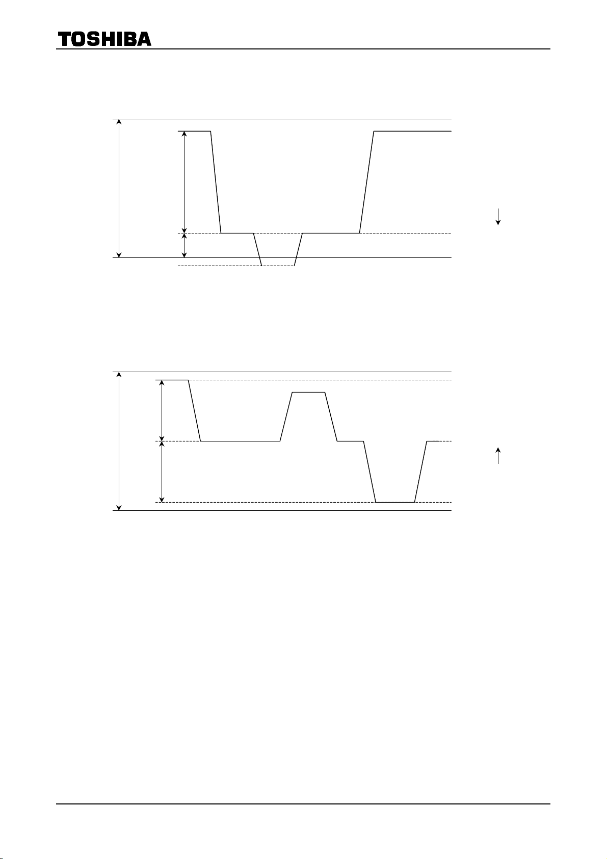
Example of Typical A/D Converter Input Level for Luminance Signal
2.2 V
100 (IRE)
TC90A66F
Dec. HEX
255
FFH
228
E4H
1.1 V
1.1 V
0.71 V
0 (IRE)
0.27 V
−40 (IRE)
signal amplitude: 1.0 V
(100% white)
p-p
pedestal clamp value
Example of Typical A/D Converter Input Level for Chrominance Signal
2.2 V
0.5 V
1.1 V
0.5 V
reference potential
clamp value
63
3FH
0
00H
Dec. HEX
255
FFH
251
EBH
136 88H
21
15H
0
1.1 V
signal amplitude: 1.0 V
p-p
00H
12
2001-06-07

Example of Typical D/A Converter Output Level for Luminance Signal
Dec. HEX
3.3 V
100 (IRE)
TC90A66F
255
FFH
228
E4H
1.0 V
2.3 V
0.64 V
0 (IRE)
0.25 V
−40 (IRE)
signal amplitude: 0.9 V
(100% white)
p-p
63
0
Example of Typical D/A Converter Output Level for Chrominance Signal
Dec. HEX
255
243
128 80H
1.1 V
3.3 V
3.25 V
0.45 V
2.8 V
0.45 V
3FH
00H
FFH
E3H
2.3 V
2.35 V
signal amplitude: 0.9 V
p-p
13
0
0DH
00H
13
2001-06-07

Picture Display Function
TC90A66F
Sub picture (S) Main picture (E)
2-picture (PAP) display
4:3 aspect ratio (full picture can be displayed)
sub picture (S), (E): motion or still
(pictures can be exchanged)
Sub picture (S)
Multi search pictures
Sub picture (S): motion or still
Sub picture (E): 9 or 12 still pictures, strobe display or
only 1 motion picture and others still.
picture
Main picture
3-picture POP display
Sub picture: 4:3 aspect ratio Still, strobe, only 1
motion picture
Main picture: display using TC90A18AF (EDWAC)
picture
picture
sub
(S)
sub
(S)
sub
(S)
Sub picture (S)
1-picture display
(full picture can be used)
Main picture
sub
picture
(S)
PIP display
Sub picture: 16:9 or 4:3 aspect ratio
Motion or still
Main picture: display using TC90A18AF (EDWAC)
Multiple picture search using the whole screen
12 or 9 still pictures, strobe display,
only 1 motion picture and others still
14
2001-06-07

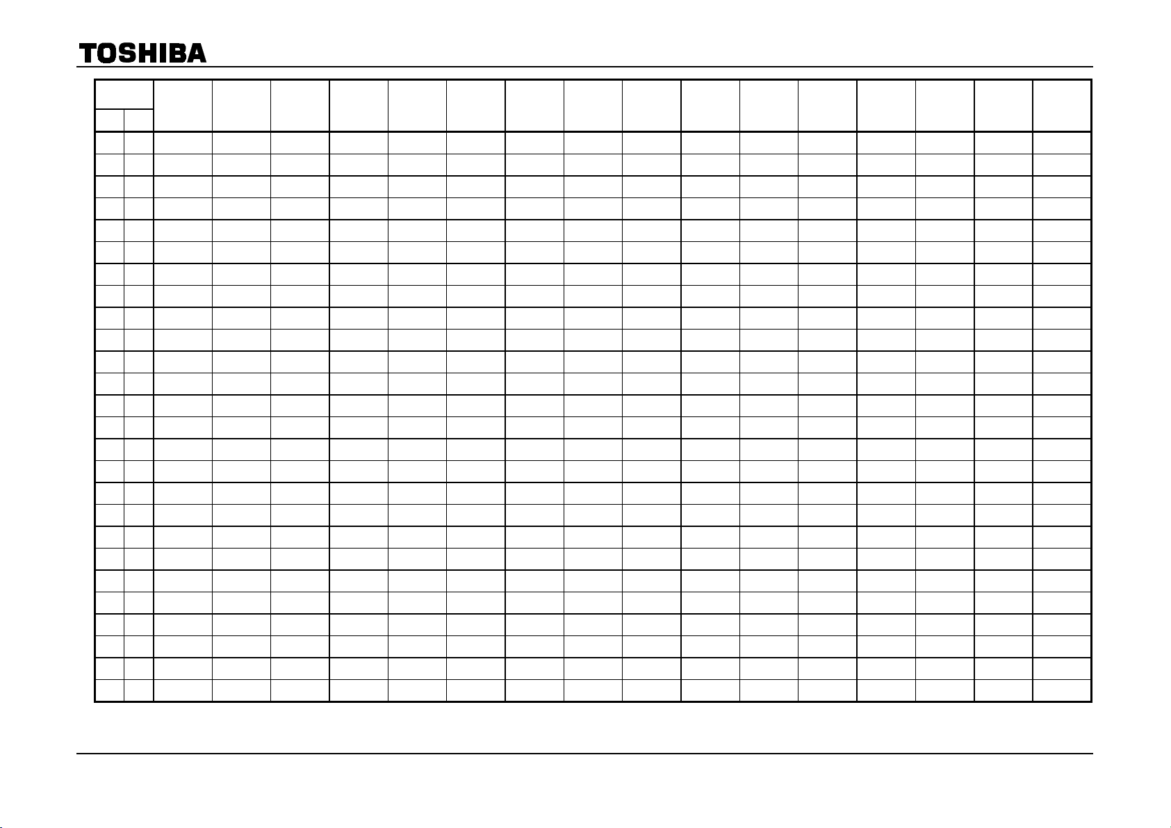
I2C Bus Address Setting Table
TC90A66F
Sub
Address
䌈䌥䌸 Dec 15 14 13 12 11 10 9 8 7 6 5 4 3 2 1 0
00 0 MYPH2 → 1 → 0 MYQPH0 RRSTINV RCKINV RREPH1 → 0 M4M2 SESW
01 1 YSBACT FRACLR YSCCLR YSBCLR YSACLR
02 2 MBLKIQ7 → 6 → 5 → 4 → 3 → 2 → 1 → 0 MBLKY7 → 6 → 5 → 4 → 3 → 2 → 1 → 0
03 3 MMW IQ7 → 6 → 5 → 4 → 3 → 2 → 1 → 0 MMWY7 → 6 → 5 → 4 → 3 → 2 → 1 → 0
04 4
05 5
06 6
07 7
08 8
09 9
0A 10
0B 11
0C 12
0D 13
0E 14
0F 15
10 16
11 17
12 18
13 19
14 20
15 21 RHSIZ11 → 10 → 9 → 8 → 7 → 6 → 5 → 4 → 3 → 2 → 1 → 0
16 22 RVSIZ9 → 8 → 7 → 6 → 5 → 4 → 3 → 2 → 1 → 0
17 23 ROEFON RGAME DWSW RRH11 → 10 → 9 → 8 → 7 → 6 → 5 → 4 → 3 → 2 → 1 → 0
18 24 FRFI ROEALT RFISW RFALT RRV9 → 8 → 7 → 6 → 5 → 4 → 3 → 2 → 1 → 0
MSB
RHYSAE11
RHYSAS11
RHYSBE11
RHYSBS11
RHYSCE11
RHYSCS11 → 10 → 9 → 8 → 7 → 6 → 5 → 4 → 3 → 2 → 1 → 0
→ 10 → 9 → 8 → 7 → 6 → 5 → 4 → 3 → 2 → 1 → 0
→ 10 → 9 → 8 → 7 → 6 → 5 → 4 → 3 → 2 → 1 → 0
RVYSAE9
RVYSAS9
→ 10 → 9 → 8 → 7 → 6 → 5 → 4 → 3 → 2 → 1 → 0
→ 10 → 9 → 8 → 7 → 6 → 5 → 4 → 3 → 2 → 1 → 0
RVYSBE9
RVYSBS9
→ 10 → 9 → 8 → 7 → 6 → 5 → 4 → 3 → 2 → 1 → 0
RVYSCE9
RVYSCS9
→ 8 → 7 → 6 → 5 → 4 → 3 → 2 → 1 → 0
→ 8 → 7 → 6 → 5 → 4 → 3 → 2 → 1 → 0
→ 8 → 7 → 6 → 5 → 4 → 3 → 2 → 1 → 0
→ 8 → 7 → 6 → 5 → 4 → 3 → 2 → 1 → 0
→ 8 → 7 → 6 → 5 → 4 → 3 → 2 → 1 → 0
→ 8 → 7 → 6 → 5 → 4 → 3 → 2 → 1 → 0
LSB
Note2: Set 0 in blank columns.
15
2001-06-07

TC90A66F
Sub
Address
䌈䌥䌸 Dec 15 14 13 12 11 10 9 8 7 6 5 4 3 2 1 0
19 25 RWRN9 → 8 → 7 → 6 → 5 → 4 → 3 → 2 → 1 → 0
1A 26 RWRA9 → 8 → 7 → 6 → 5 → 4 → 3 → 2 → 1 → 0
1B 27 RHRFTH RHRFIV RHINV2 RCKCHG PRHP11 → 10 → 9 → 8 → 7 → 6 → 5 → 4 → 3 → 2 → 1 → 0
1C 28
1D 29 DWFIL JSWAP WHST10 → 9 → 8 → 7 → 6 → 5 → 4 → 3 → 2 → 1 → 0
1E 30 WHMOD3 → 2 → 1 → 0 WCKINV WHED10 → 9 → 8 → 7 → 6 → 5 → 4 → 3 → 2 → 1 → 0
1F 31 WEYINV WEYDL2 → 1 IENINV KWST10 → 9 → 8 → 7 → 6 → 5 → 4 → 3 → 2 → 1 → 0
20 32 WECINV WECDL2 → 1 → 0 WEPCM KWED10 → 9 → 8 → 7 → 6 → 5 → 4 → 3 → 2 → 1 → 0
21 33 WHRFTH WHRFIV WHINV2 MOH SHRST11 → 10 → 9 → 8 → 7 → 6 → 5 → 4 → 3 → 2 → 1 → 0
22 34 PCMAIN SIQINV EIQINV EHRST11 → 10 → 9 → 8 → 7 → 6 → 5 → 4 → 3 → 2 → 1 → 0
23 35 WCKEON PHREF11 → 10 → 9 → 8 → 7 → 6 → 5 → 4 → 3 → 2 → 1 → 0
24 36 SCLPST7 → 6 → 5 → 4 → 3 → 2 → 1 → 0
25 37 ECLPST7 → 6 → 5 → 4 → 3 → 2 → 1 → 0
26 38 W PLHS EPLHS EHINV EVINV NTPAL RPLHS HDWDT7 → 6 → 5 → 4 → 3 → 2 → 1
27 39 WHIHYO WKHYO WHINV WVINV WS262 HYJ3 → 2 → 1 WVMSK7 → 6 → 5 → 4 → 3
28 40 RHIHYO RKHYO RHINV RVINV RS262 HIJ3 → 2 → 1 RVMSK7 → 6 → 5 → 4 → 3 → 2 → 1 → 0
29 41
2A 42 JWRTON POEINV INT3S2 RSTDEL WVED8 → 7 → 6 → 5 → 4 → 3 → 2 → 1 → 0
2B 43 FIELD VSPD1 → 0 JVSCRL VL8 → 7 → 6 → 5 → 4 → 3 → 2 → 1 → 0
2C 44 MWBACK BVIE5 → 4 → 3 → 2 → 1 → 0 BVW E8 → 7 → 6 → 5 → 4 → 3 → 2 → 1 → 0
2D 45 MULT STREND VSKOFF KSKOFF RANDM HIE9 → 8 → 7 → 6 → 5 → 4 → 3 → 2 → 1 → 0
2E 46 BHIE5 → 4 → 3 → 2 → 1 → 0 KJH9 → 8 → 7 → 6 → 5 → 4 → 3 → 2 → 1 → 0
2F 47 BVRN3 → 2 → 1 → 0 BHRN3 → 2 → 1 → 0 KJV7 → 6 → 5 → 4 → 3 → 2 → 1 → 0
30 48 ATMV3 → 2 → 1 → 0 ATMH3 → 2 → 1 → 0 ATFLD7 → 6 → 5 → 4 → 3 → 2 → 1 → 0
31 49 STMV3 → 2 → 1 → 0 STMH3 → 2 → 1 → 0 STVS7 → 6 → 5 → 4 → 3 → 2 → 1 → 0
32 50 ATSTRV ATSTRH AT2CHG STHS9 → 8 → 7 → 6 → 5 → 4 → 3 → 2 → 1 → 0
MSB
JVLOCHG
RPLLPH11
JFMINT JVLOINV W KYFRM MAINRST MSKOFF VFILOFF WVST8 → 7 → 6 → 5 → 4 → 3 → 2 → 1 → 0
→ 10 → 9 → 8 → 7 → 6 → 5 → 4 → 3 → 2 → 1 → 0
SCLPED7
ECLPED7
→ 6 → 5 → 4 → 3 → 2 → 1 → 0
→ 6 → 5 → 4 → 3 → 2 → 1 → 0
WOERSTN
EHIHYO EKHYO
LSB
Note2: Set 0 in blank columns.
16
2001-06-07

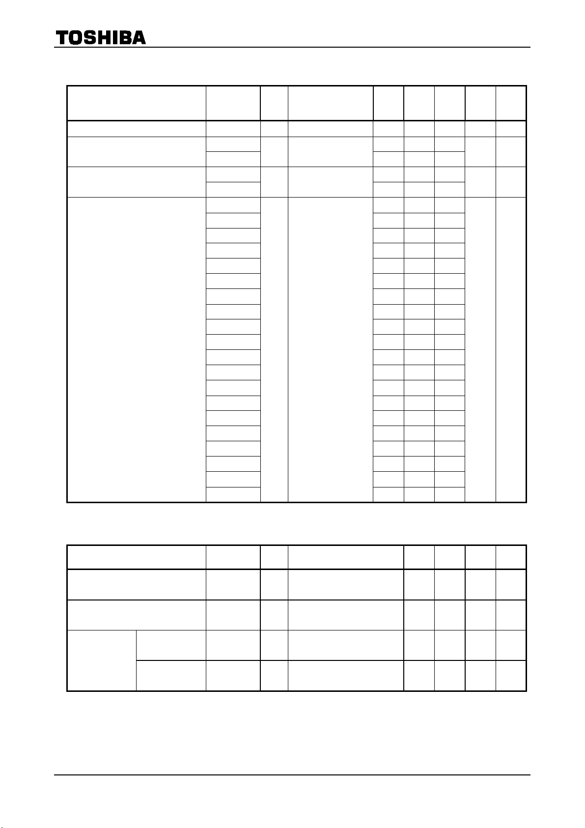
TC90A66F
Sub
Address
䌈䌥䌸 Dec 15 14 13 12 11 10 9 8 7 6 5 4 3 2 1 0
33 51 CHMV3 → 2 → 1 → 0 CHMH3 → 2 → 1 → 0 ATLV3 → 2 → 1 → 0 ATLH3 → 2 → 1 → 0
34 52 RH9 → 8 → 7 → 6 → 5 → 4 → 3 → 2 → 1 → 0
35 53 YCMF2 YCMF1 YCMN C2HFT Y2HFT W1NSEL THRUY KMODE THRUYC YDL2 → 1 → 0 KTC KTB KTA OFSET
36 54 KD15 → 14 → 13 → 12 → 11 → 10 → 9 → 8 → 7 → 6 → 5 → 4 → 3 → 2 → 1 → 0
37 55 KD31 → 30 → 29 → 28 → 27 → 26 → 25 → 24 → 23 → 22 → 21 → 20 → 19 → 18 → 17 → 16
38 56 HFSPAIV YLPFCH THRUC CLPFTH YLPFTH
39 57 VFN3 → 2 → 1 → 0 VFYTH VKOS4 → 3 → 2 → 1 → 0
3A 58
3B 59 SYCINV PCMAIN STHRU
3C 60
3D 61
3E 62
3F 63
40 64 FRAON
41 65
42 66
43 67
44 68
45 69
46 70
47 71
48 72
49 73
4A 74
4B 75
4C 76
MSB
BMASKON
CBYS ABYS ACYS
LSB
Note2: Set 0 in blank columns.
17
2001-06-07
TC90A66F
Sub
Address
䌈䌥䌸 Dec 15 14 13 12 11 10 9 8 7 6 5 4 3 2 1 0
4D 77
4E 78
4F 79
50 80
51 81
52 82
53 83
54 84
55 85
56 86
57 87
58 88
59 89
5A 90
5B 91
5C 92
5D 93
5E 94
5F 95
60 96
61 97 MFRAIQ7 → 6 → 5 → 4 → 3 → 2 → 1 → 0 MFRAY7 → 6 → 5 → 4 → 3 → 2 → 1 → 0
62 98
63 99
64 100
65 101
66 102
MSB
RHMBLE11
RHMBLS11
RMHCNT11
→ 10 → 9 → 8 → 7 → 6 → 5 → 4 → 3 → 2 → 1 → 0
→ 10 → 9 → 8 → 7 → 6 → 5 → 4 → 3 → 2 → 1 → 0
RVMBLE9
RVMBLS9
→ 10 → 9 → 8 → 7 → 6 → 5 → 4 → 3 → 2 → 1 → 0
RMVCNT9
RMHTES10
→ 9 → 8 → 7 → 6 → 5 → 4 → 3 → 2 → 1 → 0
→ 8 → 7 → 6 → 5 → 4 → 3 → 2 → 1 → 0
→ 8 → 7 → 6 → 5 → 4 → 3 → 2 → 1 → 0
→ 8 → 7 → 6 → 5 → 4 → 3 → 2 → 1 → 0
LSB
Note2: Set 0 in blank columns.
18
2001-06-07

TC90A66F
Sub
Address
䌈䌥䌸 Dec 15 14 13 12 11 10 9 8 7 6 5 4 3 2 1 0
67 103
68 104
69 105 RMWSEL
6A 106
6B 107 FHWE3 → 2 → 1 → 0 RHFRE11 → 10 → 9 → 8 → 7 → 6 → 5 → 4 → 3 → 2 → 1 → 0
6C 108 FHWS3 → 2 → 1 → 0 RHFRS11 → 10 → 9 → 8 → 7 → 6 → 5 → 4 → 3 → 2 → 1 → 0
6D 109 FVWE3 → 2 → 1 → 0 FHEON FHSON RVFRE9 → 8 → 7 → 6 → 5 → 4 → 3 → 2 → 1 → 0
6E 110 FVWS3 → 2 → 1 → 0 FVEON FVSON RVFRS9 → 8 → 7 → 6 → 5 → 4 → 3 → 2 → 1 → 0
6F 111
70 112
71 113
72 114
73 115
74 116
75 117
76 118
77 119
78 120
79 121
7A 122
7B 123
7F 127 AUTOIN
MSB
YSCMVON
RMVTES8 → 7 → 6 → 5 → 4 → 3 → 2 → 1 → 0
→ 5 → 4 → 3 → 2 → 1 → 0
RMHSEL4
→ 3 → 2 → 1
YSAMVON YSBMVON
RHMDN RMHUP
RMVSEL4
RMHMOV6
RMVMOV6 → 5 → 4 → 3 → 2 → 1 → 0
→ 3 → 2 → 1
LSB
Note2: Set 0 in blank columns.
19
2001-06-07
TC90A66F
Outline of I2C Bus Control Format
I2C bus control for the TC90A31F conforms to the Philips format.
Data Transfer Format
S Slave address 0 A Sub address A XXXXXXXX A XXXXXXXX A P
7-bit 8-bit 8-bit
MSB MSB MSB
S: start condition
P: stop condition
A: acknowledge
(1) Start and stop conditions
SDA
SCL
S
Start condition
when clock line = H,
defined at the falling
edge of data line.
(2) Bit transfer
8-bit
MSB
P
Stop condition
When clock line = H,
defined at the rising
edge of data line.
SDA
SCL
SDA may be changed. Do not change SDA.
Data are valid only when
clock pulse = H (including
rising/falling edges).
20
2001-06-07

TC90A66F
r
(3) Acknowledge
SDA from maste
SDA from slave
SCL from master
S
High impedance
(4) Slave address
A6 A5 A4 A3 A2 A1 A0 R/W
0 0 1 0 0 1 1 0
Purchase of TOSHIBA I
components in an I
2
2
C components conveys a license under the Philips I2C Patent Right to use these
C system, provided that the system conforms to the I2C
Standard Specification as defined by Philips.
High impedance
8 1
9
21
2001-06-07

TC90A66F
I2C Bus Functions
Sub
Address
Hex Dec
1D 29 15 DWFIL Image compression switching PAP (L) image compression (H)
14 JSWAP Memory write control S/E inversion inversion (H) (used at right-and-left picture swapping)
10-0 WHST10-0 Horizontal write start position
1E 30 15-12 WHMOD3-0 Horizontal reduction ratio
1/16 (0H) 1/8 (1H) 1/5 (2H) 1/4 (3H) 1/3 (4H) 3/8 (5H)
2/5 (6H) 1/2 (7H) 3/5 (8H) 5/8 (9H) 2/3 (AH) 3/4 (BH)
4/5 (CH) 7/8 (CH) 15/16 (EH) 16/16 (FH)
11 WCKINV Memory WCK phase inversion inversion (H)
10-0 WHED10-0 Horizontal write stop position
1F 31 15 WEYINV Memory Y-signal WE polarity inversion polarity inversion (H)
13-12 WEYDL1-0 Memory Y-signal W E delay adjustment
delay 0 (0) delay 1 (1) delay 2 (2) delay-1 (3)
11 IENINV Memory IE polarity inversion polarity inversion (H)
10-0 KWST10-0 Horizontal filter processing start position
20 32 15 WECINV Memory C-signal WE polarity inversion polarity inversion (H)
14 WECDL2 normal (L) when 2M memory mode H3/4 (WHMOD3-0 = BH) is set (H)
13-12 WECDL1-0 Memory C-signal WE delay adjustment
delay 0 (0) delay 1 (1) delay 2 (2) delay-1 (3)
11 WEPCM Memory W E for 1-picture 1-picture processing (H)
10-0 KWED10-0 Horizontal filter processing stop position
21 33 15 W HRFTH HREF signal through function phase comparison (L) through (H)
14 WHRFIV Polarity inversion of HREF signal polarity inversion (H)
13 W HINV2 Polarity inversion of HD signal for phase comparison polarity inversion (H)
12 MOH Field memory use signal YCS (L) PAP IC (H)
11-0 SHRST11-0 S-system horizontal phase reference
22 34 15 PCMAIN 1-picture processing 1-picture processing (H)
14 SIQINV 2M memory S system/4M memory-I/Q inversion I/Q inversion (H)
13 EIQINV 2M memory E system-I/Q inversion I/Q inversion (H)
11-0 EHRST11-0 E-system horizontal phase reference
23 35 12 W CKEON E-system operating control E-system operation (H)
11-0 PHREF11-0 PLL divider counter cycle for write NTSC4M/2M [95D]
24 36 15-8 SCLPST7-0 S-system clamp pulse start position
7-0 SCLPED7-0 S-system clamp pulse stop position (start setting value < stop setting value)
25 37 15-8 ECLPST7-0 E-system clamp pulse start position
7-0 ECLPED7-0 E-system clamp pulse stop position (start setting value < stop setting value)
26 38 15 WPLHS Through function for S-system phase comparison HD signal through (H)
14 EPLHS Through function for E-system phase comparison HD signal through (H)
13 EHINV E-system HD polarity inversion at negative polarity input (L) polarity inversion (H)
12 EVINV E-system VD polarity inversion at negative polarity input (L) polarity inversion (H)
11 NTPAL NTSC/PAL switching for typical detector circuit NTSC (L) PAL (H)
7 RPLHS Through function for phase comparison HD signal for read through (H)
Data Signal Name Function
6-0 HDWDT7-1 Pulse width adjustment function for phase comparison HD signal for read
(write)
(change in units of W1CK)
22
2001-06-07

TC90A66F
Sub
Address
Hex Dec
27 39 15 WHIHYO S-system forced non-standard forced non-standard (H)
14 WKHYO S-system forced standard forced standard (H)
13 WHINV S-system HD signal polarity inversion at negative polarity input (L) polarity inversion (H)
12 WVINV S-system VD signal polarity inversion at negative polarity input (L) polarity inversion (H)
11 WS262 S/E-system odd/even inversion 263 (L) 262 (H)
10-8 HYJ3-1 Read S/E-system standard inversion slice level
7-3 WVMSK7-3 S/E-system VD masking (each 16 lines)
2 WOERSTN Odd/even generator circuit clear stop
1 EHIHYO E-system forced non-standard forced non-standard (H)
0 EKHYO E-system forced standard forced standard (H)
28 40 15 RHIHYO Forced non-standard for read forced non-standard (H)
14 RKHYO Forced standard for read forced standard (H)
11 RS262 Odd/even inversion for read 263 (L) 262 (H)
10-8 HIJ3-1 S/E-system non-standard decision inversion slice level for read
7-0 RVMSK7-0 VD masking for read (each two lines)
29 41 15 JVLOCHG Change of vertical reduction center center of gravity change (H)
14 JFMINT Field memory initialize initialize (H)
13 JVLOINV Change of vertical reduction center direction normal (H)
12 WKYFRM Forced frame write processing forced frame (H)
11 MAINRST Memory reset switching at 1-picture processing 1-picture processing (H)
10 MSKOFF VD masking function off during WE VD mask off (H)
9 VFILOFF Fixed to L
8-0 WVST8-0 Vertical write start line
2A 42 15 JWRTON Write on/off still (L) live (H)
14 POEINV Fixed to L
13 INT3S2 Memory initialize width change 3V (L) 2V (H)
9 RSTDEL Fixed to L
8-0 WVED8-0 Vertical write stop line
2B 43 15 FIELD Only 1-field write 1-field (H)
14-13 VSPD1-0 Scroll down speed change
12 JVSCRL Scroll down on/off off (L) on (H)
8-0 VL8-0 Number of lines to be moved for vertical reduction center normal [001H]
2C 44 15 MWBACK Background on/off off (L) on (H)
14-9 BVIE5-0 [2CH: MWBACK = 1] block vertical interval
8-0 BVWE8-0 [2CH: MWBACK = 1] number of block lines
Data Signal Name Function
13 RHINV Horizontal direction (HD) signal polarity inversion for read
at negative polarity input (L) polarity inversion (H)
12 RVINV Vertical direction (VD) signal polarity inversion for read
at negative polarity input (L) polarity inversion (H)
23
2001-06-07

TC90A66F
Sub
Address
Hex Dec
2D 45 15 MULT Multi-search strobe function on/off on (H)
14 STREND Fixed to L
13 VSKOFF [2DH: MULT = 1] write block position change function on (L) off (H)
12 KSKOFF [2DH: MULT = 1] reference skip function off on (L) off (H)
10 RANDM Fixed to L
9-0 HIE9-0 [2DH: MULT = 1] horizontal skip width
[2CH: MWBACK = 1] number of block pixels
2E 46 15-10 BHIE5-0 [2CH: MWBACK = 1] block horizontal interval
9-0 KJH9-0 [2DH: KSKOFF = 0] reference skip horizontal position
2F 47 15-12 BVRN3-0 [2CH: MWBACK = 1] number of vertical blocks (setting value: number of vertical blocks − 1)
7-0 KJV7-0 [2DH: KSKOFF = 0] reference skip vertical position
30 48 15-12 ATMV3-0 Number of strobe mode vertical blocks (setting value: number of vertical blocks − 1)
11-8 ATMH3-0 Number of strobe mode horizontal blocks (setting value: number of horizontal blocks − 1)
7-0 ATFLD7-0 [2DH: MULT = 1] write field interval (00H = 2Fi, 01H = 4Fi㨯㨯㨯)
31 49 15-12 STMV3-0 [2DH: MULT = 1] vertical block position for 1 motion picture (specified block − 1)
11-8 STMH3-0 [2DH: MULT = 1] horizontal block position for 1 motion picture (specified block − 1)
7-0 STVS7-0 [2DH: MULT = 1] number of vertical block lines
32 50 13 ATSTRV [2DH: MULT = 1] vertical strobe function multi search (L) strobe (H)
12 ATSTRH [2DH: MULT = 1] horizontal strobe function multi search (L) strobe (H)
11 AT2CHG [2DH: MULT = 1] strobe vertical 2-row write function on (H)
9-0 STHS9-0 [2DH: MULT = 1] number of horizontal block pixels (setting value: number of block pixels − 3)
33 51 15-12 CHMV3-0 [32H: AT2CHG = 1] strobe row 2
11-8 CHMH3-0 [32H: AT2CHG = 1] strobe line 2
7-4 ATLV3-0 [32H: AT2CHG = 1] strobe row 1
3-0 ATLH3-0 [32H: AT2CHG = 1] strobe line 1
34 52 9-0 RH9-0 [2DH: MULT = 1] number of multi search horizontal pixels (setting value: horizontal pixels − 3)
= 15H: field memory horizontal read size
In Multi Search, Strobe mode
Number of pixels = (number of block pixels) × (number of horizontal blocks)
35 53 15 YCMF2 YCMIX signal (M/N type) polarity inversion polarity inversion (H)
14 YCMF1 YCMIX signal (before multiplier) polarity inversion polarity inversion (H)
13 YCMN Compression switching M/N compression (L) 1/N compression (H)
12 C2HFT Color signal (I/Q) binary interpolation circuit on/off on (H)
11 Y2HFT Luminance signal binary interpolation circuit on/off on (H)
10 W1NSEL Reduction processor circuit switching M/N (L) 1/N (H)
9 THRUY Through output on/off for Y-signal only on (H)
8 KMODE Horizontal filter coefficient mode switching 1/N processing (L) M/N processing (H)
7 THRUYC [35H: YCMN = 1] horizontal filter through on/off on (H)
6-4 YDL2-0 Y signal delay adjustment
3-1 KTC-A Number of filter coefficients 0Hex = 1, 1Hex = 2,㨯㨯㨯7Hex = 8
0 OFSET Fixed to L
Data Signal Name Function
When set to off, only one picture (upper left) of strobe mode is motion picture. (effective for
ATSTRV, H = 1)
11-8 BHRN3-0 [2CH: MWBACK = 1] number of horizontal blocks
(setting value: number of horizontal blocks − 1)
24
2001-06-07

TC90A66F
Sub
Address
Hex Dec
36 54 15-0 KD15-0 Horizontal filter coefficient 1 (KD 3-0)~coefficient 8 (KD31-28)
37 55 15-0 KD31-16 1/N compression: 10H-setting value (complement) M/N compression: Hex
38 56 7 HFSPAIV [4M mode] polarity inversion of Y/C separation control signal before HFIL stage
3 YLPFCH LPF for Y signal switching Stage 2 (L) stage 1 (H)
2 THRUC C-signal-only through output on/off on (H)
1 CLPFTH LPF for C signal on/off on (H)
0 YLPFTH LPF for Y signal on/off on (H)
39 57 11-8 VFN3-0 Vertical compression ratio (setting value: denominator – 1)
(1/2 → 1, 1/3 → 2, 1/4 → 3, 3/4 → 3, 1/5 −4, 1/6 → 5, 1/8 → 7)
Select from the above reduction ratios.
5 VFYTH Vertical filter through on/off on (H)
4-0 VKOS4-0 RAM address specification for vertical filter coefficient
Set according to the specified vertical reduction ratio as follows:
1/3 (00H), 1/4 (03H), 1/2 (07H), 3/4 (09H), 5/6 (0DH), 1/8 (13H), 1/5 (1BH)
3B 59 11 SYCINV Polarity inversion of Y/C separation control signal polarity inversion (H)
10 PCMAIN 1-picture processing 1-picture processing (H)
8 STHRU SEL block through on/off on (H)
7F 127 8 AUTOIN Vertical filter SRAM data transmission Auto Increment mode [H]
Set to L for no vertical reduction.
Data Signal Name Function
polarity inversion (H)
25
2001-06-07

TC90A66F
I2C Bus Functions
Sub
Address
Hex Dec
00 00 15-13 MYPH2-0 Y signal phase adjustment for read
12 MIQPH0 I/Q signal phase adjustment for read
11 RRSTINV Polarity inversion of field memory read reset (RRST) signal inversion (H)
10 RCKINV Polarity inversion of field memory read clock (PCK) signal inversion (H)
9-8 RREPH1-0 Phase adjustment of field memory read enable (RRE) signal inversion (H)
7 M4M2 4M memory/2M memory mode switching 4M (L) 2M (H)
6 SESW S/E system control switching S system (L) E system (H)
01 01 13 YSBACT YS off (L) on (H)
12 FRACLR Frame signal off (L) on (H)
11 YSCCLR YS (E system) off (L) on (H)
10 YSBCLR YS (external) off (L) on (H)
9 YSACLR YS (S system) off (L) on (H)
02 02 15-12 MBLKIQ7-4 Blanking level (I)
11-8 MBLKIQ3-0 Blanking level (Q)
7-0 MBLKY3-0 Blanking level (Y)
03 03 15-12 MMWIQ7-0 Background level (I)
11-8 MMWIQ3-0 Background level (Q)
7-0 MMWY7-0 Background level (Y)
09 09 11-0 PHYSAE11-0 YS horizontal stop position (S system)
0A 10 11-0 PHYSAS11-0 YS horizontal start position (S system)
0B 11 9-0 RVYSAE9-0 YS vertical stop position (S system)
0C 12 9-0 RVYSAS9-0 YS vertical start position (S system)
0D 13 11-0 RHYSBE11-0 YS horizontal stop position (external)
0E 14 11-0 RHYSBS11-0 YS horizontal start position (external)
0F 15 9-0 RVYSBE9-0 YS vertical stop position (external)
10 16 9-0 RVYSBS9-0 YS vertical start position (external)
11 17 11-0 RHYSCE11-0 YS horizontal stop position (E system)
12 18 11-0 RHYSCS11-0 YS horizontal start position (E system)
13 19 9-0 RVYSCE9-0 YS vertical stop position (E system)
14 20 9-0 RVYSCS9-0 YS vertical start position (E system)
15 21 11-0 RHSIZ11-0 Field memory horizontal read size (set number of horizontal pixels − 3)
16 22 9-0 RVSIZ9-0 Field memory read size (vertical)
17 23 14 ROEFON Field memory read/write phase control for write on (H)
13 RGAME Game mode display on (H)
12 DWSW PIP display (vertical 1/2 size or smaller) PIP (H)
11-0 RRH11-0 Field memory horizontal read start position
18 24 15 FRFI Field/frame display switching frame (L) field (H)
14 ROEALT Odd/even switching
12 RFALT Field memory read/write phase control at memory read normal (H)
9-0 RRV9-0 Field memory vertical read start position
Data Signal Name Function
13 RFISW Field/frame display switching (field memory read/write phase control on/off)
(read)
frame (H) field (L)
26
2001-06-07

Sub
Address
Hex Dec
19 25 9-0 RWRN9-0 Field memory read/write phase control start (at standard)
1A 26 9-0 RWRA9-0 Field memory read/write phase control start (at non-standard)
1B 27 15 RHRFTH Control output mode for RHREF signal output control forced output (H)
14 RHRFIV Polarity inversion of RHREF signal polarity inversion (H)
13 RHINV2 HD polarity inversion of RHREF signal output control polarity inversion (H)
12 RCKCHG Read clock switching normal (L)
11-0 PRHP11-0 Read horizontal reference (PLL counter decoded value)
1C 28 11-0 RPLLPH11-0 PLL counter for read (fH setting)
40 64 6 FRAON Frame signal off (L) on (H)
5 BW ASKON Background/image switching background (L) image (H)
(Set background to YIQ level at 03H.)
2 CBYS YSB > YSC (L) YSB < YSC (H) (YSA: S system, YSB: external, YSC: E system)
1 ABYS YSA > YSB (L) YSA < YSB (H)
0 ACYS YSA > YSC (L) YSA < YSC (H)
5D 93 11-0 RHMBLE11-0 Blanking horizontal stop position
5E 94 11-0 RHMBLS11-0 Blanking horizontal start position
5F 95 9-0 RVMBLE9-0 Blanking vertical stop position
60 96 9-0 RVMBLS9-0 Blanking vertical start position
61 97 15-12 MFRAIQ7-4 Frame level (I)
11-8 MFRAIQ3-0 Frame level (Q)
7-0 MFRAY7-0 Frame level (Y)
64 100 11-0 RMHCNT11-0 Wipe signal horizontal reference (center)
65 101 9-0 RMVCNT9-0 Wipe signal vertical reference (center)
66 102 10-0 RMHTES10-0 Wipe signal horizontal phase range (width)
67 103 8-0 RMVTES8-0 Wipe signal vertical phase range (width)
68 104 6-0 RMHMOV6-0 Wipe signal horizontal operating speed
69 105 15 RMWSEL Wipe signal system select window (L) cross (H)
6-0 RMVMOV6-0 Wipe signal vertical operating speed
Data Signal Name Function
19H and 1AH are control registers at frame display (PIP, DW).
19H is for when main/sub picture is standard signal; 1AH is for when either main/sub picture
is non-standard signal.
How to calculate the setting value:
Sub address 15H: field memory horizontal read size = A
Sub address 16H: field memory vertical read size = B
(A + 3) × B − 600
(calculate in decimal)
Input the result of the above calculation in hexadecimal (19H and 1AH have the same value).
256
TC90A66F
27
2001-06-07

Sub
Address
Hex Dec
6A 106 15 YSCMVON E-system wipe off (L) on (H)
11 YSAMVON S-system wipe off (L) on (H)
10 YSBMVON External wipe off (L) on (H)
9 RMHDN Wipe counter up (L) down (H)
8 RMHUP Wipe counter reset reset (L)
7 RMVSEL4 Vertical wipe (top) off (L) on (H)
6 RMVSEL3 Vertical wipe (bottom) off (L) on (H)
5 RMVSEL2 Fixed to H
4 RMVSEL1 Fixed to L
3 RMHSEL4 Horizontal wipe (right) off (L) on (H)
2 RMHSEL3 Horizontal wipe (left) off (L) on (H)
3-2 RMHSEL2 Fixed to H
1-0 RMHSEL1 Fixed to L
6B 107 15-12 FHWE3-0 Frame horizontal width (stop position)
11-0 RHFRE11-0 Frame horizontal stop position
6C 108 15-12 FHWS3-0 Frame horizontal width (start position)
11-0 RHFRS11-0 Frame horizontal start position
6D 109 15-12 FVWE3-0 Frame vertical width (stop position)
11 FHEON Frame horizontal (stop position) off (L) on (H)
10 FHSON Frame horizontal (start position) off (L) on (H)
9-0 RVFRE9-0 Frame vertical stop position
6E 110 15-12 FVWS3-0 Frame vertical width (start position)
11 FVEON Frame vertical (stop position) off (L) on (H)
10 FVSON Frame vertical (start position) off (L) on (H)
9-0 RVFRS9-0 Frame vertical start position
Data Signal Name Function
TC90A66F
28
2001-06-07

TC90A66F
Description of I2C Bus Data for Read
1. Frame Display
(1) Y signal can be set with 8-bit precision; I/Q signal
with 4-bit precision.
(2) Frame width can be set in 4 bits (16 types).
(3) Set frame details using the following registers:
Ԙ RHFRS: frame horizontal start position
ԙ RHFRE: frame horizontal stop position
Ԛ FHWS: frame horizontal width (start position)
ԛ FHWE: frame horizontal width (stop position)
Ԝ RVFRS: frame vertical start position
ԝ RVFRE: frame vertical stop position
Ԟ FVWS: frame vertical width (start position)
ԟ FVWE: frame vertical width (stop position)
2. YS and Blanking Setting
(1) Set the YS signal timing using the following registers.
(2) Set horizontal start and stop positions, and vertical start and stop positions for blanking.
Ԙ PHYSAS ԙ PHYSAE
blanking
Ԝ RVYSAS
Ԛ FHWS
Ԣ Ԡ
Ԙ PHFRS
Ԟ RVYSCS
Ԟ FVWS
Sub picture
ԟ FVWE
Ԝ RVFRS
ԛ FHWE
ԝ RVFRE
ԙ RHFRE
Sub picture (S) Sub picture (E)
ԝ RVYSAE
ԡ ԣ
Ԛ RHYSCS
ԛ RHYSCE
ԟ RVYSCE
blanking
Ԙ YS horizontal start position (S system) Ԟ YS vertical start position (E system)
ԙ YS horizontal stop position (S system) ԟ YS vertical stop position (E system)
Ԛ YS horizontal start position (E system) Ԡ Blanking horizontal start position
ԛ YS horizontal stop position (E system) ԡ Blanking horizontal stop position
Ԝ YS vertical start position (S system) Ԣ Blanking vertical start position
ԝ YS vertical stop position (S system) ԣ Blanking vertical stop position
29
2001-06-07

Settings of Special Effect Functions
3. Scroll Down
Special effect function used when selecting 2-picture, 1-picure, or PIP display. The function freezes the
image signal before selection then moves the image after selection from the top.
(1) 1-field display
18h (24) FRFIԦ
FRISWԤ
(2) Write stop
2Ah (42) JWRTONԦ
(3) Select channel change start
Change channel after write actually stopped.
(4) Scroll down function environment setting
29h (41) MAINRSTԢ
2Bh (43) FIELDԦ
(5) Scroll down start
2Bh (43) JVSCRLԣ
(6) Write start
2Ah (42) JWRTONԦ
(7) Scroll down standby time (do not change frame processing during standby)
2BH: VSPD
Setting value
LL 2 120Fr (4.0 s) 141Fr (5.6 s)
LH 4 60Fr (2.0 s) 70Fr (2.8 s)
HL 6 40Fr (1.3 s) 47Fr (1.9 s)
HH 7 34Fr (1.1 s) 40Fr (1.6 s)
(8) Write processing change (frame processing)
29h(41) WKYFRMԣ
(after 1 field)
29h(41) MAINRSTԢ
2Bh(43) FIELDԦ = L
JVSCRLԣ
(9) Read processing change (frame processing)
After sending write processing data, count four fields of VD for read, then send the following data.
(After new image signal is written to memory, frame is displayed.)
18h (24) FRFIԦ
FRISWԤ =
=
H (field display)
=
L (field display)
=
L (Write stop)
=
H WKYFRMԣ = H
=
H
=
H
=
H
Number of write lines
=
L
=
L
=
L
=
L
H
NTSC
(240 valid lines)
TC90A66F
PAL
(282 valid lines)
30
2001-06-07

Settings of Special Effect Functions
4. Wipe Function
(1) Wipe on/off
6Ah (106) YSCMVONԦ E system wipe on (H)/off (L)
YSAMVONԢ S system wipe on (H)/off (L)
YSBMVONԡ External wipe on (H)/off (L)
(2) Wipe signal center and width settings (horizontal and vertical)
64h (100) RMHCNT Wipe signal horizontal reference (center)
65h (101) RMVCNT Wipe signal vertical reference (center)
66h (102) RMHTES Wipe signal horizontal phase adjustment (width)
67h (103) RMVTES Wipe signal vertical phase adjustment (width)
(3) Wipe signal speed settings (count number of vertical sync signal)
68h (104) RMHMOV Wipe signal horizontal operating speed large
69h (105) RMVMOV Wipe signal vertical operating speed large
(4) Wipe direction setting
6Ah (106) RMVSEL4 Up on (H)/off (L)
RMVSEL3 Down on (H)/off (L)
RMHSEL4 Right on (H)/off (L)
RMHSEL3 Left on (H)/off (L)
(5) Wipe type setting
69h (105) RMWSEL window (L) cross (H)
TC90A66F
→
slow small → fast
→
slow small → fast
window cross
(6) Wipe operating control
6Ah (106) RMHDH Wipe counter UP (L)/DOWN (H)
RMHUP Wipe counter reset reset (L)
(1) Start from wipe close
Ԙ RMHDN = L, RMHUP = L (wipe close: initial state)
ԙ RMHDN = L, RMHUP = H
Ԛ RMHDN = H, RMHUP = H (wipe open)
(2) Start from wipe open
Ԙ RMHDN = H, RMHUP = L (wipe open: initial state)
ԙ RMHDN = H, RMHUP = H
Ԛ RMHDN = L, RMHUP = H (wipe close)
*: Send in order of Ԙ to Ԛ.
*: When the center is changed, make initial settings.
31
2001-06-07

TC90A66F
Maximum Ratings
Characteristics Symbol Rating Unit
Power supply voltage VSS, VDD
Input voltage
Power dissipation
Storage temperature T
(VSS ==== 0 V, Ta ==== 25°C)
V
IN1
V
IN2
P
D
(Note4)
stg
to
V
SS
V
+ 4.0
SS
−55 to 125 °C
−0.3 to
+ 0.3
V
DD
−0.3 to 525
(Note3)
2000 mW
V
V
Note3: Applicable to WVDE, WHDE, WCKE, WVDS, WHDS, W CKS, RDAC0 to RDAC7, RDAY0 to RDAY7, RCK,
RHD, RVD, SCL, and SDA pins.
Note4: When using the IC at Ta = 25°C or higher, reduce 20.0 mW per degree.
Power Dissipation Reduction Against Higher Temperature
(when mounted on board)
2000
1500
500
1100
500
Power dissipation (mW)
25 70 100
Operating temperature (°C)
125 50 0
Recommended Operating Conditions
Characteristics Symbol Test Condition Min Typ. Max Unit
Power supply voltage VDD 3.0 3.3 3.6 V
Input voltage VIN 0 VDD V
Operating temperature T
(VSS ==== 0 V)
−20 70 °C
opr
32
2001-06-07

TC90A66F
Electrical Characteristics
1. DC Characteristics
Operating Conditions: V
Characteristics Symbol
Power dissipation IDD NTSC 250 mA
High-level input
voltage
Low-level input
voltage
Input current
Output voltage
Schmitt trigger hysteresis voltage VH 0.5 V (Note6)
CMOS input
Schmitt trigger
input
CMOS input
Schmitt trigger
input
High level IIH VIN = VDD −10 10 (Note5)
Low level I
High level
Low level
==== 3.0 to 3.6 V, VIN ==== 0 to VDD, Ta ==== −−−−20 to 70°C, VSS ==== 0
DD
Test
Circuit
V
IH
V
IL
VIN = VSS −10 10
IL
V
I
OH1
I
V
V
V
OH2
OL1
OL2
I
Test Condition Min Typ. Max Unit
VDD
× 0.8
V
× 0.8
V
× 0.8
= −4 mA 2.4 (Note7)
OH1
= −8 mA 2.4 (Note8)
OH2
= 4 mA 0.4 (Note7)
OL1
I
= 8 mA 0.4
OL2
V
DD
5.25 (Note9)
DD
5.25
(Note5)
DD
V
V
DD
× 0.2
V
DD
× 0.2
V
DD
× 0.2
V
µA
V
Terminal
(Note6)
(Note5)
(Note9)
(Note6)
(Note6)
(Note8)
Note5: TIN9-0, RMCKI, PWRST, TIMRST, IICNR, SADSEL, TST4-0, WHREFE, WHREFS, EWIEN, EWEN, EWRST,
WIEN, WEN, WRST, WDAC7-0, WDAY7-0, REN, RRST, EREN, ERRST, RHREF, T107-100, EWMCK,
WMCK, RMCK
Note6: WVDE, WHDE, W VDS, WHDS, RHD, RVD, SCL, SDA
Note7: WHREFE, WHREFS, EW IEN, EWEN, EWRST, WIEN, WEN, WRST, WDAC7-0, WDAY7-0, REN, RRST,
EREN, ERRST, RHREF, SDA, T107-100, EWMCK, WMCK, RMCK
Note8: EWMCK, WMCK, RMCK
Note9: WCKE, WCKS, RDAC0-7, RDAY0-7, RCK
33
2001-06-07
2. AC Characteristics
Operating Conditions: V
TC90A66F
==== 3.3 to 3.6 V, VIN ==== 0 to VDD, Ta ==== −−−−20 to 70°C, VSS ==== 0
DD
Characteristics Symbol
Operating frequency condition NTSC mode 20 MHz
Input setup time
Input hold time
Output transfer delay time
TSUP1 5
TSUP2
THLD1 3
THLD2
Tpd1 5 20
Tpd2 4 16
Tpd3 6 22
Tpd4 6 18
Tpd5 6 21
Tpd6 6 17
Tpd7 6 21
Tpd8 6 17
Tpd9 7 24
Tpd10 6 22
Tpd11 6 22
Tpd12 6 19
Tpd13 6 22
Tpd14 6 19
Tpd15 4 18
Tpd16 4 15
Tpd17 6 20
Tpd18 5 17
Tpd19 6 20
Tpd20
Test
Circuit
Operating frequency:
20 MHz
Operating frequency:
20 MHz
CL = 10.8 pF
Vth = 2 V
WCK = 37.8 MHz
RCK = 37.8 MHz
Test Condition Min Typ. Max Unit
ns
5
ns
5
ns
6 17
3. 1 ADC Characteristics
Operating Conditions: V
Characteristics Symbol
Non-linear error ILE
Differential non-linear error DLE
FULL SCA VIFS
Analog input
voltage
ZERO SCA VIZS
==== 3.3 V, Ta ==== −−−−20 to 70°C, VSS ==== 0
DD
Test
Circuit
Test Condition Min Typ. Max Unit
= 3.3 V
V
DD
DACK = 10 MHz
V
= 3.3 V
DD
DACK = 10 MHz
V
= 3.3 V
DD
DACK = 10 MHz
V
= 3.3 V
DD
DACK = 10 MHz
−3 +3 LSB
−2 +2 LSB
2.2 V
1.1 V
Re-
marks
34
2001-06-07

TC90A66F
3. 2 Clamp and Multiplexer
Operating Conditions: V
Characteristics Symbol
Clamp Y 63 LSB
Clamp C 136 LSB
Multiplexer 5 MHz
4. DAC Characteristics
Operating Conditions: V
Characteristics Symbol
Non-linear error ILE
Differential non-linear error DLE
FULL SCA VIFS
Analog input
voltage
ZERO SCA VIZS
==== 3.3 V, Ta ==== −−−−20 to 70°C, VSS ==== 0
DD
Test
Circuit
==== 3.3 V, Ta ==== −−−−20 to 70°C, VSS ==== 0
DD
Test
Circuit
Test Condition Min Typ. Max Unit
Test Condition Min Typ. Max Unit
V
= 3.3 V
DD
DACK = 20 MHz
V
= 3.3 V
DD
DACK = 20 MHz
V
= 3.3 V
DD
DACK = 20 MHz
= 3.3 V
V
DD
DACK = 20 MHz
−3 +3 LSB
−2 +2 LSB
V
V
V
REF
V
DD
35
2001-06-07

TC90A66F
AC Characteristic Timing Charts
Write
WCK
Tpd1
WMCK
Tpd3
WRST
Tpd5
WENY
Tpd7
WENC
Tpd9
WIE
Tpd11
WDAY
7 to 0
Tpd13
WDAC
7 to 0
Tpd2
Tpd4
Tpd6
Tpd8
Tpd10
Tpd12
Tpd14
Read
RCK
RMCK
RRST
REN
RMCKI
RDAY
7 to 0
RDAC
7 to 0
Tpd15
THLD1
TSUP2
THLD2
TSUP1
Tpd16
Tpd17
Tpd19
Tpd18
Tpd20
36
2001-06-07

Application Circuit
5
5
L
L
R
3.3 V GND
YOUT
IOUT
QOUT
YINS
IINS
QINS
YINE
IINE
QINE
TP
WVDE
WHDE
WVDS
WHDS
TC90A66F
SCL SDA
0.1 µF
5.1 kΩ
2.2 kΩ
0.1 µF
0.1 µF
0.1 µF
144
143
10 µF
0.1 µF
0.1 µF
10 µF
0.1 µF
0.1 µF
0.1 µF
0.1 µF
0.1 µF
10 µF
0.1 µF
0.1 µF
10 µF
0.1 µF
10 µF
ADBIAS
ADVDD
1
2
YINS
ADV
3
SS
4
IINS
ADV
5
DD
6
QINS
ADV
7
SS
VRTY
8
VRBY
9
10
VRTC
11
VRBC
12
ADV
DD
13
YINE
ADV
14
SS
15
IINE
AV
16
DD
QINE
17
AV
18
SS
19
V
DD
20
CNT2
21
CNT1
22
CNT0
23
CLAMP
24
TIN9
25
TIN8
26
TIN7
27
TIN6
28
TIN5
29
TIN4
30
TIN3
31
TIN2
32
TIN1
33
TIN0
34
WVDE
35
WHDE
36
V
SS
WCKE
37 38 39 40 41 42 43 44 45 4647 48 49 50 51 52 53 54 55 56 57 58 59 60 61 62 63 64 65 66 67 68 69 70 71 72
10 µF
10 µF
142
141
140
139
138
137
136
135
134
133
132
131
130
129
128
127
126
SS
SS
DD
DD
VB1
VB2
VREF
QOUT
DAV
V
IOUT
CNT3
CNT4
CNT
YOUT
DAV
DAV
125
T100
T101
T102
T103
CNT6
TC90A66F
DD
HRST
MOH
WVDS
WHREFE
V
10 µF
SS
WCKS
WHREFS
WHDS
V
DD
SS
SS
V
WMCK
V
EWIEN
EWEN
EWRST
V
EWMCK
WIEN
10 µF
10 µF
124
123
122
21
120
119
118
117
116
DD
V
T104
T10
T106
T107
TEST0
TEST1
TEST2
TEST3
WEN
WRST
WDAC7
WDAC6
WDAC5
WDAC4
WDAC3
WDAC2
WDAC1
1 kΩ
115
114
113
112
111
110
109
SS
V
SC
SDA
TEST4
IICN
TESO
SACN
SADSE
TIMRST
PWRST
HYOJUN
RHREF
RMCKI
ERRST
RDAY7
RDAY6
RDAY5
RDAY4
RDAY3
RDAY2
RDAY1
RDAY0
RDAC7
RDAC6
RDAC5
RDAC4
RDAC3
RDAC2
RDAC1
RDAC0
WDAY0
WDAY1
SS
WDAC0
V
WDAY7
WDAY6
WDAY5
WDAY4
WDAY3
WDAY2
KAYS
RMCK
EREN
RRST
RVD
RHD
V
RCK
REN
V
2.7 kΩ
108
107
106
105
104
YS
103
102
101
DD
10 µF
100
99
V
98
SS
97
96
95
94
93
92
91
90
89
88
87
86
85
84
83
DD
10 µF
82
81
80
79
78
77
76
75
74
73
YS
RHD
RVD
27 kΩ
10 µF
TP1
TP2
TP3
3.3 pF
2
TC7508F
(Inverter)
1 3
5 4
100 µF
0.1 µF
0.1 µF
14
1
3 kΩ
100 µF
13
2
12
3
4
5
6
7
28
26
24
22
20
18
16
14
12
10
8
6
4
2
0.1 µF
11
560 Ω
10
TLC2933
10 µF
9
8
2 kΩ
(Y/S)
27
25
23
21
19
17
15
13
11
MSM51V8221
10 µF
9
7
5
3
1
5
1
2
(AND)
4 3
TC7508F
27 kΩ
7 6 5 4 3 2 1
TLC2933
8 9 10 11 12 13 14
2 kΩ
560 Ω
10 µF
3.3 pF
100 µF
0.1 µF
(E)
3 kΩ
0.1 µF
0.1 µF
100 µF
3.3 pF
7 6 5 4 3 2 1
8 9 10 11 12 13 14
2 kΩ
10 µF
4
TLC2933
560 Ω
3
2
(AND)
1 5
TC7508F
27 kΩ
0.1 µF
100 µF
(S)
(C/E)
1 3 5 7 9 11 13
16 18 20 22 24 26 28 2 4 6 8 10 12 14
MSM51V8221
15 17 19 21 23 25 27
10 µF
3 kΩ
0.1 µF
0.1 µF
100 µF
2001-06-07 37

Package Dimensions
TC90A66F
Weight: 4.64 g (typ.)
38
2001-06-07

TC90A66F
RESTRICTIONS ON PRODUCT USE
• TOSHIBA is continually working to improve the quality and reliability of its products. Nevertheless, semiconductor
devices in general can malfunction or fail due to their inherent electrical sensitivity and vulnerability to physical
stress. It is the responsibility of the buyer, when utilizing TOSHIBA products, to comply with the standards of
safety in making a safe design for the entire system, and to avoid situations in which a malfunction or failure of
such TOSHIBA products could cause loss of human life, bodily injury or damage to property.
In developing your designs, please ensure that TOSHIBA products are used within specified operating ranges as
set forth in the most recent TOSHIBA products specifications. Also, please keep in mind the precautions and
conditions set forth in the “Handling Guide for Semiconductor Devices,” or “TOSHIBA Semiconductor Reliability
Handbook” etc..
• The TOSHIBA products listed in this document are intended for usage in general electronics applications
(computer, personal equipment, office equipment, measuring equipment, industrial robotics, domestic appliances,
etc.). These TOSHIBA products are neither intended nor warranted for usage in equipment that requires
extraordinarily high quality and/or reliability or a malfunction or failure of which may cause loss of human life or
bodily injury (“Unintended Usage”). Unintended Usage include atomic energy control instruments, airplane or
spaceship instruments, transportation instruments, traffic signal instruments, combustion control instruments,
medical instruments, all types of safety devices, etc.. Unintended Usage of TOSHIBA products listed in this
document shall be made at the customer’s own risk.
• The products described in this document are subject to the foreign exchange and foreign trade laws.
• The information contained herein is presented only as a guide for the applications of our products. No
responsibility is assumed by TOSHIBA CORPORATION for any infringements of intellectual property or other
rights of the third parties which may result from its use. No license is granted by implication or otherwise under
any intellectual property or other rights of TOSHIBA CORPORATION or others.
000707EBA
• The information contained herein is subject to change without notice.
39
2001-06-07
 Loading...