

Toshiba TC7WBL3306CFK, TC7WBL3305CFK Technical data
现货库存、技术资料、百科信息、热点资讯,精彩尽在鼎好!
TC7WBL3306CFK,3305CFK
TOSHIBA CMOS Digital Integrated Circuit Silicon Monolithic
TC7WBL3306CFK,TC7WBL3305CFK
Low Voltage / Low Capacitance Dual Bus Switch
The TC7WBL3306C and TC7WBL3305C are Low Voltage/Low
Capacitance CMOS 4bit Bus Switches. The low ON-resistance of the
switch allows connections to be made with minimal propagation
delay time.
The TC7WBL33306C requires the output enable (
set high to place the output into the high impedance state, whereas
the TC7WBL3305C requires the output enable (OE) input to be set
low to place the output into the high impedance.
All inputs are equipped with protection circuits against static
discharge.
Features
) input to be
OE
Weight: 0.01 g (typ.)
• Operating voltage : VCC = 1.65 to 3.6 V
• ON-capacitance : C
• ON-resistance : R
• ESD performance : Machine model ≥ ±200 V
• Power-down protection for inputs (
• Package : US8
= 7pF Switch On (typ.) @VCC = 3V
I/O
= 6.0 Ω (typ.) @VCC = 3V, V
ON
Human body model ≥ ±2000 V
and OE, I/O)
OE
I/O
= 0V
1
2009-07-01
A
A
A
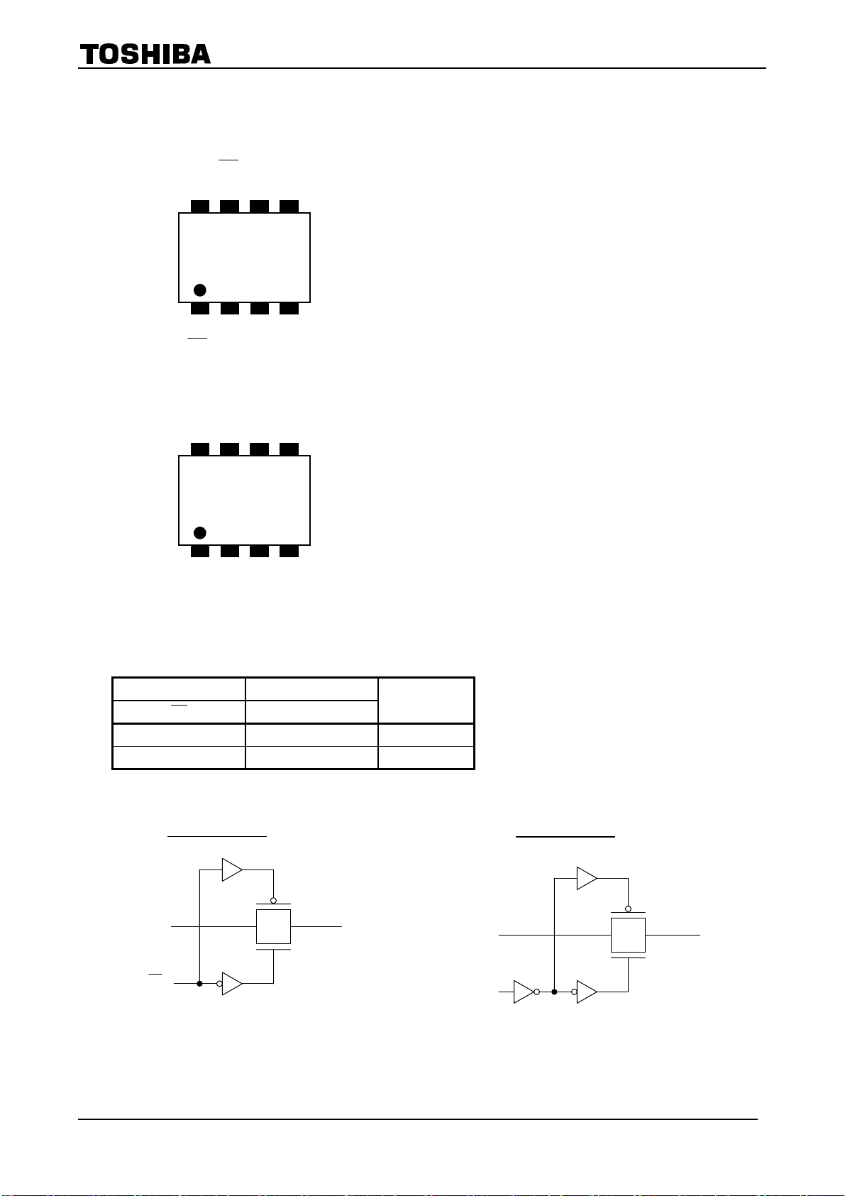
Pin Assignment (top view)
A
Truth Table
TC7WBL3306CFK
VCC
OE2
B2
8
7 6
W L C
336
5
1 2 3 4
OE1
1 B1
GND
TC7WBL3305CFK
VCC
OE2
B2
8
7 6
W L C
335
1 2 3 4
OE1
1 B1
5
GND
TC7WBL3306CFK,3305CFK
2
2
Inputs (3306C) Inputs (3305C)
OE
OE
L H A port = B port
H L Disconnect
System Diagram
TC7WBL3306C
An Bn
OEn
(n=1,2)
Function
TC7WBL3305C
An Bn
OEn
(n=1,2)
2
2009-07-01
Absolute Maximum Ratings (Note)
Characteristic Symbol Rating Unit
TC7WBL3306CFK,3305CFK
Power supply range V
Control pin input voltage (OE ,OE) V
Switch terminal I/O voltage
Clump diode current
Switch I/O current I
Power dissipation P
DC VCC/GND current ICC/I
Storage temperature T
VCC=0V or Switch=Off V
Switch=On V
CC
I
IK
stg
IN
S
S
S
D
GND
−0.5 to 4.6 V
−0.5 to 4.6 V
−0.5 to 4.6
−0.5 to VCC+0.5
−50
50 mA
200 mW
±100 mA
−65 to 150 °C
V
mA
Note: Exceeding any of the absolute maximum ratings, even briefly, lead to deterioration in IC performance or even
destruction
Using continuously under heavy loads (e.g. the application of high temperature/current/voltage and the
significant change in temperature, etc.) may cause this product to decrease in the reliability significantly even
if the operating conditions (i.e. operating temperature/current/voltage, etc.) are within the absolute maximum
ratings and the operating ranges.
Please design the appropriate reliability upon reviewing the Toshiba Semiconductor Reliability Handbook
(“Handling Precautions”/“Derating Concept and Methods”) and individual reliability data (i.e. reliability test
report and estimated failure rate, etc).
Operating Ranges (Note)
Note:
Characteristic Symbol Rating Unit
Power supply voltage V
Control pin input voltage (OE ,OE) V
Switch terminal I/O voltage
Operating temperature T
Input rise and fall time dt/dv 0 to 10 ns/V
VCC=0V or Switch=Off V
Switch=On V
CC
IN
S
S
opr
1.65 to 3.6 V
0 to VCC
0 to 3.6 V
0 to 3.6
−40 to 85 °C
V
The operating ranges must be maintained to ensure the normal operation of the device.
Unused inputs must be tied to either V
or GND.
CC
3
2009-07-01
 Loading...