现货库存、技术资料、百科信息、热点资讯,精彩尽在鼎好!
TOSHIBA CMOS Digital Integrated Circuit Silicon Monolithic
TC7WBL126AFK
Low-Voltage Dual Bus Switch
The TC7WBL126AFK provides two bits of low-voltage
high-speed bus switching. The low ON-resistance of the switch
allows connections to be made with minimal propagation delay
and while maintaining CMOS low power dissipation.
The device comprises dual 2-bit switches with separate bus
enable (OE) signals. When OE is high, the switch is on and port A
is connected to port B. When OE is low, the switch is off and a
high-impedance state exists between the two ports.
All inputs are equipped with protection circuits to guard
against static discharge.
Features
Weight: 0.01 g (typ.)
TC7WBL126AFK
• Operating voltage range: VCC = 2 to 3.6 V
• High speed: t
• Ultra-low ON-resistance: R
• ESD performance: Machine model ≥ ±200 V
Human body model ≥ ±2000 V
• Power-down protection provided on inputs (OE input only)
• Package: US8
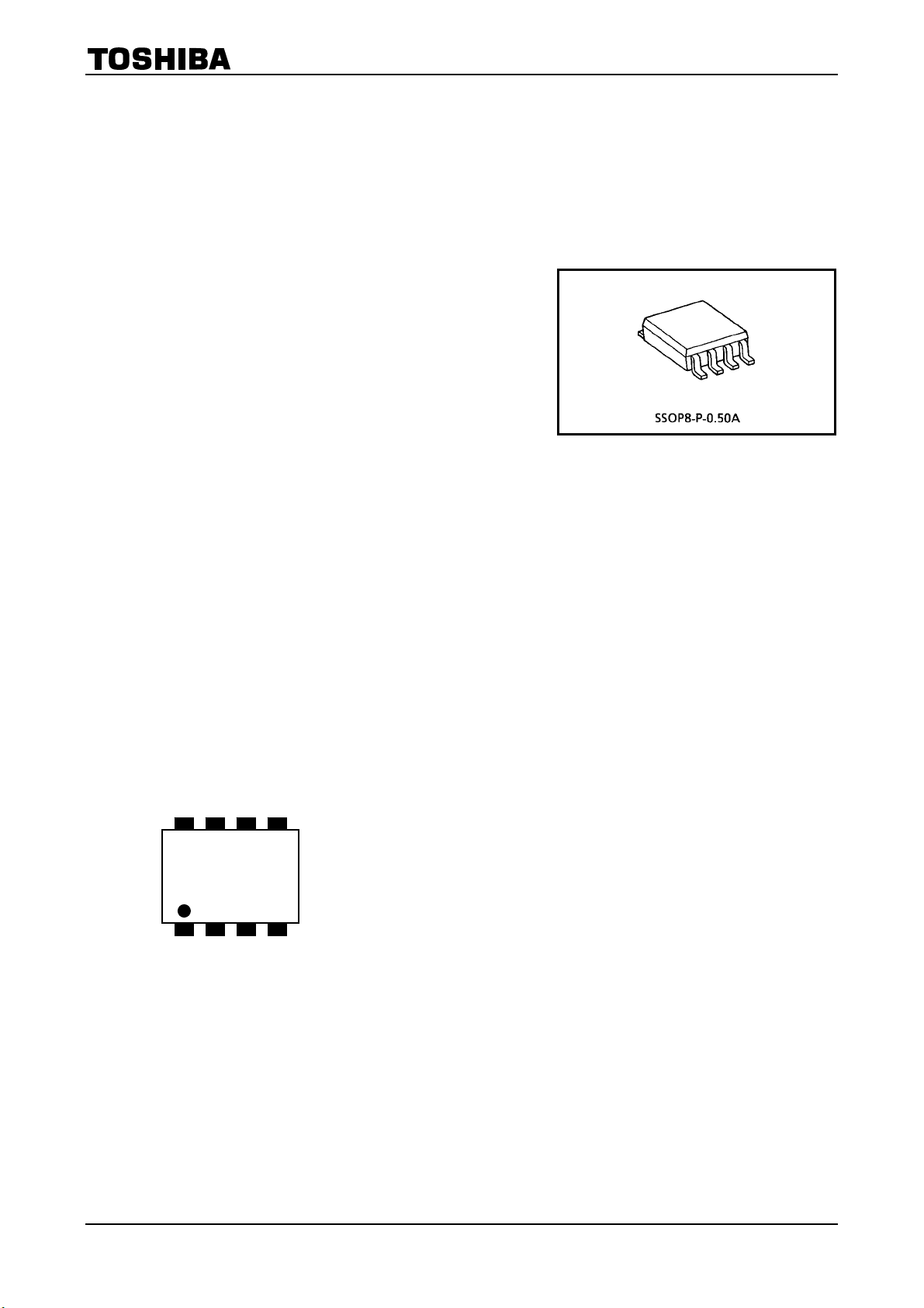
Pin Assignment
= 0.31 ns (max) @ 3 V
pd
(top view)
VCC
8
1 2 3 4
OE1
B1
OE2
7 6 5
W L A
1 2 6
A1 B2
GND
= 5 Ω (typ.) @ 3 V
ON
A2
1
2007-10-19

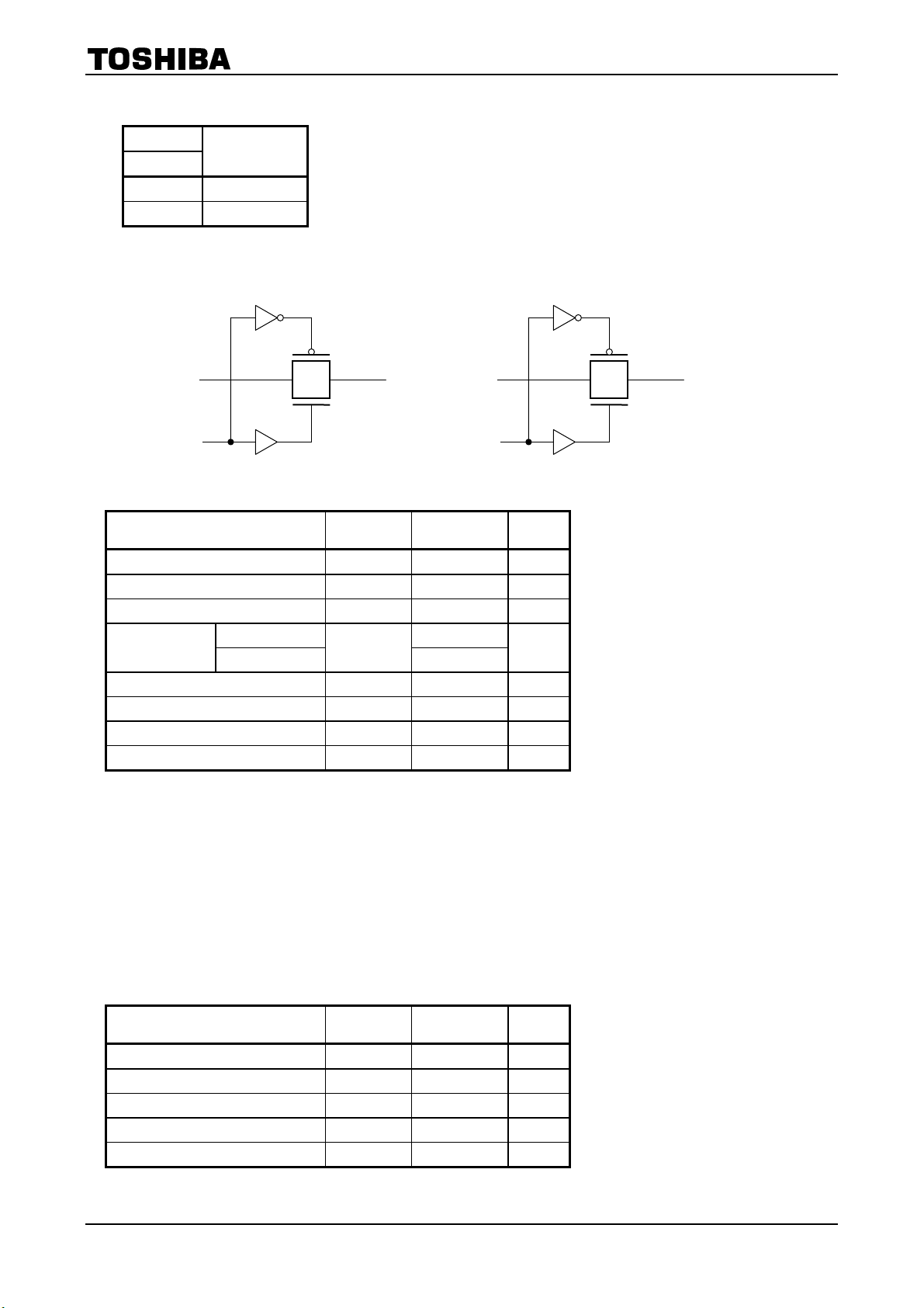
Truth Table
TC7WBL126AFK
Inputs
OE
H A port = B port
L Disconnect
Function
Logic Diagram
A1 B1
OE1
Absolute Maximum Ratings
Characteristic Symbol Rating Unit
Power supply range V
Control pin input voltage V
Switch terminal I/O voltage V
current
Switch I/O current I
Power dissipation P
DC VCC/GND current ICC/I
Storage temperature T
Control input pin −50 Clump diode
Switch terminal
(Note) (Ta = 25°C)
−0.5~4.6 V
−0.5~4.6 V
−0.5~Vcc+0.5 V
±50
128 mA
200 mW
±100 mA
−65~150 °C
I
CC
IK
stg
IN
S
S
D
GND
A2 B2
OE2
mA
Note: Exceeding any of the absolute maximum ratings, even briefly, lead to deterioration in IC performance or even
destruction.
Using continuously under heavy loads (e.g. the application of high temperature/current/voltage and the
significant change in temperature, etc.) may cause this product to decrease in the reliability significantly even
if the operating conditions (i.e. operating temperature/current/voltage, etc.) are within the absolute maximum
ratings and the operating ranges.
Please design the appropriate reliability upon reviewing the Toshiba Semiconductor Reliability Handbook
(“Handling Precautions”/“Derating Concept and Methods”) and individual reliability data (i.e. reliability test
report and estimated failure rate, etc).
Operating Ranges
Characteristic Symbol Rating Unit
Power supply voltage V
Control pin input voltage V
Switch I/O voltage V
Operating temperature T
Input rise and fall time dt/dv 0~10 ns/V
(Note)
CC
IN
opr
S
2.0~3.6 V
0~3.6 V
0~Vcc V
−40~85 °C
Note: The operating ranges must be maintained to ensure the normal operation of the device.
Unused inputs must be tied to either VCC or GND.
2
2007-10-19
 Loading...