

Toshiba TC7WBD126AFK Technical data
现货库存、技术资料、百科信息、热点资讯,精彩尽在鼎好!
TOSHIBA CMOS Dig ita l Integr ated Cir cu it Silicon Monolithic
TC7WBD126AFK
Dual Bus Switch with Level Shift
The TC7WBD126AFK is a low on-resistance, high-speed CMOS
2-bit bus switch. This bus switch allows the connections or
disconnections to be made with minimal propagation delay while
maintaining Low power dissipation which is the feature of
CMOS.
When output enable (OE) is at High level, the switch is on;
when at Low level, the switch is off.
The device is enable to realize the shift of signal level from 5 V
to 3.3 V.
All inputs are equipped with protector circuits to protect the
device from static discharge.
Features
Weight: 0.01 g (typ.)
TC7WBD126AFK
· Operating voltage: VCC = 4.5~5.5 V
· High speed operation: t
· Ultra-low on resistance: RON = 5 Ω (typ.)
· Electro-static discharge (ESD) performance: ±200 V or more (JEITA)
±2000 V or more (MIL)
· TTL level input (control input)
· Low Power Dissipation: Icc = 10 mA (max.)
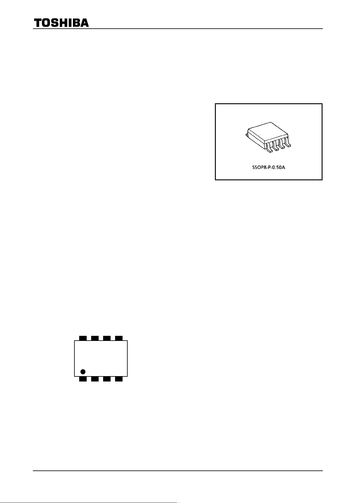
· Package: US8
Pin Assignment
VCC
8
= 0.32 ns (max)
pd
(top view)
B1 A2
OE2
7 6 5
W B A
1 2 6
1 2 3 4
OE1
A1 B2
GND
1
2002-10-18
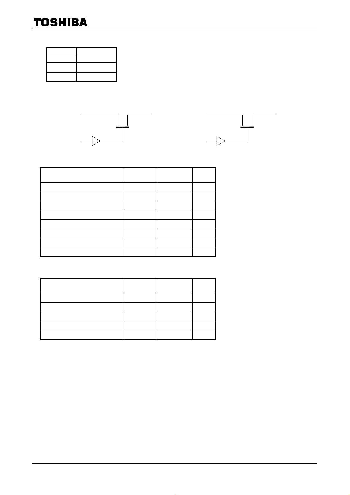
Truth Table
TC7WBD126AFK
Inputs
OE
L Disconnect
H A port = B port
Function
System Diagram
A1
OE1
B1 A2
Maximum Ratings
Characteristics Symbol Rating Unit
Power supply range V
DC input voltage V
DC switch voltage V
Input diode current I
Continuous channel current I
Power dissipation P
DC VCC/GND current ICC/I
Storage temperature T
CC
IN
S
IK
S
D
GND
stg
Recommended Operating Conditions
B2
OE2
-0.5~7.0 V
-0.5~7.0 V
-0.5~7.0 V
-50 mA
128 mA
200 mW
±100 mA
-65~150 °C
Characteristics Symbol Rating Unit
Supply voltage V
Input voltage V
Switch voltage V
Operating temperature T
Input rise and fall time dt/dv 0~10 ns/V
CC
IN
opr
S
4.5~5.5 V
0~5.5 V
0~5.5 V
-40~85 °C
2
2002-10-18
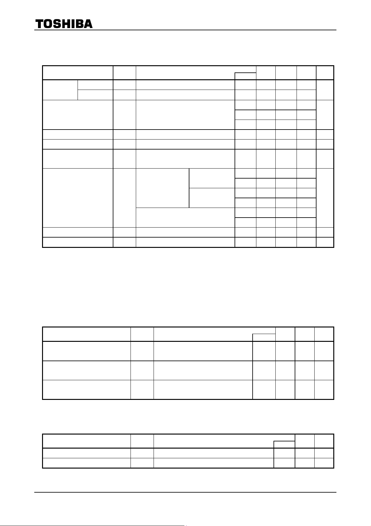
Electrical Characteristics
TC7WBD126AFK
DC Characteristics
Characteristics Symbol Test Condition
Input voltage
High-level output voltage
Input leakage current I
Power off leakage current I
Off-STATE leakage current
(switch off)
ON resistance
Quiescent supply current ICC VIN = VCC or GND,I
Increase in ICC per input DICC VIN = 3.4 V (one input) 5.5 ¾ ¾ 2.5 mA
“H” level
“L” level V
(Ta ==== ----40~85°C)
(Note 2)
(Note 3)
VIH ¾ 4.5~5.5 2.0 ¾ ¾
¾ 4.5~5.5 ¾ ¾ 0.8
IL
V
OH
IN
OFF
A, B = 0~5.5 V, OE = V
I
SZ
R
ON
(V)
Min
V
CC
IOH=-1mA
= V
V
IS
VIN = 0~5.5 V 4.5~5.5 ¾ ¾ ±1.0 mA
A, B, OE = 0~5.5 V 0 ¾ ¾ ±1.0 mA
VIS = 0 V
VIS = 2.3 V, IIS = 15 mA
CC
CC
IIS = 64 mA
I
= 30 mA
IS
= 0 5. 5 ¾ ¾ 10 mA
OUT
4.75 2.3 2.8 3.2
5.0 2.5 3.0 3.4
5.25 2.7 3.2 3.6
4.5~5.5 ¾ ¾ ±1.0 mA
4.5 ¾ 5 9
4.75 ¾ 5 8
4.5 ¾ 5 9
4.75 ¾ 5 8
4.5 ¾ 35 65
4.75 ¾ 35 50
Typ.
(Note 1)
Max Unit
V
V
W
Note 1: Typical values are at VCC = 5 V, Ta = 25°C.
Note 2: It recommends that this device uses Pull-up resistance when adding and using resistance for
an output terminal. Since it couses to drop a VOH voltage level when using Pull-down resistance
for an output terminal.
Note 3: Measured by the voltage drop between A and B pins at the indicated current through the switch. On
resistance is determined by the lower of the voltages on the two (A or B) pins.
AC Characteristics
Characteristics Symbol Test Condition
Propagation delay time
(bus to bus)
Output enable time
Output disable time
(Ta ==== ----40~85°C)
t
pLH
t
pHL
t
pZL
t
pZH
t
pLZ
t
pHZ
V
CC
Figure 1, Figure 2 (Note 4) 4.5 ¾ 0.32 ns
Figure 1, Figure 3 4.5 ¾ 4.5 ns
Figure 1, Figure 3 4.5 ¾ 5.5 ns
Min Max Unit
(V)
Note 4: The propagation delay time is calculated by the RC (on-resistance and load capacitance) time constant.
Capacitive Characteristics
(Ta ==== 25°C)
Characteristics Symbol Test Condition
Control pin input capacitance CIN (Note 5) 5.0 3 pF
Switch terminal capacitance C
OE = VCC (Note 5) 5.0 10 pF
I/O
(V)
Typ. Unit
V
CC
Note 5: This parameter is guaranteed by design.
3
2002-10-18
 Loading...