

Toshiba TC7WBD125FK Technical data
现货库存、技术资料、百科信息、热点资讯,精彩尽在鼎好!
TOSHIBA CMO S Digital I ntegrat ed Circ uit Silicon Monolithic
TC7WBD125FK
Dual Bus Switch with Level Shift
The TC7WBD125FK is a low on-resistance, high-speed CMOS
2-bit bus switch. This bus switch allows the connections or
disconnections to be made with minimal propagation delay while
maintaining Low power dissipation which is the feature of
CMOS.
When output enable (OE) is at low level, the switch is on; when
at high level, the switch is off.
The internal diode which adds to power supply line is enable to
realize the shift of signal level from 5 V to 3.3 V. (Note 1)
All inputs are equipped with protector circuits to protect the
device from static discharge.
Features
Weight: 0.01 g (typ.)
TC7WBD125FK
• Operating voltage: V
• High speed operation: t
• Ultra-low on resistance: RON = 5 Ω (typ.)
• Electro-static discharge (ESD) performance: ±200 V or more (JEITA)
±2000 V or more (MIL)
• TTL level input (control input)
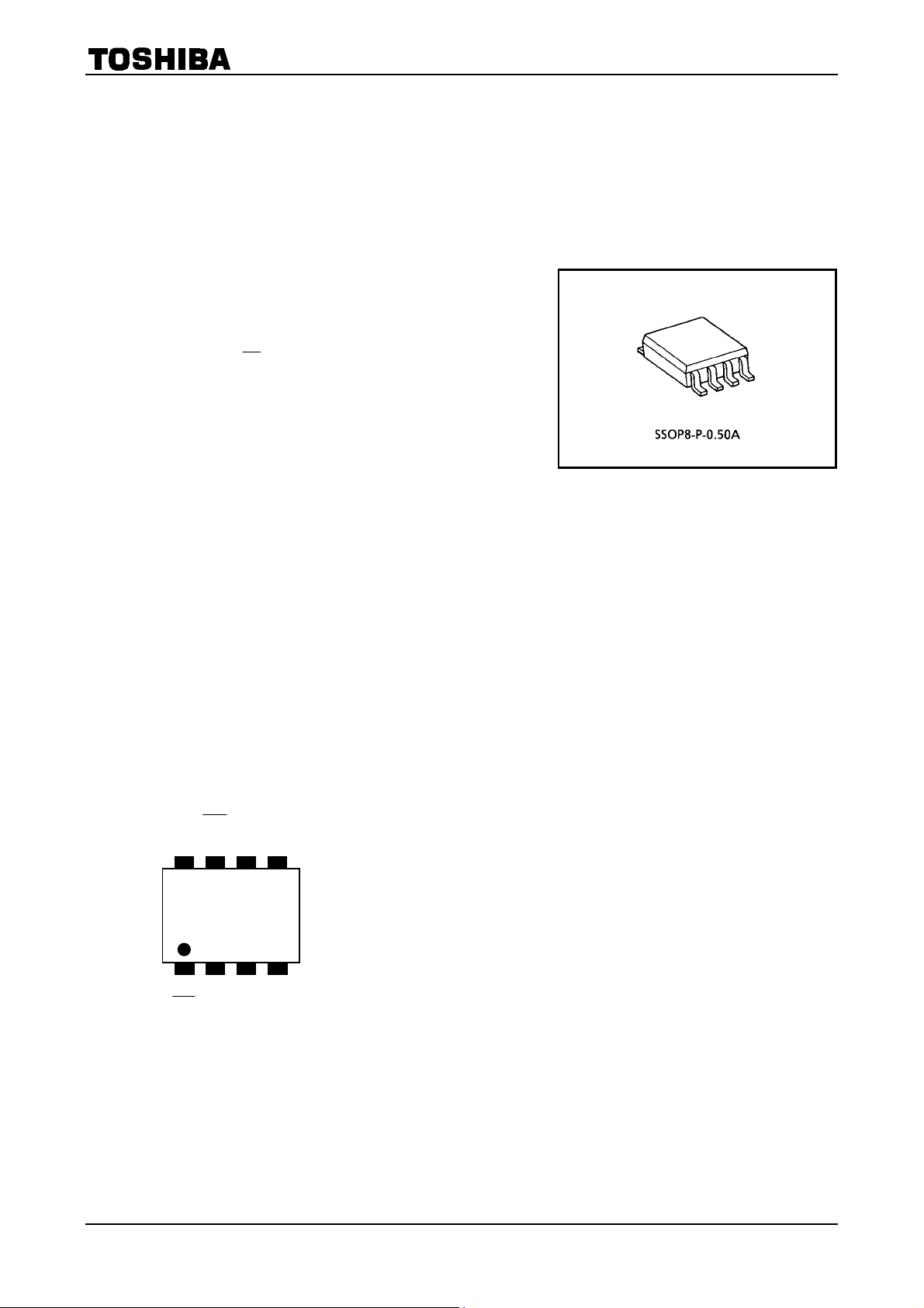
• Package: US8
Note 1: In case that over-shoot noise is detected, this device should be used with clamp diode to prevent the next
stage device from over-stress.
Pin Assignment
VCC
8
7 6
W B D
1 2 5
= 4.5~5.5 V
CC
= 0.25 ns (max)
pd
(top view)
B1 A2
2OE
5
1 2 3 4
A1 B2
OE1
GND
1
2001-12-04
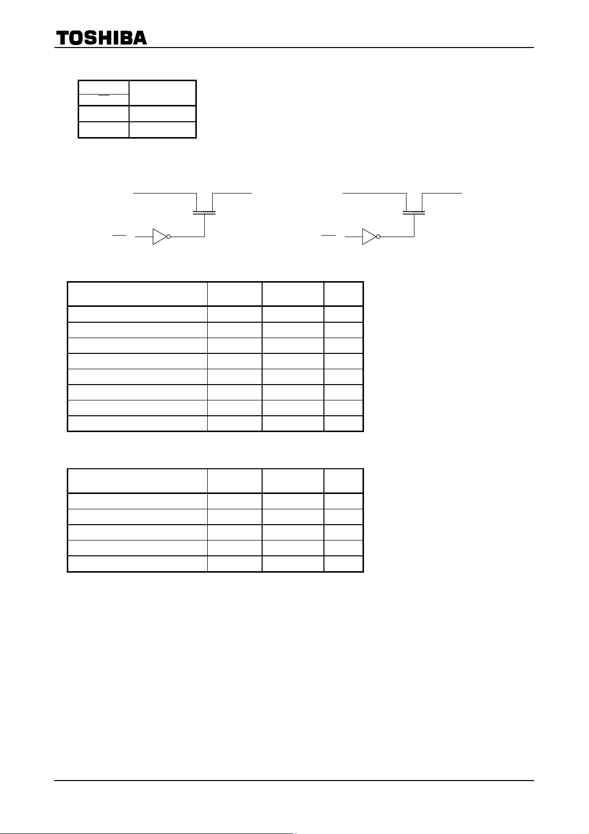
Truth Table
TC7WBD125FK
Inputs
OE
L A port = B port
H Disconnect
Function
System Diagram
A1
OE1
B1
A2
2OE
Maximum Ratings
Characteristics Symbol Rating Unit
Power supply voltage V
Control pin input voltage V
Switch terminal I/O voltage V
Clump diode current IIK −50 mA
Switch I/O current I
Power dissipation P
DC VCC/GND current ICC/I
Storage temperature T
CC
IN
S
S
D
GND
stg
−0.5~7.0 V
−0.5~7.0 V
−0.5~7.0 V
128 mA
200 mW
±100 mA
−65~150 °C
Recommended Operating Conditions
B2
Characteristics Symbol Rating Unit
Power supply voltage V
Control pin input voltage V
Switch I/O voltage V
Operating temperature T
Control pin input rise/fall time dt/dv 0~10 ns/V
CC
IN
opr
S
4.5~5.5 V
0~5.5 V
0~5.5 V
−40~85 °C
2
2001-12-04
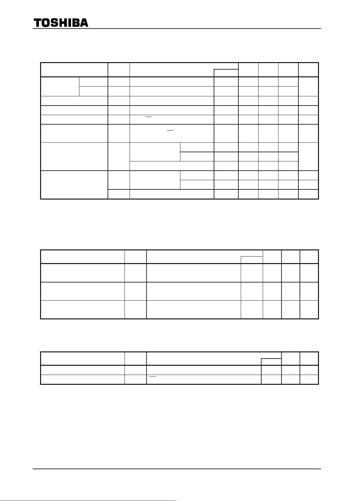
Electrical Characteristics
TC7WBD125FK
DC Characteristics
Characteristics Symbol Test Condition
Control pin input
voltage
High-level output voltage VOH Figure 4
Input leakage current I
Power off leakage current I
Off-state leakage current
(switch off)
ON resistance (Note 3) R
Quiescent supply current
“H” level
“L” level V
(Ta ==== −−−−40~85°C)
VIH 4.5~5.5 2.0
4.5~5.5 0.8
IL
IN
A, B, OE = 0~5.5 V 0 ±1.0 µA
OFF
A, B = 0~5.5 V, OE = V
I
SZ
ON
ICC
∆I
VIN = 3.4 V (one input) 5.5 2.5 mA
CC
V
CC
VIN = 0~5.5 V 4.5~5.5 ±1.0 µA
CC
VIS = 0 V
VIS = 2.4 V, IIS = 15 mA 4.5 35 50
= VCC or GND
V
IN
I
= 0
OUT
IIS = 64 mA 4.5 5 7
= 30 mA 4.5 5 7
I
IS
switch ON 5.5 1.5 mA
switch OFF 5.5 10 µA
4.5~5.5 ±1.0 µA
(V)
Min
Typ.
(Note 2)
Max Unit
Note 2: The typical values are at VCC = 5 V, Ta = 25°C.
Note 3: Apply the specified current to the switch, then measure the voltages on pins A and B. The on-resistance is
the lower of the two.
AC Characteristics
(Ta ==== −−−−40~85°C)
V
Ω
Characteristics Symbol Test Condition
Propagation delay time
(bus to bus)
Output enable time
Output disable time
t
pLH
Figure 1, Figure 2 (Note 4) 4.5 0.25 ns
t
pHL
t
pZL
Figure 1, Figure 3 4.5 4.5 ns
t
pZH
t
pLZ
Figure 1, Figure 3 4.5 5.0 ns
t
pHZ
V
CC
Min Max Unit
(V)
Note 4: The propagation delay time is calculated by the RC (on-resistance and load capacitance) time constant.
Capacitive Characteristics
Characteristics Symbol Test Condition
Control pin input capacitance CIN (Note 5) 5.0 3 pF
Switch terminal capacitance C
(Ta ==== 25°C)
OE
I/O
V
CC
= VCC (Note 5) 5.0 10 pF
Typ. Unit
(V)
Note 5: This parameter is guaranteed by design.
3
2001-12-04
 Loading...