

现货库存、技术资料、百科信息、热点资讯,精彩尽在鼎好!
TOSHIBA CMO S Digital I ntegrat ed Circ uit Silicon Monolithic
TC7WB383FK
2-Bit Bus Exchange Switch
The TC7WB383FK is a low on-resistance, high-speed CMOS
2-bit bus exchange switch. This bus switch allows the connections
or disconnections to be made with minimal propagation delay
while maintaining Low power dissipation which is the feature of
CMOS.
When output enable (OE) is at high level, the switches are off.
When at low level, the switches are on, and by the logic of EX
terminal, It can choose whether 2 bits data are transferred to the
corresponding terminal as it is, or the data are transferred to a
terminal with exchanging data line. Therefore it may be used as
2 to 1 multiplexer switch.
Since the switch channels consist of N type MOSFET, the high
level output voltage is provided about 1 V lower than V
All inputs are equipped with protection circuits to protect the
device from static discharge.
CC
level.
Features
Weight: 0.01 g (typ.)
TC7WB383FK
• Operating voltage: V
• High speed operation: t
• Ultra-low on resistance: RON = 5 Ω (typ.)
• Electro-static discharge (ESD) performance: ±200 V or more (JEITA)
±2000 V or more (MIL)
• TTL level input (control input)
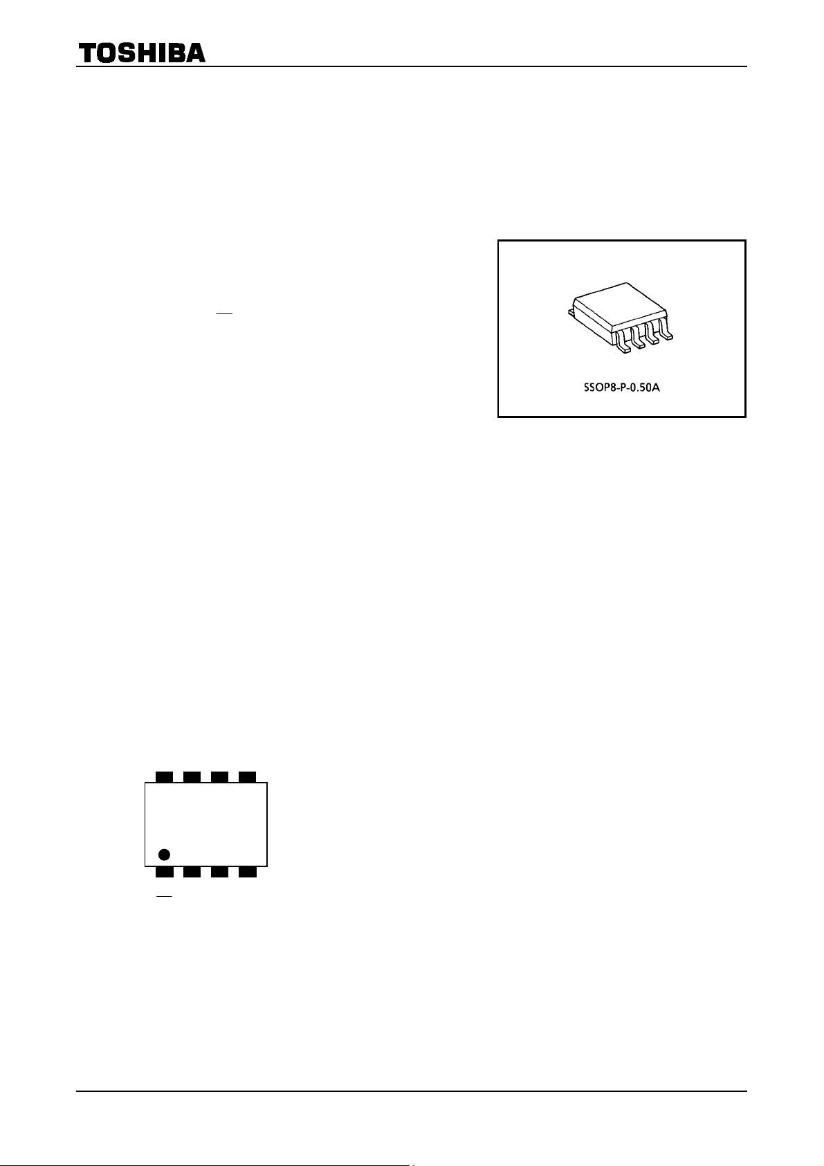
• Package: US8
Pin Assignment
VCC 8 C1 D1 EX
7 6
3 8 3
1 2 3 4
A1 B1
OE
= 4.5~5.5 V
CC
pd
(top view)
W B
GND
= 0.25 ns (max)
5
1
2001-09-17
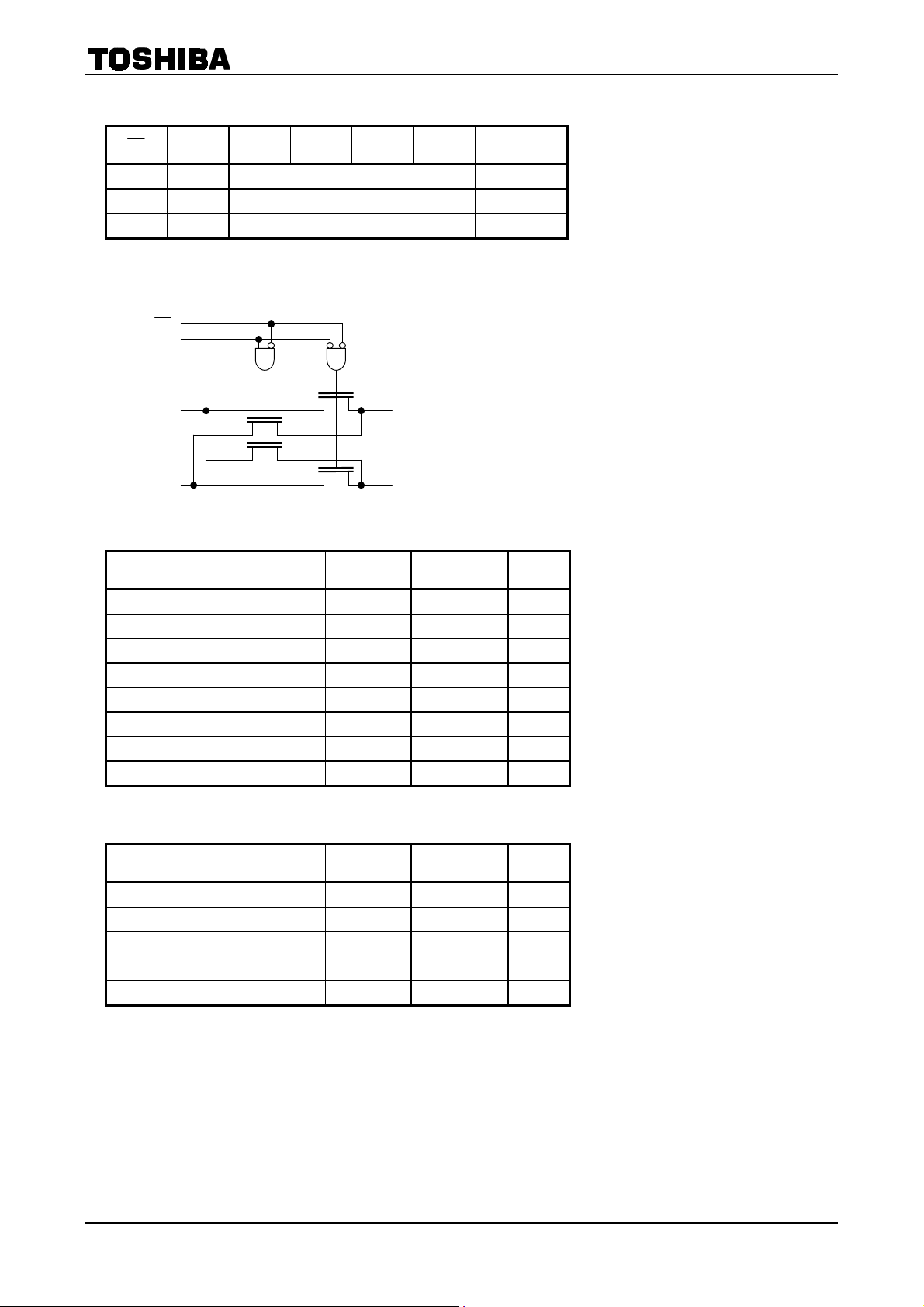
Truth Table
EX A1 B1 C1 D1 Function
OE
H X Hi-Z Disconnect
L L A1 = C1, B1 = D1 Connect
L H A1 = D1, B1 = C1 Exchange
System Diagram
OE
EX
TC7WB383FK
A1
B1 D1
C1
Maximum Ratings
Characteristics Symbol Rating Unit
Power supply voltage V
Control pin input voltage V
Switch terminal I/O voltage V
Clump diode current IIK −50 mA
Switch I/O current I
Power dissipation P
DC VCC/GND current ICC/I
Storage temperature T
CC
IN
S
S
D
GND
stg
−0.5~7.0 V
−0.5~7.0 V
−0.5~7.0 V
128 mA
200 mW
±100 mA
−65~150 °C
Recommended Operating Conditions
Characteristics Symbol Rating Unit
Power supply voltage V
Control pin input voltage V
Switch I/O voltage V
Operating temperature T
Control pin input rise/fall time dt/dv 0~10 ns/V
CC
IN
opr
S
4.5~5.5 V
0~5.5 V
0~5.5 V
−40~85 °C
2
2001-09-17
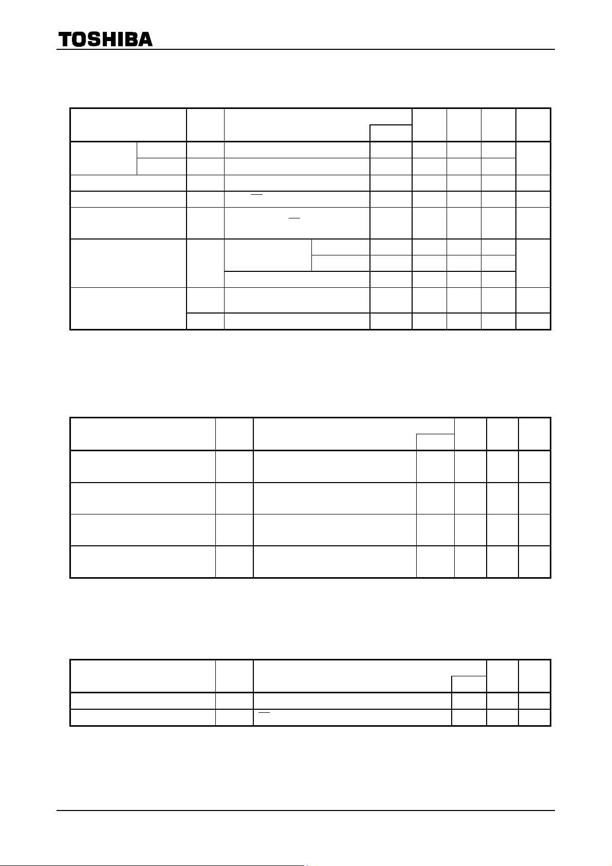
Electrical Characteristics
TC7WB383FK
DC Characteristics
Characteristics Symbol Test Condition
Control pin input
voltage
Input leakage current I
Power off leakage current I
Off-state leakage current
(switch off)
ON resistance (Not e 2) R
Quiescent supply current
“H” level
“L” level V
(Ta ==== −−−−40~85°C)
VIH 4.5~5.5 2.0
4.5~5.5 0.8
IL
IN
A, B, OE = 0~5.5 V 0 ±1.0 µA
OFF
A, B = 0~5.5 V, OE = V
I
SZ
ON
ICC
VIN = 3.4 V (one input) 5.5 2.5 mA
∆I
CC
V
CC
VIN = 0~5.5 V 4.5~5.5 ±1.0 µA
CC
VIS = 0 V
VIS = 2.4 V, IIS = 15 mA 4.5 10 15
= VCC or GND
V
IN
I
= 0
OUT
IIS = 64 mA 4.5 5 7
= 30 mA 4.5 5 7
I
IS
4.5~5.5 ±1.0 µA
5.5 10 mA
Min
(V)
Typ.
(Note 1)
Note 1: The typical values are at VCC = 5 V, Ta = 25°C.
Note 2: Measured by the voltage drop between A and B pins at the indicated current through the switch. On
resistance is determined by the lower of the voltages on two (A or B) pins.
AC Characteristics
(Ta ==== −−−−40~85°C)
Max Unit
V
Ω
Characteristics Symbol Test Condition
Propagation delay time
(bus to bus)
Propagation delay time
(EX to bus)
Output enable time
Output disable time
t
pLH
Figure 1, Figure 2 (Note 3) 4.5 0.25 ns
t
pHL
t
pLH
Figure 1, Figure 3 4.5 4.5 ns
t
pHL
t
pZL
Figure 1, Figure 4 4.5 4.5 ns
t
pZH
t
pLZ
Figure 1, Figure 4 4.5 5.5 ns
t
pHZ
V
CC
Min Max Unit
(V)
Note 3: This parameter is guaranteed by design but is not tested. The bus switch contributes no propagation delay
other than the RC delay of the typical on resistance of the switch and the 50 pF load capacitance, when
driven by an ideal voltage the source (zero output impedance).
Capacitive Characteristics
Characteristics Symbol Test Condition
Control pin input capacitance CIN (Note 4) 5.0 3 pF
Switch terminal capacitance C
(Ta ==== 25°C)
OE
I/O
V
CC
= VCC (Note 4) 5.0 17 pF
Typ. Unit
(V)
Note 4: This item is guaranteed by design.
3
2001-09-17

AC Test Circuit
p
V
Out
AC Waveform
ut
Switch
L
C
Input
(A, B, C, D)
R
L
R
Measure
L
C
R
Open
7.0 V
GND
= 50 pF
L
= 500 Ω
L
tr 2.5 ns
Figure 1
tf 2.5 ns
90%
1.5
Parameter Switch
, t
pHL
, t
pZL
, t
Open
pZH
Open
7.0 V
3.0 V
GND
10%
t
pLH
t
t
pHZ
pLZ
TC7WB383FK
V
Output
(A, B, C, D)
t
pLH
Figure 2 t
pLH
, t
1.5 V
t
pHL
pHL
OH
V
OL
Exchange
(EX)
Output
(A, B, C, D)
Output
(A, B, C, D)
tr 2.5 ns
t
pLH
t
pHL
90%
1.5 V
tf 2.5 ns
10%
t
pHL
1.5 V
1.5 V
t
pLH
3.0 V
GND
V
OH
V
OL
V
OH
V
OL
Figure 3 t
pLH
, t
pHL
4
2001-09-17

TC7WB383FK
t
2.5 ns tr 2.5 ns
f
Output Enable
(
)
OE
Output (A, B, C, D)
Low to Off to Low
Output (A, B, C, D)
High to Off to High
t
t
Outputs
enabled
pLZ
pHZ
90%
1.5 V
V
+
OL
0.3 V
VOH − 0.3 V
Outputs
disabled
10%
t
t
pZL
pZH
1.5 V
1.5 V
Outputs
enabled
3.0 V
GND
3.5 V
VOL
V
OH
GND
Figure 4 t
pLZ
, t
pHZ
, t
pZL
, t
pZH
5
2001-09-17

Package Dimensions
TC7WB383FK
Weight: 0.01 g (typ.)
6
2001-09-17

TC7WB383FK
A
RESTRICTIONS ON PRODUCT USE
• TOSHIBA is continually working to improve the quality and reliability of its products. Nevertheless, semiconductor
devices in general can malfunction or fail due to their inherent electrical sensitivity and vulnerability to physical
stress. It is the responsibility of the buyer, when utilizing TOSHIBA products, to comply with the standards of
safety in making a safe design for the entire system, and to avoid situations in which a malfunction or failure of
such TOSHIBA products could cause loss of human life, bodily injury or damage to property.
In developing your designs, please ensure that TOSHIBA products are used within specified operating ranges as
set forth in the most recent TOSHIBA products specifications. Also, please keep in mind the precautions and
conditions set forth in the “Handling Guide for Semiconductor Devices,” or “TOSHIBA Semiconductor Reliability
Handbook” etc..
• The TOSHIBA products listed in this document are intended for usage in general electronics applications
(computer, personal equipment, office equipment, measuring equipment, industrial robotics, domestic appliances,
etc.). These TOSHIBA products are neither intended nor warranted for usage in equipment that requires
extraordinarily high quality and/or reliability or a malfunction or failure of which may cause loss of human life or
bodily injury (“Unintended Usage”). Unintended Usage include atomic energy control instruments, airplane or
spaceship instruments, transportation instruments, traffic signal instruments, combustion control instruments,
medical instruments, all types of safety devices, etc.. Unintended Usage of TOSHIBA products listed in this
document shall be made at the customer’s own risk.
• The products described in this document are subject to the foreign exchange and foreign trade laws.
• The information contained herein is presented only as a guide for the applications of our products. No
responsibility is assumed by TOSHIBA CORPORATION for any infringements of intellectual property or other
rights of the third parties which may result from its use. No license is granted by implication or otherwise under
any intellectual property or other rights of TOSHIBA CORPORATION or others.
000707EB
• The information contained herein is subject to change without notice.
7
2001-09-17
 Loading...