

Toshiba TC7WB126FK Technical data
现货库存、技术资料、百科信息、热点资讯,精彩尽在鼎好!
TOSHIBA CMOS Digital Integrated Circuit Silicon Monolithic
TC7WB126FK
Dual Bus Switch
The TC7WB126FK is a low on-resistance, high-speed CMOS
dual-bit bus switch. This bus switch allows the connections or
disconnections to be made with minimal propagation delay while
maintaining Low power dissipation which is the feature of
CMOS.
When output enable (OE) is at High level, the switch is on;
when at Low level, the switch is off.
All inputs are equipped with protector circuits to protect the
device from static discharge.
Features
· Operating voltage: V
· High speed operation: tpd = 0.25 ns (max)
· Ultra-low on resistance: RON = 5 Ω (typ.)
· Electro-static discharge (ESD) performance: ±200 V or more (JEITA)
±2000 V or more (MIL)
· TTL level input (control input)
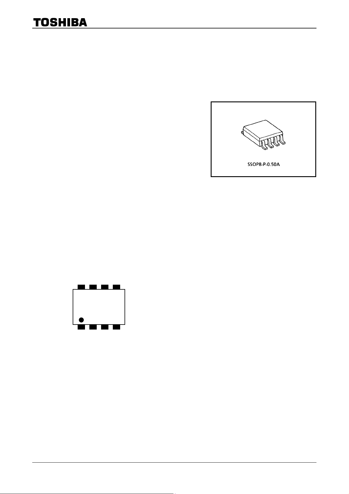
· Package: US8
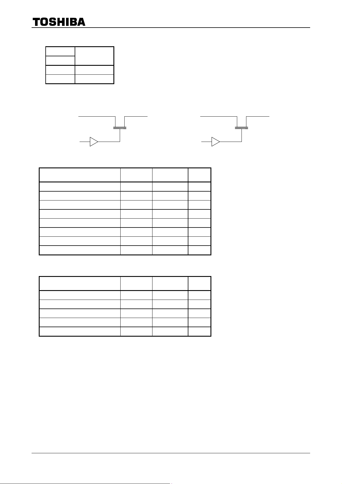
Pin Assignment
= 4.5~5.5 V
CC
(top view)
Weight: 0.01 g (typ.)
TC7WB126FK
VCC
8
1 2 3 4
OE1
B1
OE2
7 6 5
W B
1 2 6
A1 B2
A2
GND
1
2001-09-17
Truth Table
TC7WB126FK
Inputs
OE
L Disconnect
H A port = B port
Function
System Diagram
A1
OE1
B1 A2
Maximum Ratings
Characteristics Symbol Rating Unit
Power supply range V
DC input voltage V
DC switch voltage V
Input diode current I
Continuous channel current I
Power dissipation P
DC VCC/GND current ICC/I
Storage temperature T
CC
IN
S
IK
S
D
GND
stg
Recommended Operating Conditions
B2
OE2
-0.5~7.0 V
-0.5~7.0 V
-0.5~7.0 V
-50 mA
128 mA
200 mW
±100 mA
-65~150 °C
Characteristics Symbol Rating Unit
Supply voltage V
Input voltage V
Switch voltage V
Operating temperature T
Input rise and fall time dt/dv 0~10 ns/V
CC
IN
opr
S
4.5~5.5 V
0~5.5 V
0~5.5 V
-40~85 °C
2
2001-09-17
 Loading...