

TOSHIBA TC7SHU04FE Technical data

现货库存、技术资料、百科信息、热点资讯,精彩尽在鼎好!
TOSHIBA CMOS Digital Integrated Circuit Silicon Monolithic
TC7SHU04FE
INVERTER (Un-Buffer)
Features
• Super high speed operation : tPD = 3.5 ns (typ.)
@V
• Low power dissipation : I
CC
@ Ta = 25°C
• High noise immunity : V
NIH
= 10% V
• 5.5V tolerant input.
•
Wide operation
voltage range : V
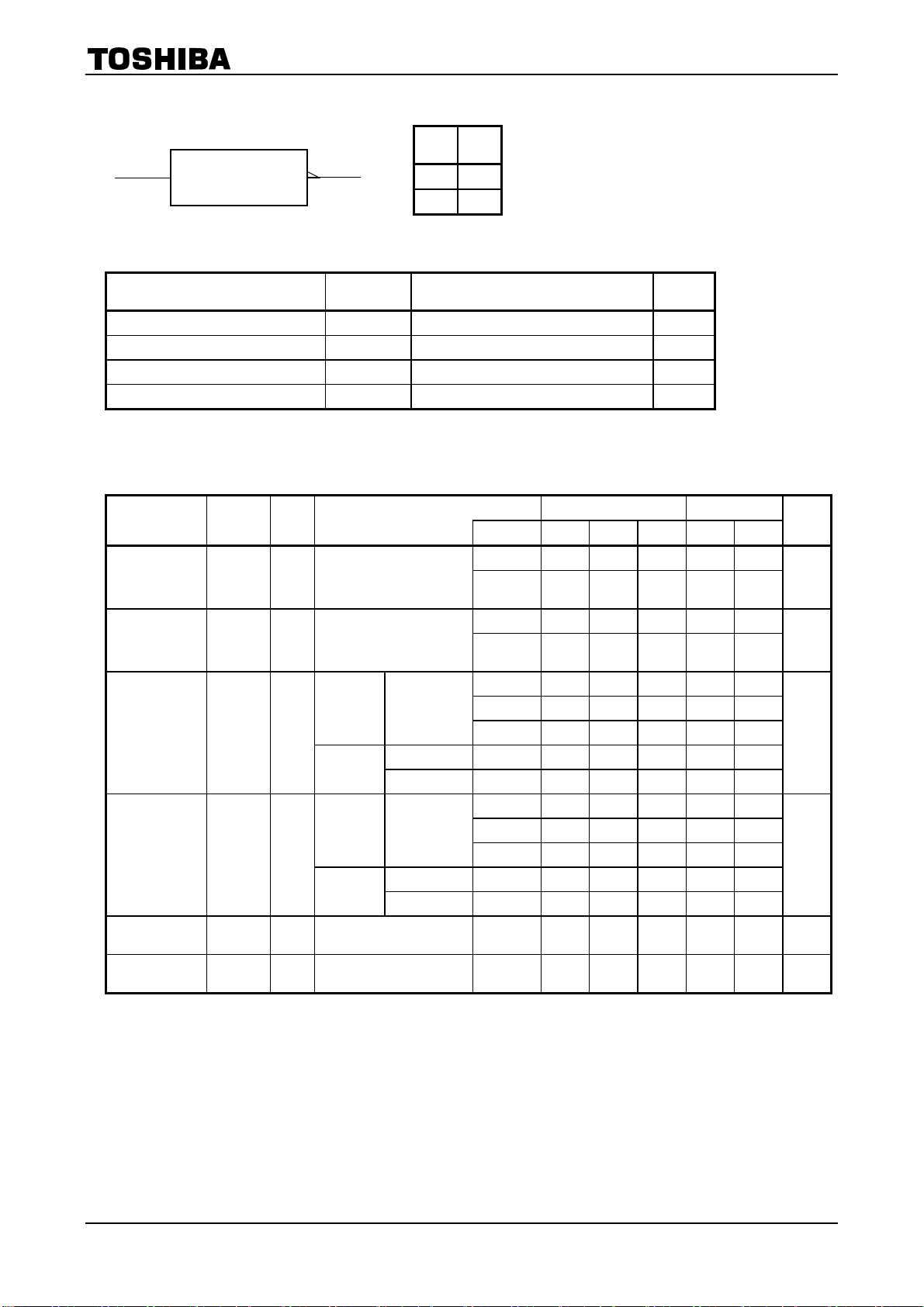
Marking Pin Assignment
= 5 V
CC
= 2 μA (Max.)
= V
NIH
(Min.)
CC
(opr) = 2~5.5 V
CC
Weight: 0.003 g (typ.)
TC7SHU04FE
(top view)
H 6
Type name
NC
IN A
1
2
Absolute Maximum Ratings
Characteristics Symbol Rating Unit
Supply voltage range V
DC input voltage V
DC output voltage V
Input diode current I
Output diode current I
DC output current I
DC VCC/ground current ICC ±50 mA
Power dissipation PD 150 mW
Storage temperature T
(Ta = 25°C)
CC
IN
OUT
IK
OK
OUT
stg
GND
3
−0.5~7 V
−0.5~7 V
−0.5~VCC + 0.5 V
−20 mA
±20 mA
±25 mA
−65~150 °C
5
4
V
CC
OUT Y
Note: Using continuously under heavy loads (e.g. the application of high temperature/current/voltage and the
significant change in temperature, etc.) may cause this product to decrease in the reliability significantly even
if the operating conditions (i.e. operating temperature/current/voltage, etc.) are within the absolute maximum
ratings and the operating ranges.
Please design the appropriate reliability upon reviewing the Toshiba Semiconductor Reliability Handbook
(“Handling Precautions”/“Derating Concept and Methods”) and individual reliability data (i.e. reliability test
report and estimated failure rate, etc).
1
2007-11-01
Logic Diagram Truth Table
A Y
TC7SHU04FE
IN A
1
OUT Y
L H
H L
Operating Ranges
Characteristics Symbol Rating Unit
Supply voltage VCC 2~5.5 V
Input voltage VIN 0~5.5
Output voltage V
Operating temperature T
0~ VCC V
OUT
opr
−40~85 °C
V
Electrical Characteristics
DC Characteristics
Characteristics Symbol
High-level input
voltage
Low-level input
voltage
High-level
output voltage
Low-level output
voltage
Input leakage
current
Quiescent
supply current
V
V
V
V
I
I
CC
IH
IL
OH
OL
IN
Test
Circuit
⎯
⎯
⎯
⎯
⎯ VIN = 5.5 V or GND 0~5.5 ⎯ ⎯ ±0.1 ⎯ ±1.0 μA
⎯ VIN = VCC or GND 5.5 ⎯ ⎯ 2.0 ⎯ 20.0 μA
Test Condition
⎯
⎯
VIN = VIL IOH = −50 μA
V
=GND
IN
VIN = VIH IOL = 50 μA
V
IN =VCC
IOH = −4 mA 3.0 2.58
= −8 mA 4.5 3.94
I
OH
IOL = 4 mA 3.0 ⎯ ⎯ 0.36 ⎯ 0.44
I
= 8 mA 4.5 ⎯ ⎯ 0.36 ⎯ 0.44
OL
Ta = 25°C Ta = −40~85°C
(V)
V
CC
2.0 1.7 ⎯ ⎯ 1.7 ⎯
3.0~5.5
2.0 ⎯ ⎯ 0.3 ⎯ 0.3
3.0~5.5 ⎯ ⎯
2.0 1.8 2.0 ⎯ 1.8 ⎯
3.0 2.7 3.0 ⎯ 2.7 ⎯
4.5 4.0 4.5 ⎯ 4.0 ⎯
2.0 ⎯ 0 0.2 ⎯ 0.2
3.0 ⎯ 0 0.3 ⎯ 0.3
4.5 ⎯ 0 0.5 ⎯ 0.5
Min Typ. Max Min Max
V
CC
× 0.8
⎯ ⎯
V
× 0.2
⎯
⎯
VCC
× 0.8
CC
⎯ 2.48 ⎯
⎯ 3.80 ⎯
⎯
VCC
× 0.2
⎯
Unit
V
V
V
V
2
2007-11-01
 Loading...