

Toshiba TC7SH08F, TC7SH08FU Schematic [ru]
TOSHIBA CMOS Digital Integrated Circuit Silicon Monolithic
TC7SH08F, TC7SH08FU
2-Input AND Gate
Features
• High speed operation : tpd = 4.3ns (typ.) at VCC = 5V, 15pF
• Low power dissipation : I
• High noise immunity : V
= 2 μA (max) at Ta = 25°C
CC
= V
NIH
= 28% V
NIL
CC
(min)
• 5.5-V tolerant inputs
• Wide operating voltage range : V
= 2 to 5.5 V
CC
Marking
TC7SH08F
TC7SH08FU
TC7SH08F/FU
(SMV)
Product name
H 2
Absolute Maximum Ratings
Characteristics Symbol Rating Unit
Supply voltage V
DC input voltage V
DC output voltage V
Input diode current I
Output diode current I
DC output current I
DC VCC/ground current ICC ± 50 mA
Power dissipation PD 200 mW
Storage temperature T
Lead temperature (10 s) T
(Ta = 25°C)
CC
IN
OUT
IK
OK
OUT
stg
L
− 0.5 to 7 V
− 0.5 to 7 V
− 0.5 to VCC + 0.5 V
− 20 mA
± 20 (Note1) mA
± 25 mA
− 65 to 150 °C
260 °C
Weight
SSOP5-P-0.95 : 0.016 g (typ.)
SSOP5-P-0.65A : 0.006 g (typ.)
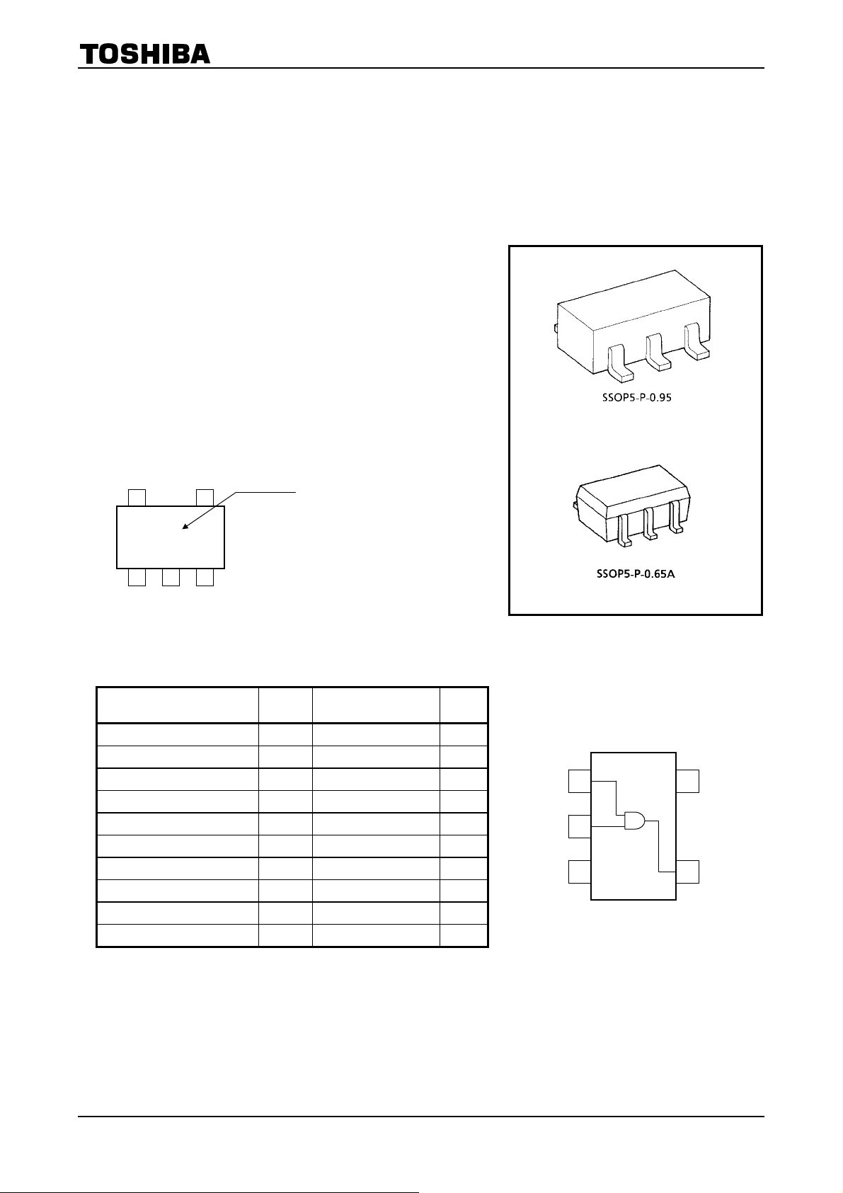
Pin Assignment
(top view)
IN B 1
IN A 2
GND 3
5 V
4 OUT Y
(USV)
CC
Note: Using continuously under heavy loads (e.g. the application of high temperature/current/voltage and the
significant change in temperature, etc.) may cause this product to decrease in the reliability significantly even
if the operating conditions (i.e. operating temperature/current/voltage, etc.) are within the absolute maximum
ratings and the operating ranges.
Please design the appropriate reliability upon reviewing the Toshiba Semiconductor Reliability Handbook
(“Handling Precautions”/“Derating Concept and Methods”) and individual reliability data (i.e. reliability test
report and estimated failure rate, etc).
Note1: V
< GND, V
OUT
OUT
> VCC
1
2009-09-09
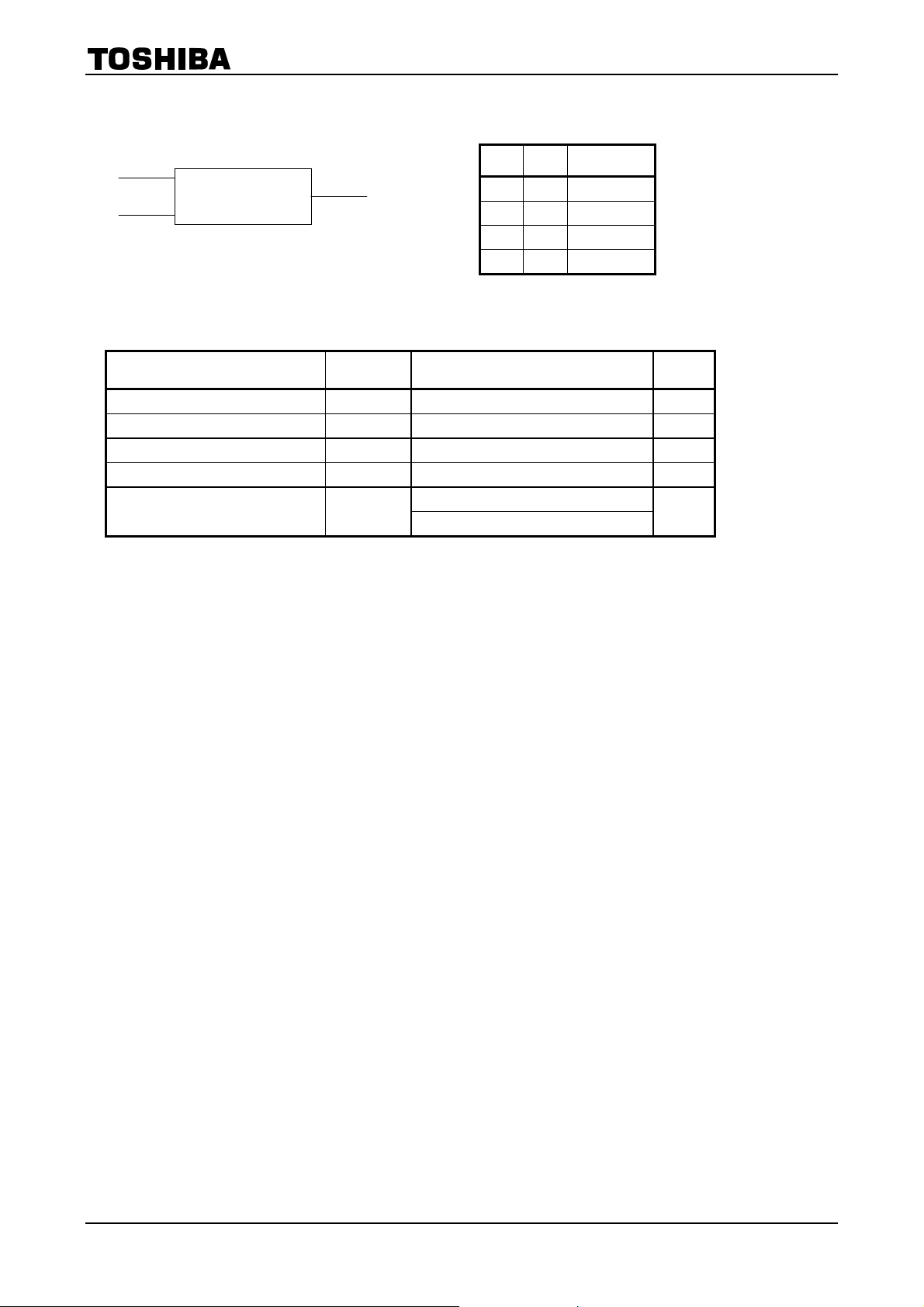
IEC Logic Symbol Truth Table
IN A
IN B
A B
OUT Y
&
L L L
L H L
H L L
H H H
Y
Operating Ranges
Characteristics Symbol Rating Unit
Supply voltage VCC 2.0 to 5.5 V
Input voltage VIN 0 to 5.5
Output voltage V
Operating temperature T
Input rise and fall time dt/dv
0 to VCC V
OUT
opr
0 to 100 (VCC = 3.3±0.3V)
0 to 20 (VCC = 5.0±0.5V)
−40 to 85 °C
TC7SH08F/FU
V
ns/V
2
2009-09-09
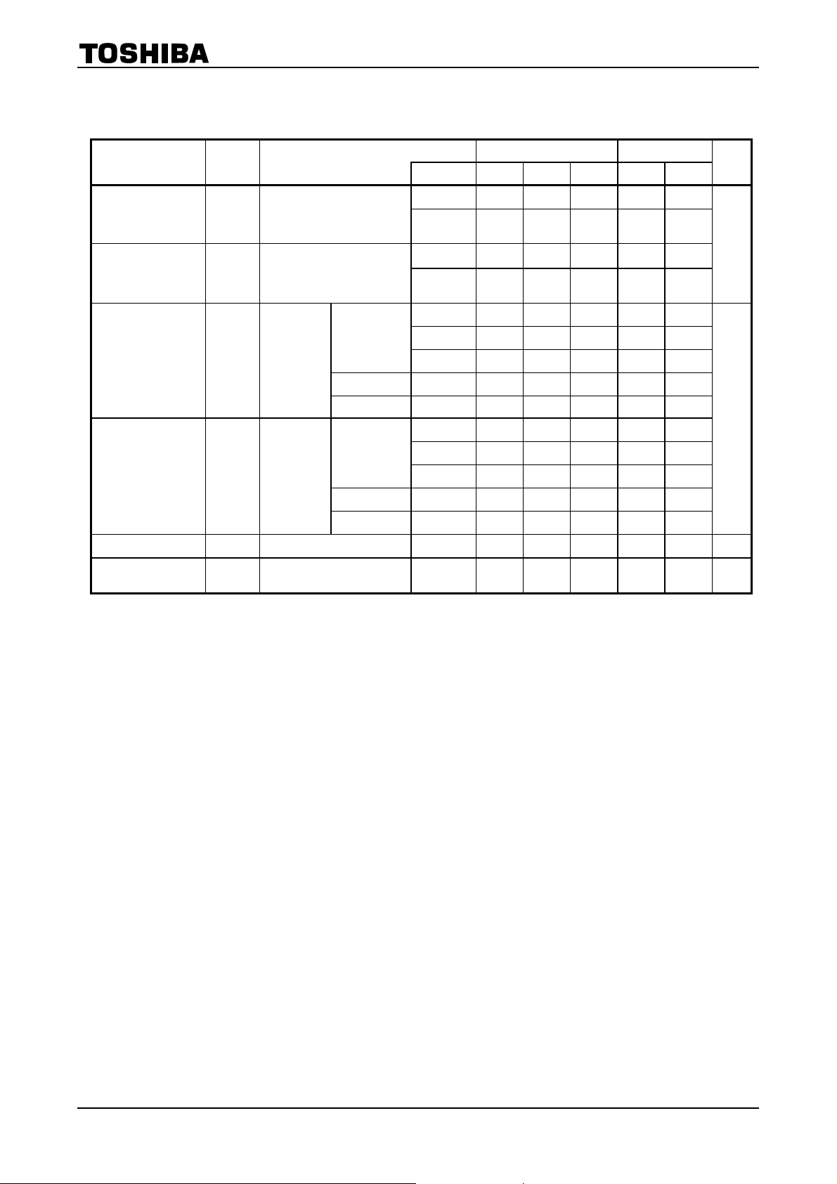
Electrical Characteristics
DC Characteristics
TC7SH08F/FU
Characteristics Symbol Test Condition
High-level
input voltage
Low-level
input voltage
High-level
output voltage
Low-level
output voltage
Input leakage current I
Quiescent supply
current
V
IH
V
IL
VIN = VIH
V
OH
V
OL
IN
I
CC VIN
V
= V
IN
IH or
VIL
VIN = 5.5 V or GND
= VCC or GND
⎯
⎯
IOH = −50 μA
IOH = −4 mA
IOH = −8 mA
IOL = 50 μA
IOL = 4mA
= 8 mA
I
OL
Ta = 25°C Ta = −40 to 85°C
(V)
V
CC
2.0 1.5
3.0 to 5.5
2.0
3.0 to 5.5
2.0 1.9 2.0
3.0 2.9 3.0
4.5 4.4 4.5
3.0 2.58
4.5 3.94
2.0
3.0
4.5
3.0
4.5
0 to 5.5
5.5
Min Typ. Max Min Max
1.5
VCC
× 0.7
⎯
⎯
1.9
2.9
4.4
2.48
3.80
⎯
⎯
⎯
⎯
⎯
⎯
⎯
V
CC
× 0.7
⎯
⎯
⎯
⎯
⎯
⎯ ⎯
⎯ ⎯
⎯ ⎯
⎯ ⎯
⎯
⎯
⎯
⎯
⎯ ⎯
⎯ ⎯
0 0.10
0 0.10
0 0.10
⎯
⎯
0.5
V
CC
× 0.3
⎯
⎯
⎯
0.36
0.36
±0.1
2.0
⎯
⎯
0.5
V
CC
× 0.3
⎯
⎯
⎯
⎯
⎯
0.10
0.10
0.10
0.44
0.44
±1.0
20.0
Unit
V
V
μA
μA
3
2009-09-09
 Loading...