

TC74VHC595F/FN/FT/FK
TOSHIBA CMOS Digital Integrated Circuit Silicon Monolithic
TC74VHC595F,TC74VHC595FN,TC74VHC595FT,TC74VHC595FK
8-Bit Shift Register/Latch (3-state)
The TC74VHC595 is an advanced high speed 8-BIT SHIFT
REGISTER/LATCH fabricated with silicon gate C
It achieves the high speed operation similar to equivalent Bipolar
Schottky TTL while maintaining the CMOS low power dissipation.
The TC74VHC595 contains an 8-bit static shift register which
feeds an 8-bit storage register.
Shift operation is accomplished on the positive going transition of
the SCK input. The output register is loaded with the contents of
the shift register on the positive going transition of the RCK input.
Since RCK and SCK signal are independent, parallel outputs can be
held stable during the shift operation. And, since the parallel
outputs are 3-state, it can be directly connected to 8-bit bus. This
register can be used in serial-to-parallel conversion, data receivers,
etc.
An input protection circuit ensures that 0 to 5.5 V can be applied
to the input pins without regard to the supply voltage. This device
can be used to interface 5 V to 3 V systems and two supply systems
such as battery back up. This circuit prevents device destruction
due to mismatched supply and input voltages.
2
MOS technology.
Features
Note: xxxFN (JEDEC SOP) is not available in
Japan.
TC74VHC595F
TC74VHC595FN
TC74VHC595FT
• High speed: f
• Low power dissipation: I
• High noise immunity: V
• Power down protection is provided on all inputs.
• Balanced propagation delays: t
• Wide operating voltage range: V
• Low noise: V
• Pin and function compatible with 74ALS595
= 185 MHz (typ.) at VCC = 5 V
max
= 4 μA (max) at Ta = 25°C
CC
= 1.0 V (max)
OLP
NIH
= V
= 28% VCC (min)
NIL
∼
t
−
pLH
(opr) = 2 V to 5.5 V
CC
pHL
TC74VHC595FK
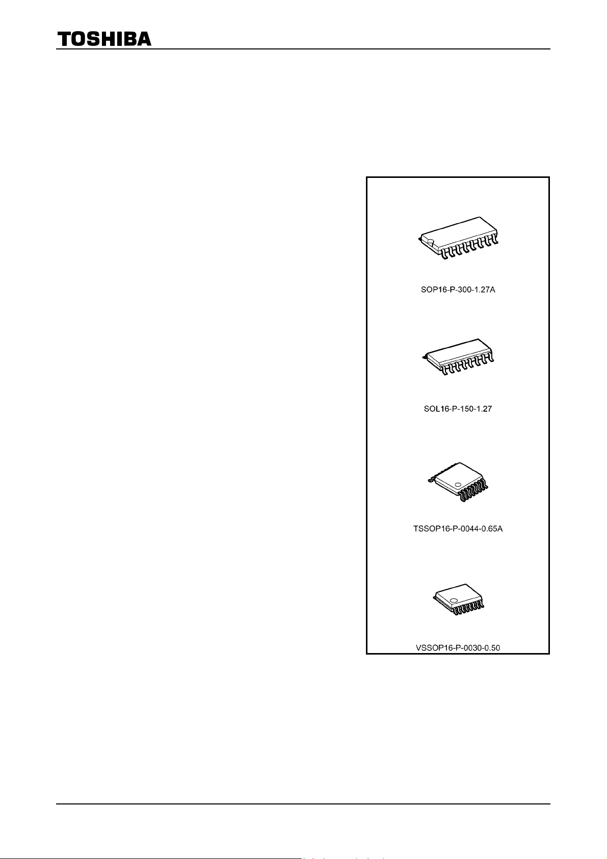
Weight
SOP16-P-300-1.27A : 0.18 g (typ.)
SOL16-P-150-1.27 : 0.13 g (typ.)
TSSOP16-P-0044-0.65A : 0.06 g (typ.)
VSSOP16-P-0030-0.50 : 0.02 g (typ.)
1
2007-10-01
TC74VHC595F/FN/FT/FK
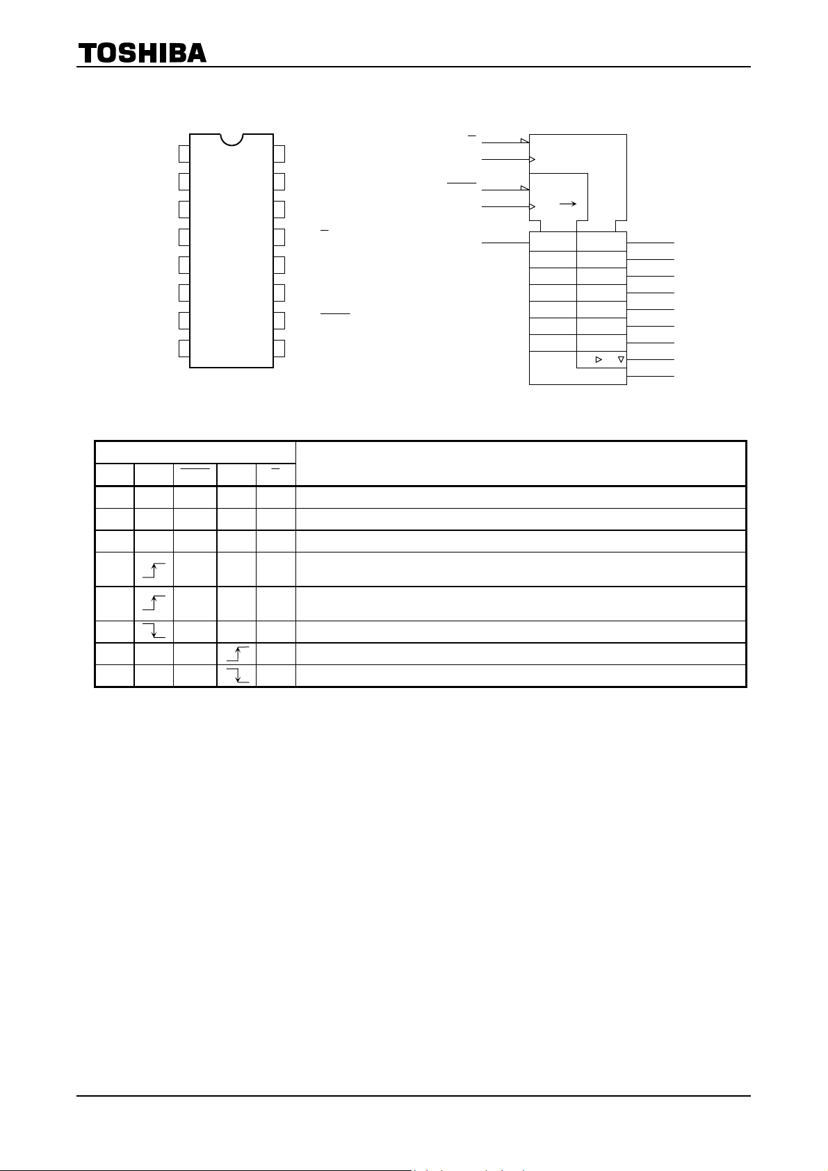
Pin Assignment IEC Logic Symbol
(13)
QB
QC
QD
16
15
14
VCC
QA
SI
1
2
3
G
SCLR
SCK
(12)
(10)
(11)
EN3
C
R
C/1
RCK
2
SRG8
QE
QF
QG
QH
GND
4
5
6
7
8
(top view)
13
12
10
9
G
RCK
SCK 11
SCLR
QH’
Truth Table
Inputs
SI SCK SCLR RCK G
X X X X H QA thru QH outputs disable
X X X X L QA thru QH outputs enable
X X L X X Shift register is cleared.
L
H H X X
X H X X State of S.R. is not changed.
X X X X S.R. data is stored into storage register.
X X X X Storage register stage is not changed.
H X X
First stage of S.R. becomes “L”. Other stages store the data of previous stage,
respectively.
First stage of S.R. becomes “H”. Other stages store the data of previous stage,
respectively.
SI
(14)
Function
1D
2D 3
2D 3
(15)
(1)
(2)
(3)
(4)
(5)
(6)
(7)
(9)
QA
QB
QC
QD
QE
QF
QG
QH
QH’
X: Don’t care
2
2007-10-01
Timing Chart
SCK
SI
RCK
SCLR
G
QA
QB
QC
QD
QE
TC74VHC595F/FN/FT/FK
QF
QG
QH
QH’
System Diagram
10
SCLR
14
SI
11
SCK
12
RCK
RR RRRRRR
D D
Q D
SCK
SCK
RCK
SCK
QD D D DD D D D DQ Q Q Q Q Q Q
RCK
SCK
RCK
D
D D D D DQ QQQQQQ
SCK
RCK
SCK
RCK
SCK
RCK
SCK
RCK
QH’
9
RCK
13
G
15
QA
1
QB
2
QC
3
QD
4
QE
5
QF
6
QG
7
QH
3
2007-10-01
TC74VHC595F/FN/FT/FK
Absolute Maximum Ratings (Note)
Characteristics Symbol Rating Unit
Supply voltage range VCC −0.5 to 7.0 V
DC input voltage VIN −0.5 to 7.0 V
DC output voltage V
Input diode current IIK −20 mA
Output diode current IOK ±20 mA
DC output current I
DC VCC/ground current ICC ±75 mA
Power dissipation PD 180 mW
Storage temperature T
Note: Exceeding any of the absolute maximum ratings, even briefly, lead to deterioration in IC performance or
even destruction.
Using continuously under heavy loads (e.g. the application of high temperature/current/voltage and the
significant change in temperature, etc.) may cause this product to decrease in the reliability significantly
even if the operating conditions (i.e. operating temperature/current/voltage, etc.) are within the absolute
maximum ratings and the operating ranges.
Please design the appropriate reliability upon reviewing the Toshiba Semiconductor Reliability Handbook
(“Handling Precautions”/“Derating Concept and Methods”) and individual reliability data (i.e. reliability test
report and estimated failure rate, etc).
Operating Ranges (Note)
−0.5 to VCC + 0.5 V
OUT
±25 mA
OUT
−65 to 150 °C
stg
Characteristics Symbol Rating Unit
Supply voltage V
Input voltage V
Output voltage V
Operating temperature T
Input rise and fall time dt/dv
CC
IN
OUT
opr
0 to 100 (V
2.0 to 5.5 V
0 to 5.5
0 to V
CC
−40 to 85 °C
= 3.3 ± 0.3 V)
CC
0 to 20 (V
= 5 ± 0.5 V)
CC
Note: The operating ranges must be maintained to ensure the normal operation of the device.
Unused inputs must be tied to either VCC or GND.
V
V
ns/V
4
2007-10-01

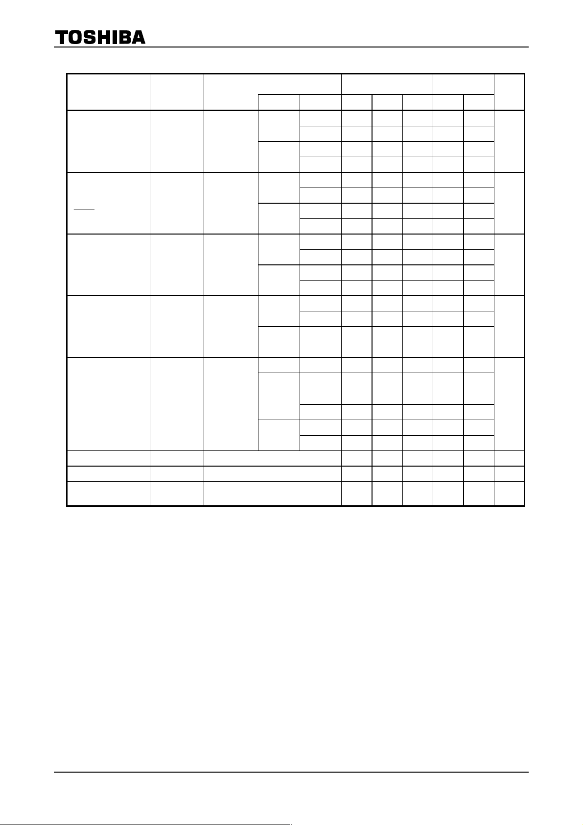
Electrical Characteristics
DC Characteristics
Characteristics Symbol
High-level input
voltage
Low-level input
voltage
High-level output
voltage
Low-level output
voltage
V
IH
V
IL
V
OH
V
OL
V
= V
V
V
= V
V
IN
or
IH
IL
IN
or
IH
IL
Test Condition
―
―
IOH = −50 μA
= −4 mA
I
OH
IOH = −8 mA
IOL = 50 μA
= 4 mA
I
OL
IOL = 8 mA
TC74VHC595F/FN/FT/FK
Ta = 25°C
V
CC
Min Typ. Max Min Max
(V)
2.0
1.50
3.0
V
CC
to
0.7
5.5
2.0
―
3.0
to
―
5.5
2.0
1.9
3.0
2.9
4.5
4.4
3.0
2.58
4.5
3.94― ―
2.0
―
3.0
―
4.5
―
3.0
4.5― ―
×
―
―
―
―
2.0
3.0
4.5
0.50
V
CC
0.3
―
―
―
―
―
― ― 2.48
0.0
0.0
0.0
0.1
0.1
0.1
― ― 0.36
0.36 ― ―
×
Ta =
−40 to 85°C
1.50
V
×
CC
0.7
―
V
―
1.9
2.9
4.4
3.80 ― ―
―
―
―
―
―
0.50
CC
0.3
―
―
―
0.1
0.1
0.1
0.44
0.44
×
Unit
V
V
V
V
3-state output
off-state current
Input leakage
current
Quiescent supply
current
I
I
I
CC
OZ
IN
V
OUT
VIN = 5.5 V or GND
= VCC or GND
5.5 ― ― ±0.25 ― ±2.50 μA
0 to
― ― ±0.1 ― ±1.0 μA
5.5
= VIH or VIL
V
IN
VIN = VCC or GND 5.5 ― ― 4.0 ― 40.0 μA
5
2007-10-01

TC74VHC595F/FN/FT/FK
Timing Requirements
Characteristics Symbol
Minimum pulse width
(SCK, RCK)
Minimum pulse width
(
SCLR )
Minimum set-up time
(SI-SCK)
Minimum set-up time
(SCK-RCK)
Minimum set-up time
(
-RCK)
SCLR
Minimum hold time
(SI-SCK)
Minimum hold time
(SCK-RCK)
Minimum hold time
(
SCLR -RCK)
Minimum removal time
(
)
SCLR
(input: tr = tf = 3 ns)
t
w (H)
t
w (L)
t
w (L)
t
―
s
t
―
s
―
t
s
t
―
h
t
―
h
―
t
h
―
t
rem
Test Condition
―
―
Ta =
5.0
5.0
5.0
5.0
3.5
3.0
8.0
5.0
8.0
5.0
1.5
2.0
0
0
0
0
3.0
2.5
−40 to
85°C
5.0
5.0
5.0
5.0
3.5
3.0
8.5
5.0
9.0
5.0
1.5
2.0
0
0
0
0
3.0
2.5
Unit
ns
ns
ns
ns
ns
ns
ns
ns
ns
Ta = 25°C
V
(V) Typ. Limit Limit
CC
3.3 ± 0.3
5.0 ± 0.5― ―
3.3 ± 0.3
5.0 ± 0.5― ―
3.3 ± 0.3
5.0 ± 0.5― ―
3.3 ± 0.3
5.0 ± 0.5― ―
3.3 ± 0.3
5.0 ± 0.5― ―
3.3 ± 0.3
5.0 ± 0.5― ―
3.3 ± 0.3
5.0 ± 0.5― ―
3.3 ± 0.3
5.0 ± 0.5― ―
3.3 ± 0.3
5.0 ± 0.5― ―
6
2007-10-01
TC74VHC595F/FN/FT/FK
AC Characteristics
Characteristics Symbol
Propagation delay
time
(SCK-QH’)
Propagation delay
time
(
-QH’)
SCLR
Propagation delay
time
(RCK-Q
Output enable time
Output disable time
Maximum clock
frequency
Input capacitance CIN ― ― 4 10 ― 10 pF
Output capacitance C
Power dissipation
capacitance
)
n
(input: tr = tf = 3 ns)
t
pLH
t
pHL
t
pHL
t
pLH
t
pHL
t
pZL
t
pZH
t
pLZ
t
pHZ
f
―
max
― ― 6 ― ― ― pF
OUT
C
(Note) ― 87 ― ― ― pF
PD
―
―
―
RL = 1 kΩ
RL = 1 kΩ
Test Condition Ta = 25°C
V
(V) CL (pF) Min Typ. Max Min Max
CC
3.3 ± 0.3
5.0 ± 0.5
3.3 ± 0.3
5.0 ± 0.5
3.3 ± 0.3
5.0 ± 0.5
3.3 ± 0.3
5.0 ± 0.5
3.3 ± 0.3 50 ― 12.1 15.7 1.0 16.2
5.0 ± 0.5 50 ― 7.6 10.3 1.0 11.0
3.3 ± 0.3
5.0 ± 0.5
15 ― 8.8 13.0 1.0 15.0
50 ― 11.3 16.5 1.0 18.5
15 ― 6.2 8.2 1.0 9.4
50 ― 7.7 10.2 1.0 11.4
15 ― 8.4 12.8 1.0 13.7
50 ― 10.9 16.3 1.0 17.2
15 ― 5.9 8.0 1.0 9.1
50 ― 7.4 10.0 1.0 11.1
15 ― 7.7 11.9 1.0 13.5
50 ― 10.2 15.4 1.0 17.0
15 ― 5.4 7.4 1.0 8.5
50 ― 6.9 9.4 1.0 10.5
15 ― 7.5 11.5 1.0 13.5
50 ― 9.0 15.0 1.0 17.0
15 ― 4.8 8.6 1.0 10.0
50 ― 8.3 10.6 1.0 12.0
15 80 150 ― 70 ―
50 55 130 ― 50 ―
15 135 185 ― 115 ―
50 95 155 ― 85 ―
Ta =
−40 to 85°C
Unit
ns
ns
ns
ns
ns
MHz
Note: CPD is defined as the value of the internal equivalent capacitance which is calculated from the operating
current consumption without load.
Average operating current can be obtained by the equation:
I
= CPD·VCC·fIN + ICC
CC (opr)
7
2007-10-01

TC74VHC595F/FN/FT/FK
Noise Characteristics (input: tr = tf = 3 ns)
Characteristics Symbol
Quiet output maximum dynamic VOL V
Quiet output minimum dynamic VOL V
Minimum high level dynamic input
voltage
Maximum low level dynamic input
voltage
V
V
OLP
OLV
IHD
ILD
Input Equivalent Circuit
INPUT
Test Condition
CL = 50 pF 5.0 0.8 1.0 V
CL = 50 pF 5.0 −0.8 −1.0 V
CL = 50 pF 5.0 ― 3.5 V
CL = 50 pF 5.0 ― 1.5 V
Ta = 25°C
VCC (V) Typ. Limit
Unit
8
2007-10-01

Package Dimensions
TC74VHC595F/FN/FT/FK
Weight: 0.18 g (typ.)
9
2007-10-01

Package Dimensions (Note)
TC74VHC595F/FN/FT/FK
Note: This package is not available in Japan.
Weight: 0.13 g (typ.)
10
2007-10-01

Package Dimensions
TC74VHC595F/FN/FT/FK
Weight: 0.06 g (typ.)
11
2007-10-01

Package Dimensions
TC74VHC595F/FN/FT/FK
Weight: 0.02 g (typ.)
12
2007-10-01

TC74VHC595F/FN/FT/FK
RESTRICTIONS ON PRODUCT USE
• Toshiba Corporation, and its subsidiaries and affiliates (collectively “TOSHIBA”), reserve the right to make changes to the information
in this document, and related hardware, software and systems (collectively “Product”) without notice.
• This document and any information herein may not be reproduced without prior written permission from TOSHIBA. Even with
TOSHIBA’s written permission, reproduction is permissible only if reproduction is without alteration/omission.
• Though TOSHIBA works continually to improve Product’s quality and reliability, Product can malfunction or fail. Customers are
responsible for complying with safety standards and for providing adequate designs and safeguards for their hardware, software and
systems which minimize risk and avoid situations in which a malfunction or failure of Product could cause loss of human life, bodily
injury or damage to property, including data loss or corruption. Before creating and producing designs and using, customers must
also refer to and comply with (a) the latest versions of all relevant TOSHIBA information, including without limitation, this document,
the specifications, the data sheets and application notes for Product and the precautions and conditions set forth in the “TOSHIBA
Semiconductor Reliability Handbook” and (b) the instructions for the application that Product will be used with or for. Customers are
solely responsible for all aspects of their own product design or applications, including but not limited to (a) determining the
appropriateness of the use of this Product in such design or applications; (b) evaluating and determining the applicability of any
information contained in this document, or in charts, diagrams, programs, algorithms, sample application circuits, or any other
referenced documents; and (c) validating all operating parameters for such designs and applications.
LIABILITY FOR CUSTOMERS’ PRODUCT DESIGN OR APPLICATIONS.
• Product is intended for use in general electronics applications (e.g., computers, personal equipment, office equipment, measuring
equipment, industrial robots and home electronics appliances) or for specific applications as expressly stated in this document.
Product is neither intended nor warranted for use in equipment or systems that require extraordinarily high levels of quality and/or
reliability and/or a malfunction or failure of which may cause loss of human life, bodily injury, serious property damage or serious
public impact (“Unintended Use”). Unintended Use includes, without limitation, equipment used in nuclear facilities, equipment used
in the aerospace industry, medical equipment, equipment used for automobiles, trains, ships and other transportation, traffic signaling
equipment, equipment used to control combustions or explosions, safety devices, elevators and escalators, devices related to electric
power, and equipment used in finance-related fields. Do not use Product for Unintended Use unless specifically permitted in this
document.
• Do not disassemble, analyze, reverse-engineer, alter, modify, translate or copy Product, whether in whole or in part.
• Product shall not be used for or incorporated into any products or systems whose manufacture, use, or sale is prohibited under any
applicable laws or regulations.
• The information contained herein is presented only as guidance for Product use. No responsibility is assumed by TOSHIBA for any
infringement of patents or any other intellectual property rights of third parties that may result from the use of Product. No license to
any intellectual property right is granted by this document, whether express or implied, by estoppel or otherwise.
• ABSENT A WRITTEN SIGNED AGREEMENT, EXCEPT AS PROVIDED IN THE RELEVANT TERMS AND CONDITIONS OF SALE
FOR PRODUCT, AND TO THE MAXIMUM EXTENT ALLOWABLE BY LAW, TOSHIBA (1) ASSUMES NO LIABILITY
WHATSOEVER, INCLUDING WITHOUT LIMITATION, INDIRECT, CONSEQUENTIAL, SPECIAL, OR INCIDENTAL DAMAGES OR
LOSS, INCLUDING WITHOUT LIMITATION, LOSS OF PROFITS, LOSS OF OPPORTUNITIES, BUSINESS INTERRUPTION AND
LOSS OF DATA, AND (2) DISCLAIMS ANY AND ALL EXPRESS OR IMPLIED WARRANTIES AND CONDITIONS RELATED TO
SALE, USE OF PRODUCT, OR INFORMATION, INCLUDING WARRANTIES OR CONDITIONS OF MERCHANTABILITY, FITNESS
FOR A PARTICULAR PURPOSE, ACCURACY OF INFORMATION, OR NONINFRINGEMENT.
Do not use or otherwise make available Product or related software or technology for any military purposes, including without
•
limitation, for the design, development, use, stockpiling or manufacturing of nuclear, chemical, or biological weapons or missile
technology products (mass destruction weapons). Product and related software and technology may be controlled under the
Japanese Foreign Exchange and Foreign Trade Law and the U.S. Export Administration Regulations. Export and re-export of Product
or related software or technology are strictly prohibited except in compliance with all applicable export laws and regulations.
• Please contact your TOSHIBA sales representative for details as to environmental matters such as the RoHS compatibility of Product.
Please use Product in compliance with all applicable laws and regulations that regulate the inclusion or use of controlled substances,
including without limitation, the EU RoHS Directive. TOSHIBA assumes no liability for damages or losses occurring as a result of
noncompliance with applicable laws and regulations.
TOSHIBA ASSUMES NO
13
2007-10-01
 Loading...