TC74VCX16543FT
TOSHIBA CMOS Digital Integrated Circuit Silicon Monolithic
TC74VCX16543FT
Low-Voltage 16-Bit Registered Transceiver with 3.6-V Tolerant Inputs and Outputs
The TC74VCX16543FT is a high performance CMOS 16-bit
registered transceiver. Designed for use in 1.8-V, 2.5-V or 3.3-V
systems, it achieves high-speed operation while maintaining the
CMOS low power dissipation.
It is also designed with overvoltage tolerant inputs and outputs
up to 3.6 V.
The TC74VCX16543FT can be used as two 8-bit transceivers or
one 16-bit transceiver. Separate latch-enable (LEAB or LEBA)
and output-enable (OEAB or OEBA) inputs are provided for each
register to permit independent control in either direction of data
flow.
The A-to-B enable (CEAB) input must be low in order to enter
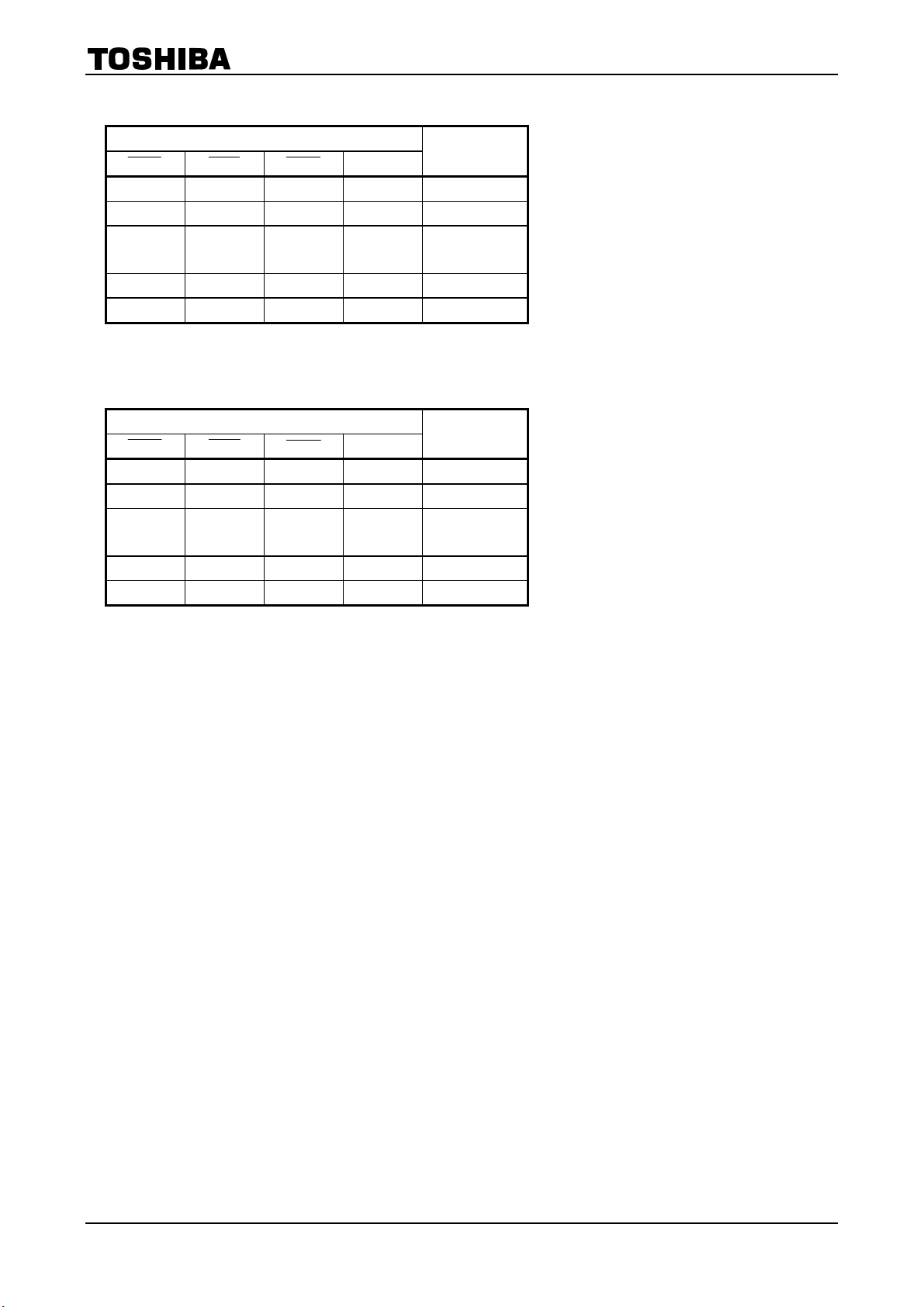
data from A or to output data from B. If CEAB is low and LEAB is low, the A-to-B latches are transparent; a
subsequent low-to-high transition of LEAB puts the A latches in the storage mode. With CEAB and OEAB both low,
the 3-state B outputs are active and reflect the data present at the output of the A latches.
Data flow from B to A is similar but requires using the CEBA, LEBA, and OEAB inputs.
When the OE
3-state memory address drivers, etc.
All inputs are equipped with protection circuits against static discharge.
input is high, the outputs are in a high-impedance state. This device is designed to be used with
Features (Note)
Weight: 0.25 g (typ.)
• Low-voltage operation: VCC = 1.8 to 3.6 V
• High-speed operation: t
: t
: tpd = 8.0 ns (max) (VCC = 1.8 V)
• Output current: I
: I
: I
• Latch-up performance: −300 mA
• ESD performance: Machine model ≥ ±200 V
Human body model ≥ ±2000 V
• Package: TSSOP
• Bidirectional interface between 2.5 V and 3.3 V signals.
• 3.6-V tolerant function and power-down protection provided on all inputs and outputs
Note: Do not apply a signal to any bus pins when it is in the output mode. Damage may result.
All floating (high impedance) bus pins must have their input level fixed by means of pull-up or pull-down
resistors.
OH/IOL
OH/IOL
OH/IOL
= 3.5 ns (max) (VCC = 3.0 to 3.6 V)
pd
= 4.0 ns (max) (VCC = 2.3 to 2.7 V)
pd
= ±24 mA (min) (VCC = 3.0 V)
= ±18 mA (min) (VCC = 2.3 V)
= ±6 mA (min) (VCC = 1.8 V)
1
2007-10-19

TC74VCX16543FT
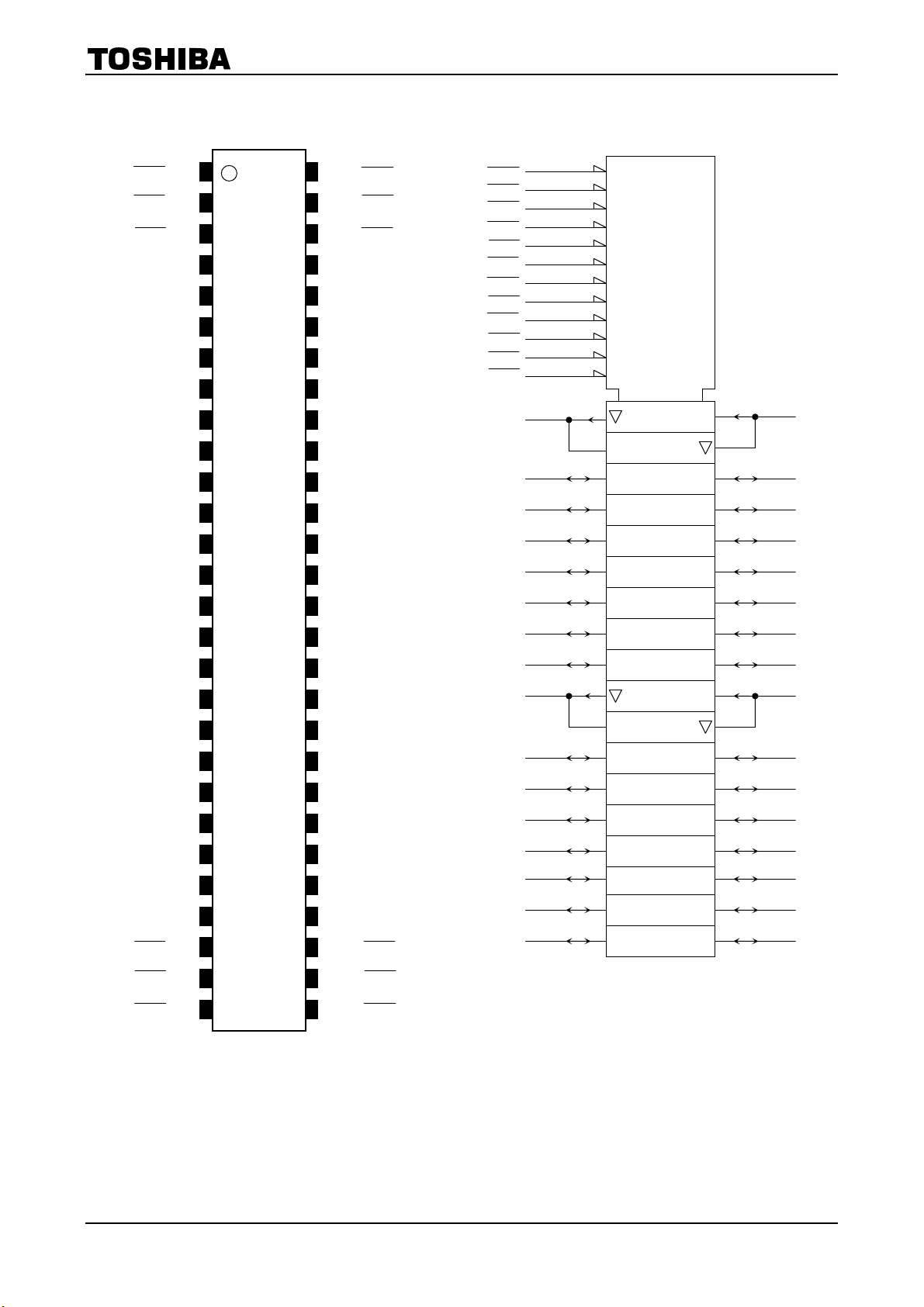
Pin Assignment
1
OEAB1
LEAB1
CEAB1
2
3
4
GND
5
1A1
6
1A2
7
V
CC
1A3
8
1A4
9
10
1A5
GND 11
1A6
12
1A7
13
14
1A8
15
2A1
16
2A2
17
2A3
18
GND
(top view)
IEC Logic Symbol
1A1
1A2
1A3
1A4
1A5
1A6
1A7
1A8
2A1
56
54
55
29
31
30
28
26
27
10
12
13
14
15
1EN3
G1
C5
1
3
2
2EN4
G2
2C6
7EN9
G7
7C11
8EN10
G8
8C12
5
35D
6
8
9
56
55
54
53
52
51
50
49
48
47
46
45
44
43
42
41
40
39
OEBA1
LEBA1
CEBA1
GND
1B1
1B2
V
CC
1B3
1B4
1B5
GND
1B6
1B7
1B8
2B1
2B2
2B3
GND
OEBA1
CEBA1
LEBA1
OEAB1
CEAB1
LEAB1
OEBA2
CEBA2
LEBA2
OEAB2
CEAB2
LEAB2
52
1B1
4 6D
51
1B2
49
1B3
48
1B4
47
1B5
45
1B6
44
1B7
43
1B8
11D9
42
2B1
19
2A4
20
2A5
21
2A6
22
V
CC
2A7
23
24
2A8
25 GND
26
CEAB2
27 LEAB2
28
OEAB2
38
37
36
35
34
33
32
31
30
29
2B4
2B5
2B6
VCC
2B7
2B8
GND
CEBA2
LEBA2
OEBA2
16
2A2
17
2A3
19
2A4
20
2A5
21
2A6
23
2A7
24
2A8
10 12D
41
2B2
40
2B3
38
2B4
37
2B5
36
2B6
34
2B7
33
2B8
2
2007-10-19

TC74VCX16543FT
Truth Table
CEAB LEAB OEAB A
H X X X Z
X X H X Z
L H L X
L L L L L
L L L H H
Note: Output level before the indicated steady-state input conditions were established.
Truth Table
CEBA LEBA OEBA B
H X X X Z
X X H X Z
L H L X
L L L L L
L L L H H
(A bus → B bus each 8-bit latch)
Inputs
(B bus → A bus each 8-bit latch)
Inputs
Outputs
B
B0
(Note)
Outputs
A
A0
(Note)
Note: Output level before the indicated steady-state input conditions were established.
3
2007-10-19

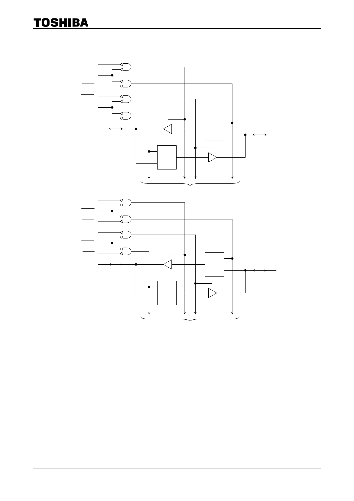
System Diagram
OEBA1
CEBA1
LEBA1
OEAB1
CEAB1
LEAB1
OEBA2
CEBA2
LEBA2
OEAB2
CEAB2
LEAB2
1A1
2A1
56
54
55
29
31
30
28
26
27
15
TC74VCX16543FT
1
3
2
5
LE
D
To seven other channels
LE
LE
52
42
1B1
2B1
D
D
LE
D
To seven other channels
4
2007-10-19
 Loading...