TC74VCX16373FT
TOSHIBA CMOS Digital Integrated Circuit Silicon Monolithic
TC74VCX16373FT
Low-Voltage 16-Bit D-Type Latch with 3.6-V Tolerant Inputs and Outputs
The TC74VCX16373FT is a high-performance CMOS 16-bit
D-type latch. Designed for use in 1.8-V, 2.5-V or 3.3-V systems, it
achieves high-speed operation while maintaining the CMOS low
power dissipation.
It is also designed with overvoltage tolerant inputs and outputs
up to 3.6 V.
This 16-bit D-type latch is controlled by a latch enable input
(LE) and an output enable input (OE) which are common to each
byte. It can be used as two 8-bit latches or one 16-bit latch. When
the OE input is high, the outputs are in a high-impedance state.
All inputs are equipped with protection circuits against static
discharge.
Features
Weight: 0.25 g (typ.)
• Low-voltage operation: VCC = 1.8 to 3.6 V
• High-speed operation : t
: t
: tpd = 5.7 ns (max) (VCC = 1.8 V)
• Output current : I
: I
: IOH/IOL = ±6 mA (min) (VCC = 1.8 V)
• Latch-up performance: −300 mA
• ESD performance: Machine model ≥ ±200 V
Human body model ≥ ±2000 V
• Package: TSSOP
• 3.6-V tolerant function and power-down protection provided on all inputs and outputs
OH/IOL
OH/IOL
= 3.0 ns (max) (VCC = 3.0 to 3.6 V)
pd
= 3.4 ns (max) (VCC = 2.3 to 2.7 V)
pd
= ±24 mA (min) (VCC = 3.0 V)
= ±18 mA (min) (VCC = 2.3 V)
1
2007-10-19

TC74VCX16373FT
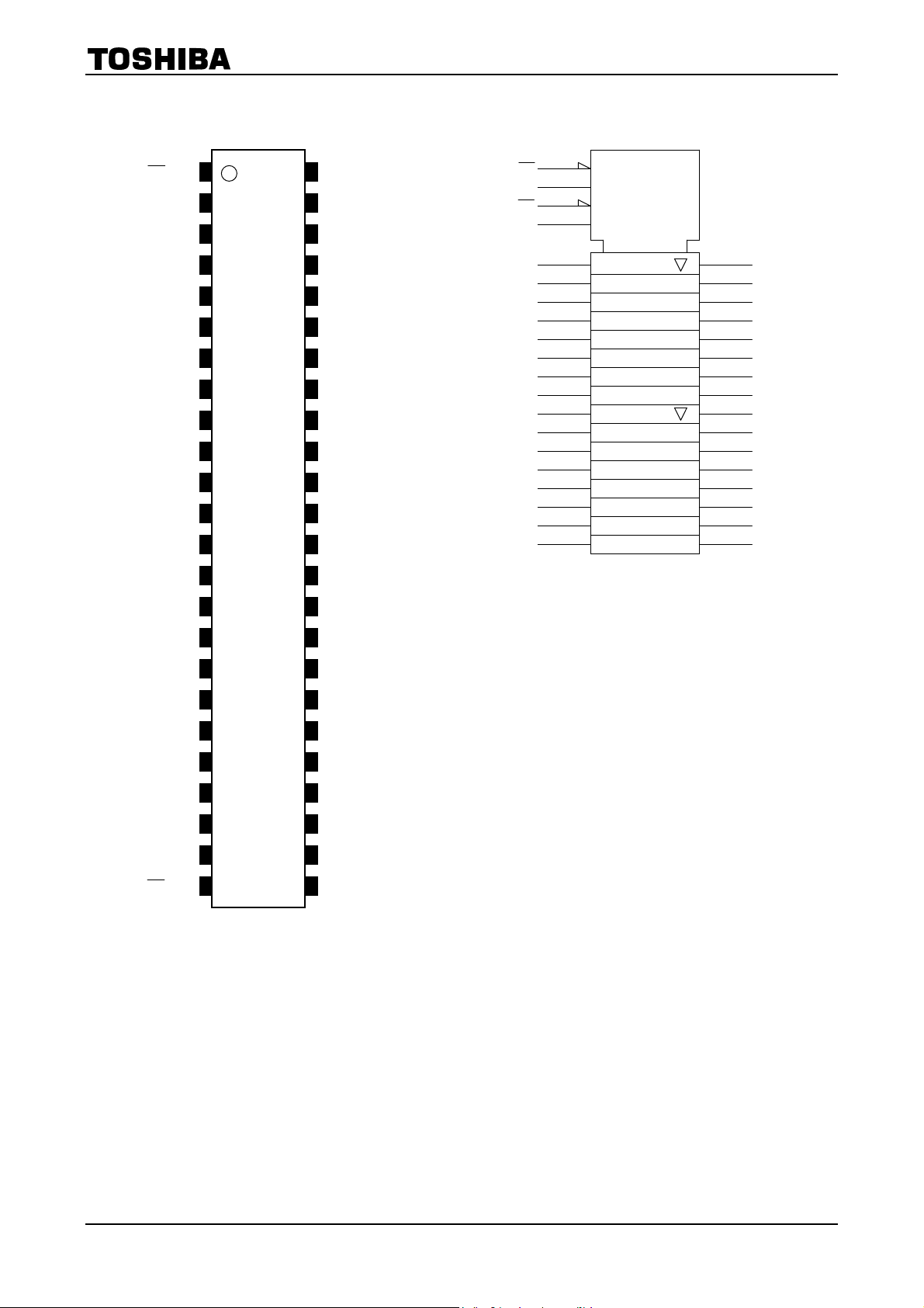
Pin Assignment
1
OE1
1Q1
2
1Q2
3
4
GND
5
1Q3
6
1Q4
V
7
CC
1Q5
8
1Q6
9
10
GND
11
1Q7
12
1Q8
13
2Q1
(top view)
IEC Logic Symbol
1
48
24
25
47
46
44
43
41
40
38
37
36
35
33
32
30
29
27
26
1EN
C3
2EN
C4
4D 2
47
46
45
44
43
42
41
40
39
38
37
36
1LE 48
1D1
1D2
GND
1D3
1D4
V
CC
1D5
1D6
GND
1D7
1D8
2D1
OE1
1LE
OE2
2LE
1D1 3D 1
1D2
1D3
1D4
1D5
1D6
1D7
1D8
2D1
2D2
2D3
2D4
2D5
2D6
2D7
2D8
2
1Q1
3
1Q2
5
1Q3
6
1Q4
8
1Q5
9
1Q6
11
1Q7
12
1Q8
13
2Q1
14
2Q2
16
2Q3
17
2Q4
19
2Q5
20
2Q6
22
2Q7
23
2Q8
2Q2
GND
2Q3
2Q4
V
CC
2Q5
2Q6
2Q7
2Q8
OE2
14
15
16
17
18
19
20
21 GND
22
23
24
35
34
33
32
31
30
29
28
27
26
25
2D2
GND
2D3
2D4
VCC
2D5
2D6
GND
2D7
2D8
2LE
2
2007-10-19

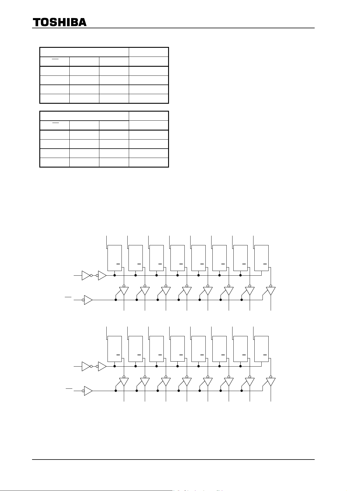
Truth Table
OE1 1LE 1D1-1D8 1Q1-1Q8
H X X Z
L L X Qn
L H L L
L H H H
OE2 2LE 2D1-2D8 2Q1-2Q8
H X X Z
L L X Qn
L H L L
L H H H
X: Don’t care
Z: High impedance
TC74VCX16373FT
Inputs Outputs
Inputs Outputs
Qn: Q outputs are latched at the time when the LE input is taken to a low logic level.
System Diagram
1D1
47
48
1LE
1
OE1
2D1
36
25
2LE
1D2
46 44 43 41 40 38 37
D
LE
Q
2
1Q1
2D2
35 33 32 30 29 27 26
D
LE
Q
D
LE
D
LE
Q
Q
3
1Q2
1D3
2D3
LE
LE
1D4
D
Q
5
1Q3
2D4
D
Q
LE
LE
1D5
D
Q
6
1Q4
2D5
D
Q
LE
LE
1D6
D
D
Q
Q
D
LE
8
1Q5
2D6
D
LE
Q
Q
9
1Q6
1D7
2D7
LE
LE
1D8
D
D
Q
11
Q
1Q7
2D8
D
LE
D
LE
Q
12
1Q8
Q
24
OE2
13
2Q1
14
2Q2
16
2Q3
17
2Q4
3
19
2Q5
20
2Q6
22
2Q7
23
2Q8
2007-10-19

TC74VCX16373FT
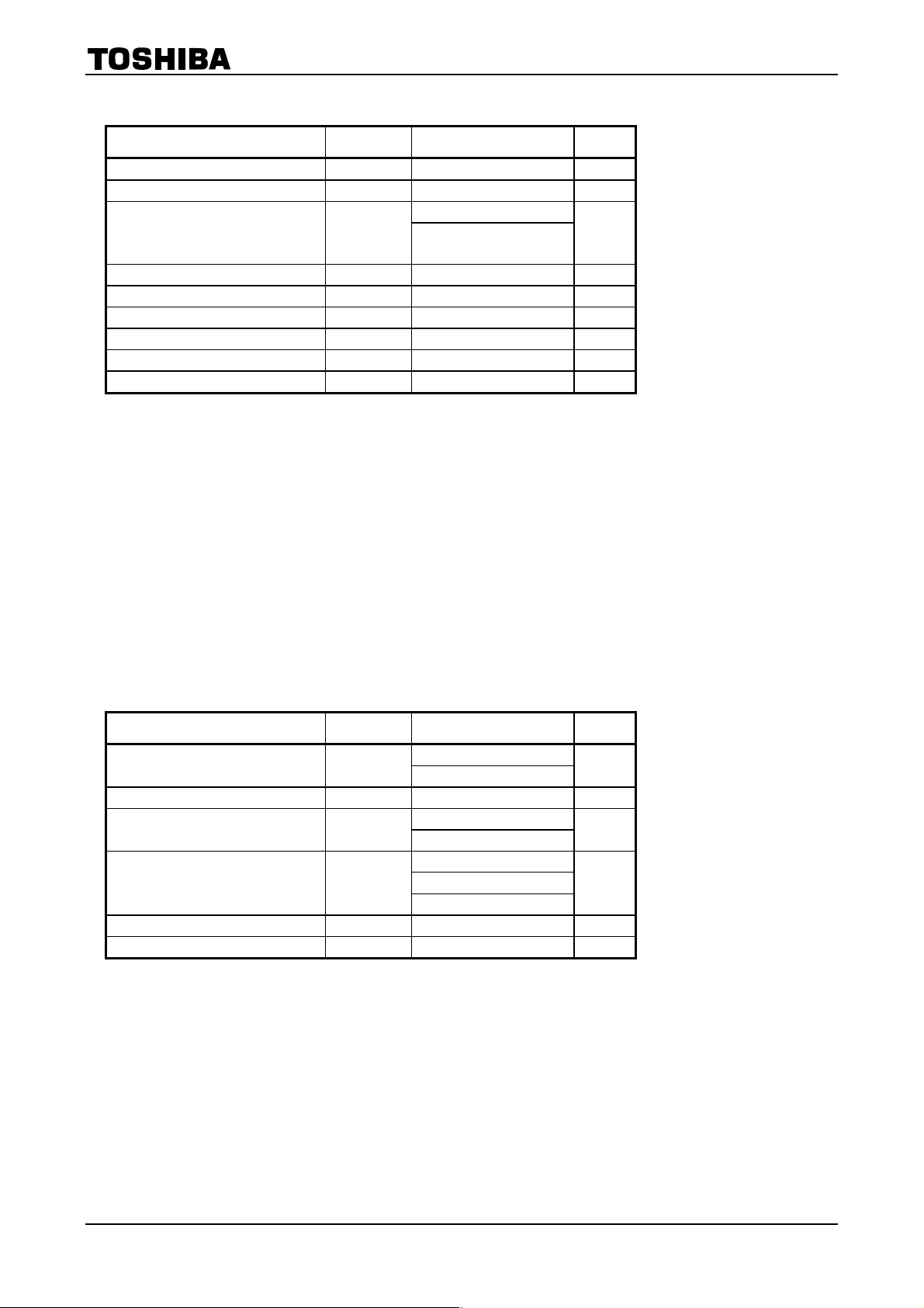
Absolute Maximum Ratings (Note 1)
Characteristics Symbol Rating Unit
Power supply voltage V
DC input voltage V
DC output voltage V
Input diode current I
Output diode current I
DC output current I
Power dissipation P
DC VCC/ground current per supply pin ICC/I
Storage temperature T
CC
IN
OUT
IK
OK
OUT
D
stg
−0.5 to 4.6 (Note 2)
−0.5 to V
(Note 3)
±50 (Note 4) mA
GND
Note 1: Exceeding any of the absolute maximum ratings, even briefly, lead to deterioration in IC performance or
even destruction.
Using continuously under heavy loads (e.g. the application of high temperature/current/voltage and the
significant change in temperature, etc.) may cause this product to decrease in the reliability significantly
even if the operating conditions (i.e. operating temperature/current/voltage, etc.) are within the absolute
maximum ratings and the operating ranges.
Please design the appropriate reliability upon reviewing the Toshiba Semiconductor Reliability Handbook
(“Handling Precautions”/“Derating Concept and Methods”) and individual reliability data (i.e. reliability test
report and estimated failure rate, etc).
−0.5 to 4.6 V
−0.5 to 4.6 V
+ 0.5
CC
−50 mA
±50 mA
400 mW
±100 mA
−65 to 150 °C
V
Note 2: OFF state
Note 3: High or low state. I
Note 4: V
OUT
< GND, V
absolute maximum rating must be observed.
OUT
> VCC
OUT
Operating Ranges (Note 1)
Characteristics Symbol Rating Unit
Power supply voltage V
Input voltage V
Output voltage V
Output current IOH/IOL
Operating temperature T
Input rise and fall time dt/dv 0 to 10 (Note 8) ns/V
CC
IN
OUT
opr
1.2 to 3.6 (Note 2)
0 to 3.6 (Note 3)
0 to VCC (Note 4)
±24 (Note 5)
±18 (Note 6)
1.8 to 3.6
−0.3 to 3.6 V
±6 (Note 7)
−40 to 85 °C
Note 1: The operating ranges must be maintained to ensure the normal operation of the device.
Unused inputs must be tied to either VCC or GND.
Note 2: Data retention only
V
V
mA
Note 3: OFF state
Note 4: High or low state
Note 5: V
= 3.0 to 3.6 V
CC
Note 6: VCC = 2.3 to 2.7 V
Note 7: VCC = 1.8 V
Note 8: VIN = 0.8 to 2.0 V, VCC = 3.0 V
4
2007-10-19
 Loading...