TC74VCX14FT/FK
TOSHIBA CMOS Digital Integrated Circuit Silicon Monolithic
TC74VCX14FT,TC74VCX14FK
Low-Voltage Hex Schmitt Inverter with 3.6-V Tolerant Inputs and Outputs
The TC74VCX14FT/FK is a high-performance CMOS schmitt
inverter which is guaranteed to operate from 1.2-V to 3.6-V.
Designed for use in 1.5V, 1.8V, 2.5V or 3.3V systems, it achieves
high-speed operation while maintaining the CMOS low power
dissipation.
It is also designed with over-voltage tolerant inputs and
outputs up to 3.6 V.
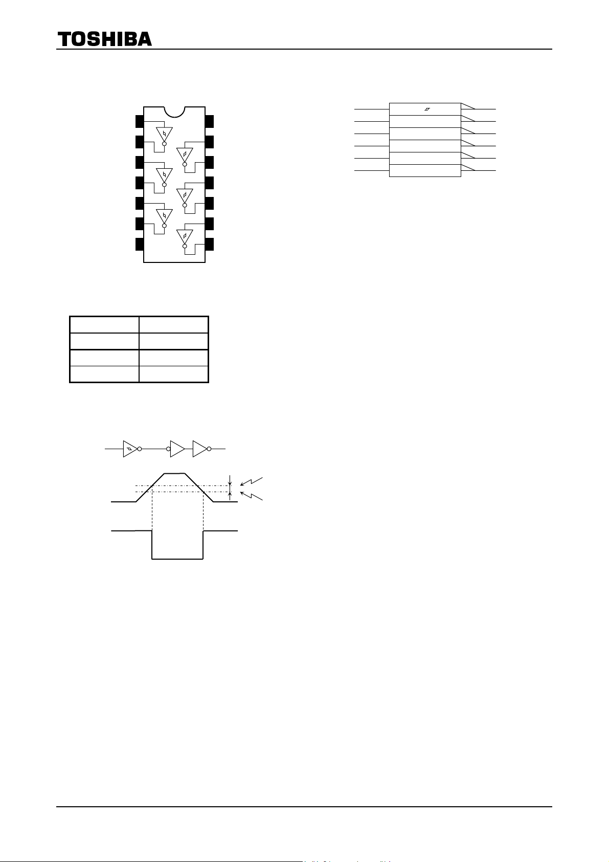
Pin configuration and function are the same as the
TC74VCX04 but the inputs have hysteresis and with its schmitt
trigger function, the TC74VCX14 can be used as a line receivers
which will receive slow input signals.
All inputs are equipped with protection circuits against static
discharge.
Features
TC74VCX14FT
TC74VCX14FK
• Low-voltage operation: VCC = 1.2~3.6 V
• High-speed operation : t
: t
: tpd = 8.6 ns (max) (VCC = 1.65~1.95 V)
: t
: t
• Output current : IOH/IOL = ±24 mA (min) (VCC = 3.0 V)
: I
: I
: I
• Latch-up performance: −300 mA
• ESD performance: Machine model ≥ ±200 V
Human body model ≥ ±2000 V
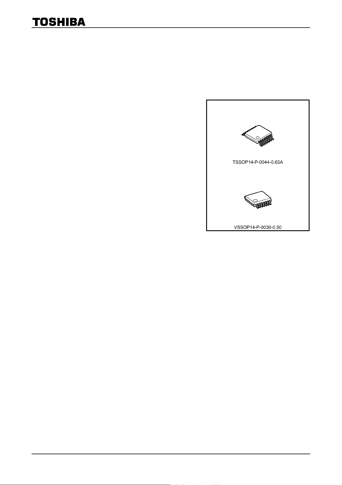
• Package: TSSOP and VSSOP (US)
• Power-down protection provided on all inputs and outputs
OH/IOL
OH/IOL
OH/IOL
= 4.0 ns (max) (VCC = 3.0~3.6 V)
pd
= 4.3 ns (max) (VCC = 2.3~2.7 V)
pd
= 17.2 ns (max) (VCC = 1.4~1.6 V)
pd
= 43.0 ns (max) (VCC = 1.2 V)
pd
= ±18 mA (min) (VCC = 2.3 V)
= ±6 mA (min) (VCC = 1.65 V)
= ±2 mA (min) (VCC = 1.4 V)
Weight
TSSOP14-P-0044-0.65A : 0.06 g (typ.)
VSSOP14-P-0030-0.50 : 0.02 g (typ.)
1
2007-10-19

TC74VCX14FT/FK
Pin Assignment
(top view)
IEC Logic Symbol
1A 1
1Y
2A
2Y
3A
3Y
GND
2
3
4
5
6
7
14
13
12
11
10
9
8
V
6A
6Y
5A
5Y
4A
4Y
Truth Table
Inputs Outputs
A Y
L H
H L
System Diagram and Waveforms
CC
1A
2A
3A
4A
5A
6A
(1)
(3)
(5)
(9)
(11)
(13)
(2)
1Y
(4)
2Y
(6)
3Y
(8)
4Y
(10)
5Y
(12)
6Y
Y
V
H
V
P
V
N
V
V
OUT
A
(A)
IN
(Y)
2
2007-10-19

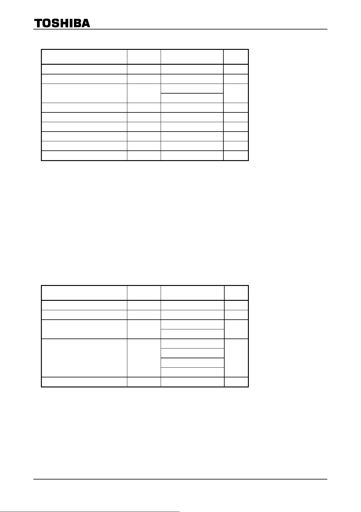
Absolute Maximum Ratings (Note 1)
Characteristics Symbol Rating Unit
TC74VCX14FT/FK
Power supply voltage V
DC input voltage V
DC output voltage V
Input diode current I
Output diode current I
DC output current I
Power dissipation P
DC VCC/ground current ICC/I
Storage temperature T
CC
IN
OUT
IK
OK
OUT
D
GND
stg
−0.5~4.6 (Note 2)
±50 (Note 4) mA
−0.5~4.6 V
−0.5~4.6 V
V
−0.5~VCC + 0.5 (Note 3)
−50 mA
±50 mA
180 mW
±100 mA
−65~150 °C
Note 1: Exceeding any of the absolute maximum ratings, even briefly, lead to deterioration in IC performance or
even destruction.
Using continuously under heavy loads (e.g. the application of high temperature/current/voltage and the
significant change in temperature, etc.) may cause this product to decrease in the reliability significantly
even if the operating conditions (i.e. operating temperature/current/voltage, etc.) are within the absolute
maximum ratings and the operating ranges.
Please design the appropriate reliability upon reviewing the Toshiba Semiconductor Reliability Handbook
(“Handling Precautions”/“Derating Concept and Methods”) and individual reliability data (i.e. reliability test
report and estimated failure rate, etc).
Note 2: V
Note 3: High or low state. I
Note 4: V
CC
OUT
= 0 V
<
GND, V
absolute maximum rating must be observed.
OUT
>
VCC
OUT
Operating Ranges (Note 1)
Characteristics Symbol Rating Unit
Power supply voltage V
Input voltage V
Output voltage V
Output current IOH/IOL
Operating temperature T
CC
IN
OUT
opr
0~3.6 (Note 2)
0~VCC (Note 3)
±24 (Note 4)
±18 (Note 5)
±6 (Note 6)
±2 (Note 7)
1.2~3.6 V
−0.3~3.6 V
V
mA
−40~85 °C
Note 1: The operating ranges must be maintained to ensure the normal operation of the device.
Unused inputs must be tied to either VCC or GND.
Note 2: V
CC
= 0 V
Note 3: High or low state
Note 4: VCC = 3.0~3.6 V
Note 5: VCC = 2.3~2.7 V
Note 6: VCC = 1.65~1.95 V
Note 7: VCC = 1.4~1.6 V
3
2007-10-19

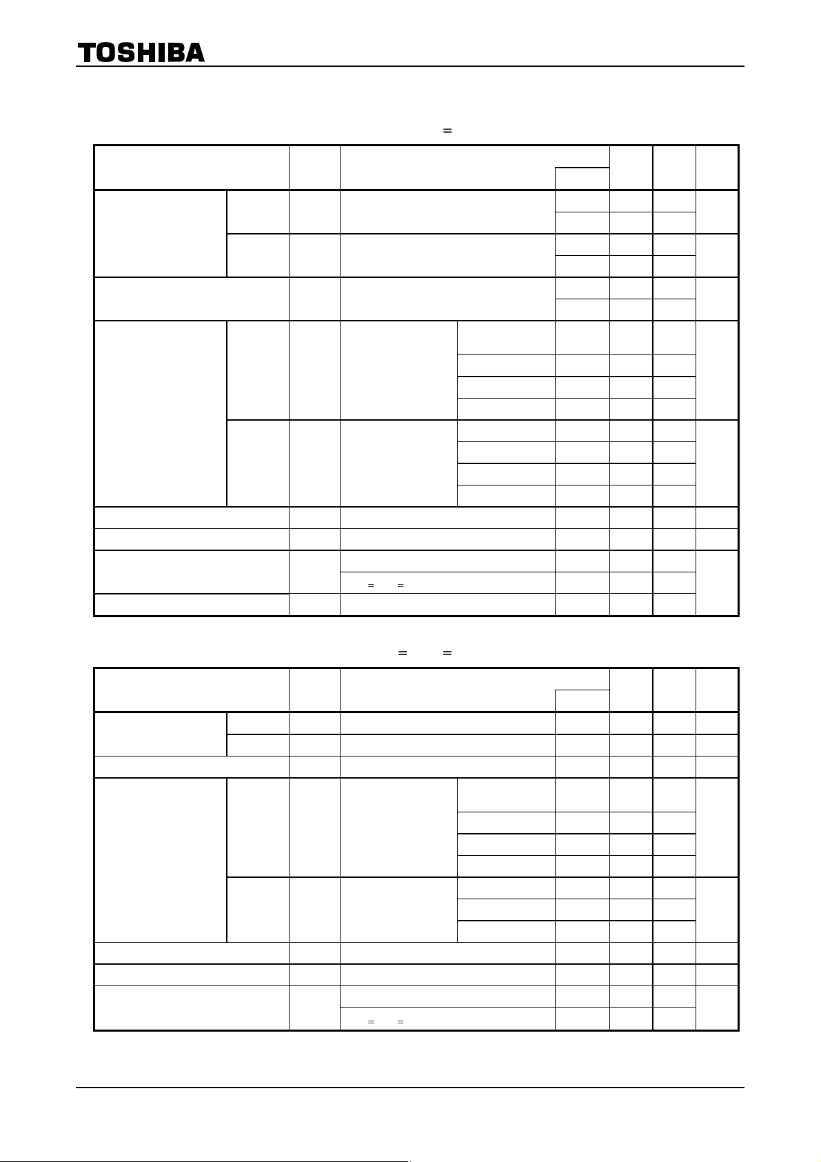
Electrical Characteristics
<
<
<
<
<
<
<
TC74VCX14FT/FK
DC Characteristics
Characteristics Symbol Test Condition
Input voltage
Hysteresis voltage VH ⎯
Output voltage
Input leakage current I
Power-off leakage current I
Quiescent supply current ICC
Increase in ICC per input ΔICC VIH = VCC − 0.6 V 2.7~3.6 ⎯ 750
(Ta = −40 to 85°C, 2.7 V < V
H-level
L-level V
H-level
L-level VOL VIN = VIH
VP ⎯
⎯
N
VOH VIN = VIL
VIN = 0 to 3.6 V 2.7~3.6 ⎯ ±5.0 μA
IN
VIN, V
OFF
VIN = VCC or GND 2.7~3.6 ⎯ 20.0
V
CC
= 0 to 3.6 V 0 ⎯ 10.0 μA
OUT
V
3.6 V 2.7~3.6 ⎯ ±20.0
IN
CC
3.6 V)
Min Max Unit
(V)
V
CC
3.6 ⎯ 2.2
3.0 ⎯ 2.0
3.6 0.8 ⎯
3.0 0.7 ⎯
3.6 0.3 1.2
3.0 0.3 1.2
V
IOH = −100 μA 2.7~3.6
IOH = −12 mA 2.7 2.2 ⎯
IOH = −18 mA 3.0 2.4 ⎯
I
= −24 mA 3.0 2.2 ⎯
OH
IOL = 100 μA 2.7~3.6 ⎯ 0.2
IOL = 12 mA 2.7 ⎯ 0.4
IOL = 18 mA 3.0 ⎯ 0.4
I
= 24 mA 3.0 ⎯ 0.55
OL
CC
− 0.2
DC Characteristics
(Ta = −40 to 85°C, 2.3 V
V
CC
2.7 V)
V
V
V
⎯
V
V
μA
Characteristics Symbol Test Condition
H-level
Input voltage
Hysteresis voltage VH ⎯ 2.3 0.3 1.0 V
Output voltage
Input leakage current I
Power-off leakage current I
Quiescent supply current ICC
L-level V
H-level
L-level VOL VIN = VIH
VP ⎯ 2.3 ⎯ 1.6 V
⎯ 2.3 0.5 ⎯ V
N
IOH = −100 μA 2.3~2.7
VOH VIN = VIL
VIN = 0 to 3.6 V 2.3~2.7 ⎯ ±5.0 μA
IN
VIN, V
OFF
VIN = VCC or GND 2.3~2.7 ⎯ 20.0
V
CC
= 0 to 3.6 V 0 ⎯ 10.0 μA
OUT
V
3.6 V 2.3~2.7 ⎯ ±20.0
IN
IOH = −6 mA 2.3 2.0 ⎯
IOH = −12 mA 2.3 1.8 ⎯
I
= −18 mA 2.3 1.7 ⎯
OH
IOL = 100 μA 2.3~2.7 ⎯ 0.2
IOL = 12 mA 2.3 ⎯ 0.4
= 18 mA 2.3 ⎯ 0.6
I
OL
V
CC
Min Max Unit
(V)
V
CC
− 0.2
⎯
V
V
μA
4
2007-10-19
 Loading...