

TC74LCX04F/FN/FT/FK
TOSHIBA CMOS Digital Integrated Circuit Silicon Monolithic
TC74LCX04F,TC74LCX04FN,TC74LCX04FT,TC74LCX04FK
Low-Voltage Hex Inverter with 5-V Tolerant Inputs and Outputs
The TC74LCX04 is a high-performance CMOS inverter.
Designed for use in 3.3-V systems, it achieves high-speed
operation while maintaining the CMOS low power dissipation.
The device is designed for low-voltage (3.3 V) V
but it could be used to interface to 5-V supply environment for
inputs.
All inputs are equipped with protection circuits against static
discharge.
applications,
CC
Features
• Low-voltage operation: V
• High-speed operation: t
• Output current: |IOH|/I
• Latch-up performance: >±500 mA
• Available in JEDEC SOP, JEITA SOP, TSSOP and
VSSOP (US)
• Power-down protection provided on all inputs and outputs
• Pin and function compatible with the 74 series
(74AC/VHC/HC/F/ALS/LS etc.) 04 type
Note: The Electrical Characteristics of V
from January 2009 onward.
= 1.65 to 3.6 V
CC
= 5.2 ns (max) (V
pd
= 24 mA (min) (V
OL
= 3.0 to 3.6 V)
CC
= 3.0 V)
CC
=1.8±0.15V is only applicable for products which manufactured
CC
Note: xxxFN (JEDEC SOP) is not available in
Japan.
TC74LCX04F
TC74LCX04FN
TC74LCX04FT
TC74LCX04FK
Weight
SOP14-P-300-1.27A : 0.18 g (typ.)
SOL14-P-150-1.27 : 0.12 g (typ.)
TSSOP14-P-0044-0.65A : 0.06 g (typ.)
VSSOP14-P-0030-0.50 : 0.02 g (typ.)
1
2010-01-31
TC74LCX04F/FN/FT/FK
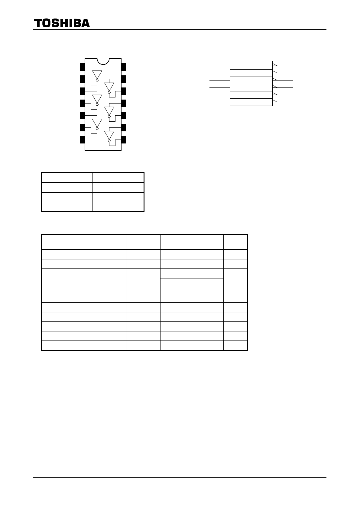
Pin Assignment
(top view)
IEC Logic Symbol
V
1A 1
1Y
2A
2Y
3A
3Y
GND
2
3
4
5
6
7
14
13
12
11
10
9
8
CC
6A
6Y
5A
5Y
4A
4Y
Truth Table
Inputs Outputs
A Y
L H
H L
Absolute Maximum Ratings (Note 1)
1A
2A
3A
4A
5A
6A
11
13
1
3
5
9
1
2
4
6
8
10
12
1Y
2Y
3Y
4Y
5Y
6Y
Characteristics Symbol Rating Unit
Power supply voltage V
DC input voltage V
DC output voltage V
Input diode current I
Output diode current I
DC output current I
Power dissipation P
DC VCC/ground current ICC/I
Storage temperature T
CC
IN
OUT
IK
OK
OUT
D
GND
stg
−0.5 to 7.0 (Note 2)
±50 (Note 4) mA
−0.5 to 7.0 V
−0.5 to 7.0 V
−0.5 to VCC + 0.5
(Note 3)
−50 mA
±50 mA
180 mW
±100 mA
−65 to 150 °C
V
Note 1: Exceeding any of the absolute maximum ratings, even briefly, lead to deterioration in IC performance or
even destruction.
Using continuously under heavy loads (e.g. the application of high temperature/current/voltage and the
significant change in temperature, etc.) may cause this product to decrease in the reliability significantly
even if the operating conditions (i.e. operating temperature/current/voltage, etc.) are within the absolute
maximum ratings and the operating ranges.
Please design the appropriate reliability upon reviewing the Toshiba Semiconductor Reliability Handbook
(“Handling Precautions”/“Derating Concept and Methods”) and individual reliability data (i.e. reliability test
report and estimated failure rate, etc).
Note 2: V
Note 3: High or low state. I
Note 4: V
CC
OUT
= 0 V
< GND, V
absolute maximum rating must be observed.
OUT
> VCC
OUT
2
2010-01-31
Operating Ranges (Note 1)
Characteristics Symbol Rating Unit
TC74LCX04F/FN/FT/FK
Power supply voltage V
Input voltage V
Output voltage V
Output current IOH/IOL
Operating temperature T
Input rise and fall time dt/dv 0 to 10 (Note 7) ns/V
CC
IN
OUT
opr
1.5 to 3.6 (Note 2)
0 to 5.5 (Note 3)
0 to VCC (Note 4)
±24 (Note 5)
±12 (Note 6)
1.65 to 3.6
0 to 5.5 V
−40 to 85 °C
V
V
mA
Note 1: The operating ranges must be maintained to ensure the normal operation of the device.
Unused inputs must be tied to either V
or GND.
CC
Note 2: Data retention only
Note 3: V
Note 4: High or low state ( However, it can not exceed I
CC
= 0 V
of absolute maximum ratings. )
OUT
Note 5: VCC = 3.0 to 3.6 V
Note 6: VCC = 2.7 to 3.0 V
Note 7: VIN = 0.8 to 2.0 V, VCC = 3.0 V
3
2010-01-31
Electrical Characteristics
TC74LCX04F/FN/FT/FK
DC Characteristics
Characteristics Symbol Test Condition
Input voltage
Output voltage
Input leakage current I
Power-off leakage current I
Quiescent supply current ICC
Increase in Icc per input ΔICC VIH = VCC − 0.6 V 2.7 to 3.6 ⎯ 500
(Ta = −40 to 85°C)
H-level
L-level V
H-level
L-level VOL VIN = VIH
VIH ⎯
⎯
IL
V
V
OH
IN
VIN/V
OFF
= VIL
IN
VIN = 0 to 5.5 V 1.65 to 3.6 ⎯ ±5.0 μA
= 5.5 V 0 ⎯ 10.0 μA
OUT
VIN = VCC or GND 1.65 to 3.6 ⎯ 10.0
V
= 3.6 to 5.5 V 1.65 to 3.6 ⎯ ±10.0
IN
(V)
V
CC
1.65 to 2.3 VCC×0.9 ⎯
2.3 to 2.7 1.7 ⎯
2.7 to 3.6 2.0 ⎯
1.65 to 2.3 ⎯ VCC×0.1
2.3 to 2.7 ⎯ 0.7
2.7 to 3.6 ⎯ 0.8
IOH = −100 μA 1.65 to 3.6 VCC−0.2 ⎯
IOH = −4 mA 1.65 1.05 ⎯
IOH = −8 mA 2.3 1.7 ⎯
IOH = −12 mA 2.7 2.2 ⎯
IOH = −18 mA 3.0 2.4 ⎯
= −24 mA 3.0 2.2 ⎯
I
OH
IOL = 100 μA 1.65 to 3.6 ⎯ 0.2
IOL = 4 mA 1.65 ⎯ 0.45
IOL = 8 mA 2.3 ⎯ 0.7
IOL = 12 mA 2.7 ⎯ 0.4
IOL = 16 mA 3.0 ⎯ 0.4
= 24 mA 3.0 ⎯ 0.55
I
OL
Min Max Unit
V
V
μA
4
2010-01-31
TC74LCX04F/FN/FT/FK
AC Characteristics
Characteristics Symbol Test Condition
Propagation delay time
Output to output skew
(Ta = −40 to 85°C)
Note: Parameter guaranteed by design.
(t
osLH
= |t
pLHm
− t
pLHn
|, t
osHL
Dynamic Switching Characteristics
Characteristics Symbol Test Condition
Quiet output maximum dynamic V
Quiet output minimum dynamic VOL |V
Capacitive Characteristics
OL
(Ta = 25°C)
(V)
V
CC
1.8 ± 0.15 ⎯ 20.0
t
pLH
t
pHL
t
osLH
t
osHL
= |t
Figure 1, Figure 2
− t
pHLm
pHLn
(Note)
|)
2.5 ± 0.2 ⎯ 7.0
2.7 ⎯ 6.0
3.3 ± 0.3 1.5 5.2
2.7 ⎯ ⎯
3.3 ± 0.3 ⎯ 1.0
(Ta = 25°C, input: tr = tf = 2.5 ns, CL = 50 pF, RL = 500 Ω)
V
VIH = 3.3 V, VIL = 0 V 3.3 0.8 V
OLP
| VIH = 3.3 V, VIL = 0 V 3.3 0.8 V
OLV
Min Max Unit
(V)
V
CC
ns
ns
Typ. Unit
Characteristics Symbol Test Condition
Input capacitance
Output capacitance
Power dissipation capacitance CPD fIN = 10 MHz (Note) 3.3 25 pF
CIN ⎯ 3.3 7 pF
C
⎯ 0 8 pF
OUT
V
CC
Typ. Unit
(V)
Note: CPD is defined as the value of the internal equivalent capacitance which is calculated from the operating
current consumption without load.
Average operating current can be obtained by the equation:
I
CC (opr)
= CPD・VCC・fIN + ICC/6 (per gate)
5
2010-01-31

AC Test Circuit
AC Waveform
Input
Output
Output
L
C
Figure 1
tf tr
t
pLH
10%
L
R
Measure
90%
V
IM
V
t
pHL
OM
TC74LCX04F/FN/FT/FK
V
IH
GND
V
OH
V
OL
Figure 2 t
pLH
, t
pHL
VCC
Symbol
Input
Output VOM 1.5V VOH/2 VOH/2
VIH 2.7V VCC V
VIM 1.5V VCC/2 VCC/2
tr,tf 2.5ns 2.0ns 2.0ns
CL 50pF 30pF 30pF Load
R
L
3.3 ± 0.3 V
2.7V
500Ω 500Ω 1kΩ
2.5 ± 0.2 V 1.8 ± 0.15 V
CC
6
2010-01-31

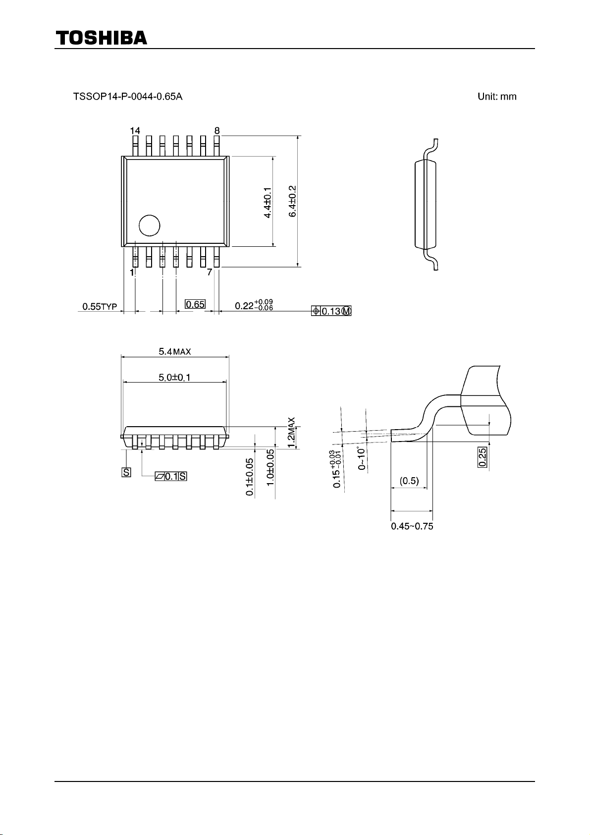
Package Dimensions
TC74LCX04F/FN/FT/FK
Weight: 0.18 g (typ.)
7
2010-01-31

Package Dimensions (Note)
TC74LCX04F/FN/FT/FK
Note: This package is not available in japan.
Weight: 0.12 g (typ.)
8
2010-01-31
Package Dimensions
TC74LCX04F/FN/FT/FK
Weight: 0.06 g (typ.)
9
2010-01-31

Package Dimensions
TC74LCX04F/FN/FT/FK
Weight: 0.02 g (typ.)
10
2010-01-31

TC74LCX04F/FN/FT/FK
RESTRICTIONS ON PRODUCT USE
• Toshiba Corporation, and its subsidiaries and affiliates (collectively “TOSHIBA”), reserve the right to make changes to the information
in this document, and related hardware, software and systems (collectively “Product”) without notice.
• This document and any information herein may not be reproduced without prior written permission from TOSHIBA. Even with
TOSHIBA’s written permission, reproduction is permissible only if reproduction is without alteration/omission.
• Though TOSHIBA works continually to improve Product’s quality and reliability, Product can malfunction or fail. Customers are
responsible for complying with safety standards and for providing adequate designs and safeguards for their hardware, software and
systems which minimize risk and avoid situations in which a malfunction or failure of Product could cause loss of human life, bodily
injury or damage to property, including data loss or corruption. Before customers use the Product, create designs including the
Product, or incorporate the Product into their own applications, customers must also refer to and comply with (a) the latest versions of
all relevant TOSHIBA information, including without limitation, this document, the specifications, the data sheets and application notes
for Product and the precautions and conditions set forth in the “TOSHIBA Semiconductor Reliability Handbook” and (b) the
instructions for the application with which the Product will be used with or for. Customers are solely responsible for all aspects of their
own product design or applications, including but not limited to (a) determining the appropriateness of the use of this Product in such
design or applications; (b) evaluating and determining the applicability of any information contained in this document, or in charts,
diagrams, programs, algorithms, sample application circuits, or any other referenced documents; and (c) validating all operating
parameters for such designs and applications. TOSHIBA ASSUMES NO LIABILITY FOR CUSTOMERS’ PRODUCT DESIGN OR
APPLICATIONS.
• Product is intended for use in general electronics applications (e.g., computers, personal equipment, office equipment, measuring
equipment, industrial robots and home electronics appliances) or for specific applications as expressly stated in this document.
Product is neither intended nor warranted for use in equipment or systems that require extraordinarily high levels of quality and/or
reliability and/or a malfunction or failure of which may cause loss of human life, bodily injury, serious property damage or serious
public impact (“Unintended Use”). Unintended Use includes, without limitation, equipment used in nuclear facilities, equipment used
in the aerospace industry, medical equipment, equipment used for automobiles, trains, ships and other transportation, traffic signaling
equipment, equipment used to control combustions or explosions, safety devices, elevators and escalators, devices related to electric
power, and equipment used in finance-related fields. Do not use Product for Unintended Use unless specifically permitted in this
document.
• Do not disassemble, analyze, reverse-engineer, alter, modify, translate or copy Product, whether in whole or in part.
• Product shall not be used for or incorporated into any products or systems whose manufacture, use, or sale is prohibited under any
applicable laws or regulations.
• The information contained herein is presented only as guidance for Product use. No responsibility is assumed by TOSHIBA for any
infringement of patents or any other intellectual property rights of third parties that may result from the use of Product. No license to
any intellectual property right is granted by this document, whether express or implied, by estoppel or otherwise.
BSENT A WRITTEN SIGNED AGREEMENT, EXCEPT AS PROVIDED IN THE RELEVANT TERMS AND CONDITIONS OF SALE
• A
FOR PRODUCT, AND TO THE MAXIMUM EXTENT ALLOWABLE BY LAW, TOSHIBA (1) ASSUMES NO LIABILITY
WHATSOEVER, INCLUDING WITHOUT LIMITATION, INDIRECT, CONSEQUENTIAL, SPECIAL, OR INCIDENTAL DAMAGES OR
LOSS, INCLUDING WITHOUT LIMITATION, LOSS OF PROFITS, LOSS OF OPPORTUNITIES, BUSINESS INTERRUPTION AND
LOSS OF DATA, AND (2) DISCLAIMS ANY AND ALL EXPRESS OR IMPLIED WARRANTIES AND CONDITIONS RELATED TO
SALE, USE OF PRODUCT, OR INFORMATION, INCLUDING WARRANTIES OR CONDITIONS OF MERCHANTABILITY, FITNESS
FOR A PARTICULAR PURPOSE, ACCURACY OF INFORMATION, OR NONINFRINGEMENT.
• Do not use or otherwise make available Product or related software or technology for any military purposes, including without
limitation, for the design, development, use, stockpiling or manufacturing of nuclear, chemical, or biological weapons or missile
technology products (mass destruction weapons). Product and related software and technology may be controlled under the
Japanese Foreign Exchange and Foreign Trade Law and the U.S. Export Administration Regulations. Export and re-export of Product
or related software or technology are strictly prohibited except in compliance with all applicable export laws and regulations.
• Please contact your TOSHIBA sales representative for details as to environmental matters such as the RoHS compatibility of Product.
Please use Product in compliance with all applicable laws and regulations that regulate the inclusion or use of controlled substances,
including without limitation, the EU RoHS Directive. TOSHIBA assumes no liability for damages or losses occurring as a result of
noncompliance with applicable laws and regulations.
11
2010-01-31
 Loading...