

Toshiba TC551001BTRL-85L, TC551001BTRL-70L, TC551001BFTL-85L Datasheet
TOSHIBA
TC551001BPL/BFL/BFTL/BTRL-70L/85L
SILICON GATE CMOS
131,072 WORD x 8 BIT STATIC RAM
Description
The TC551001BPL is a 1,048,576 bits static random access memory organized as 131,072 words by 8 bits using CMOS technology,
and operated from a single 5V power supply. Advanced circuit techniques provide both high speed and low power features with an
operating current of 5mA/MHz (typ.) and a minimum cycle time of 70ns. When CE1 is a logical high, or CE2 is low, the device is
placed in a low power standby mode in which the standby current is 2 µ A typically. The TC551001BPL has three control inputs.
Chip Enable inputs (CE1, CE2) allow for device selection and data retention control, while an Output Enable input (OE) provides fast
memory access. The TC551001BPL is suitable for use in microprocessor application systems where high speed, low power, and
battery backup are required.
The TC551001BPL is offered in a standard dual-in-line 32-pin plastic package, a small outline plastic package, and a thin small
outline plastic package (forward, reverse type).
Features
• Low power dissipation : 27.5mW/MHz (typ.)
• Standby current: 4 µ A (max.) at Ta = 25 ° C
• 5V single power supply
• Access time (max.)
TC551001BPL/BFL/BFTL/BTRL
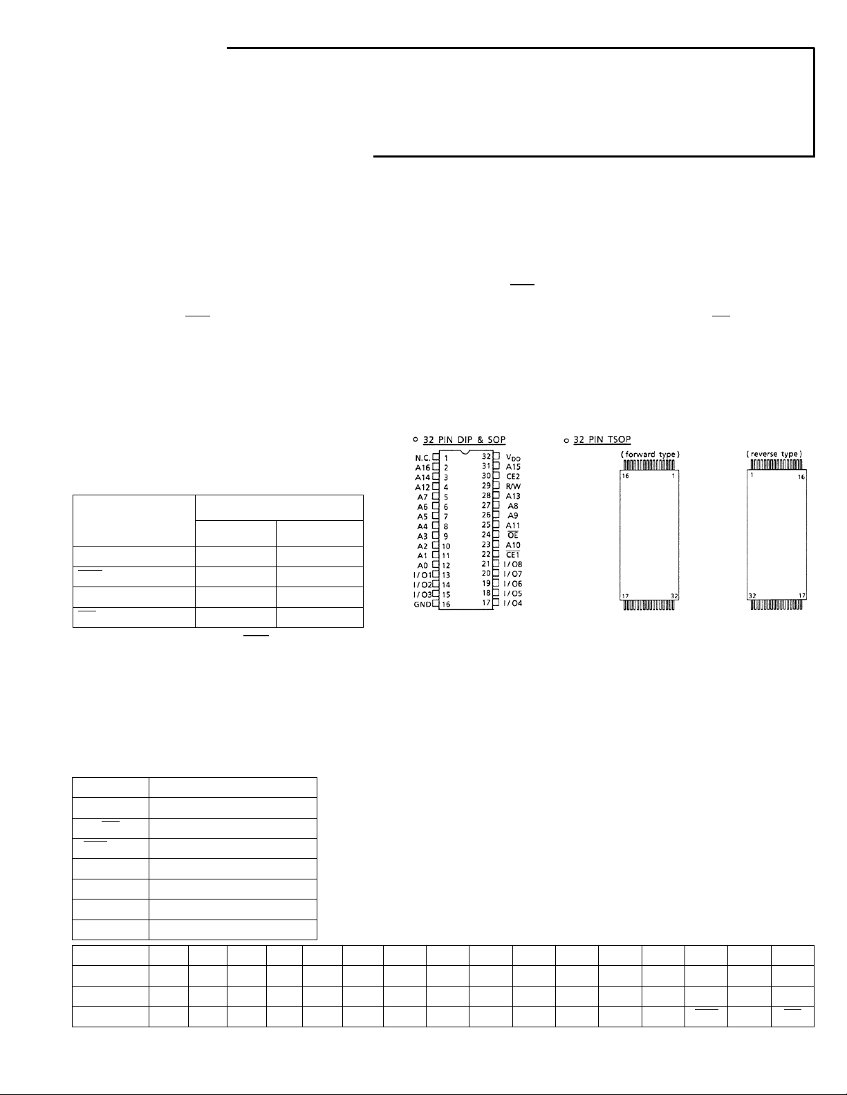
Pin Connection (Top View)
-70L -85L
Access Time
CE1 Access Time 70ns 85ns
CE2 Access Time 70ns 85ns
OE Access Time 35ns 45ns
• Power down feature: CE1
70ns 85ns
, CE2
• Data retention supply voltage: 2.0 ~ 5.5V
• Inputs and outputs directly TTL compatible
• Package TC551001BPL : DIP32-P-600
TC551001BFL : SOP32-P-525
TC551001BFTL : TSOP32-P-0820
TC551001BTRL : TSOP32-P-0820A
Pin Names
A0 ~ A16 Address Inputs
R/W Read/Write Control Input
OE Output Enable Input
CE1, CE2 Chip Enable Inputs
I/O1 ~ I/O8 Data Input/Output
V
DD
GND Ground
N.C. No Connection
PIN NO.
PIN NAME A
PIN NO.
PIN NAME A
Power (+5V)
1 2 3 4 5 6 7 8 9 10 11 12 13 14 15 16
A
A
11
17 18 19 20 21 22 23 24 25 26 27 28 29 30 31 32
9
A
3
2
A
8
13
A
A
1
0
CE2 A
R/W
I/O1
I/O2 I/O3 GND I/O4 I/O5 I/O6 I/O7 I/O8 CE1 A
TSOP Pinout
V
15
DD
NC
A
A
16
A
14
A
12
A
7
A
6
A
5
10
4
OE
TOSHIBA AMERICA ELECTRONIC COMPONENTS, INC
.
1
°
°
°
TC551001BPL/BFL/BFTL/BTRL-70L/85L Static RAM SR01020795
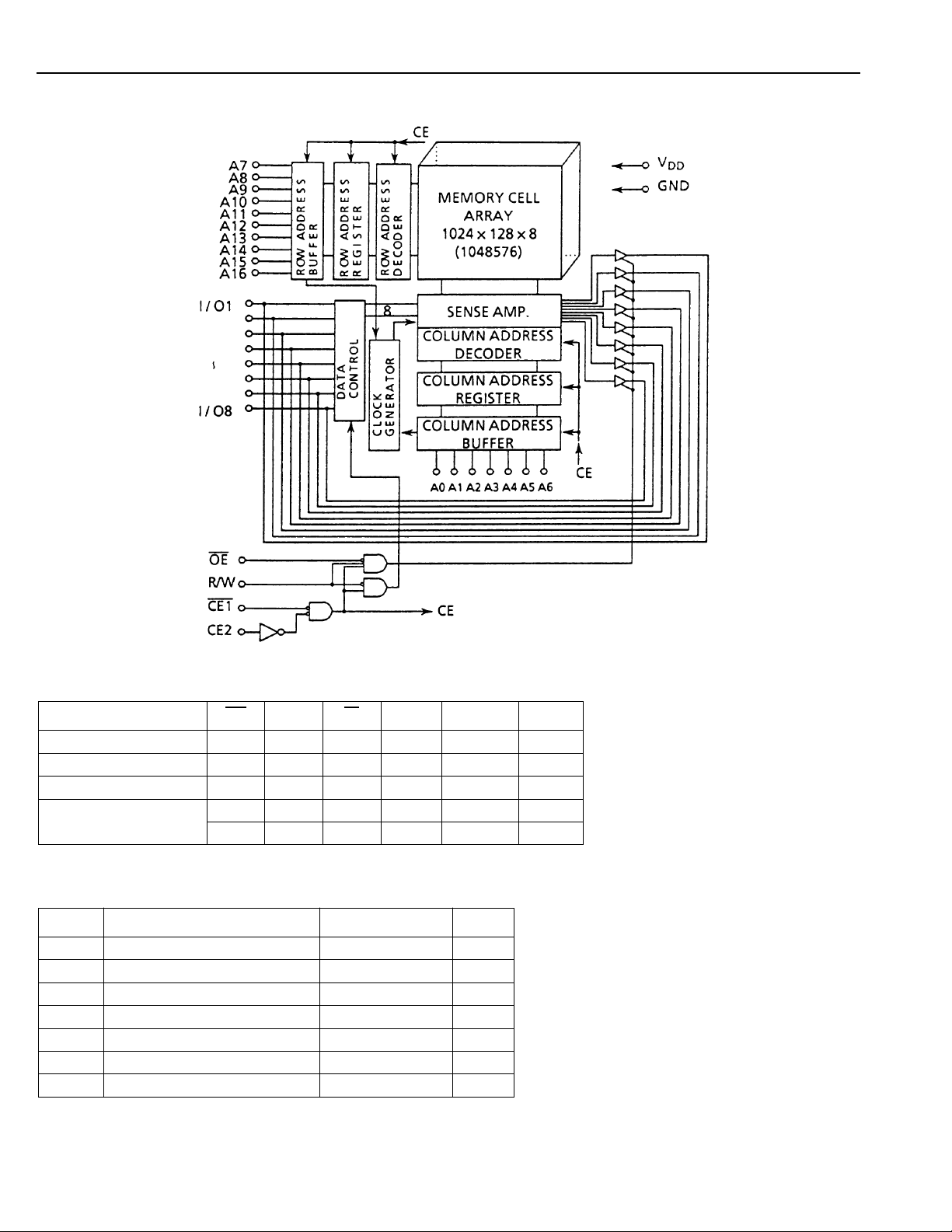
Block Diagram
Operating Mode
OPERATION MODE
Read
Write
Output Deselect
Standby
* H or L
CE1 CE2 OE R/W I/O1 ~ I/O8 POWER
L H L H D
L H * L D
L H H H High-Z I
H * * * High-Z I
*
L * * High-Z I
Maximum Ratings
SYMBOL ITEM RATING UNIT
V
V
V
P
T
SOLDER
T
STRG
T
OPR
* -3.0V at pulse width of 50ns Max
** SOP
Power Supply Voltage
DD
Input V oltage
IN
Input and Output Voltage
I/O
Power Dissipation
D
Soldering T emperature (10s)
Storage Temperature
Operating Temperature
-0.3 ~ 7.0 V
-0.3* ~ 7.0 V
-0.5 ~ V
DD
+ 0.5
1.0/0.6** W
260
-55 ~ 150
0 ~ 70
OUT
IN
V
C
C
C
I
DDO
I
DDO
DDO
DDS
DDS
2
TOSHIBA AMERICA ELECTRONIC COMPONENTS, INC
.
±
±
µ
SR01020795 Static RAM TC551001BPL/BFL/BFTL/BTRL-70L/85L
DC Recommended Operating Conditions
SYMBOL
V
V
V
V
* -3.0V at pulse width of 50ns Max.
Power Supply Voltage
DD
Input High Voltage
IH
Input Low Voltage
IL
Data Retention Supply Voltage
DH
PARAMETER MIN. TYP. MAX. UNIT
4.5 5.0 5.5
2.2 – V
-0.3* – 0.8
2.0 – 5.5
DC and Operating Characteristics (Ta = 0 ~ 70ºC, V
SYMBOL
I
Input Leakage Current
LI
I
I
I
I
DDO1
Output Leakage Current
LO
Output High Current
OH
Output Low Current
OL
Operating Current
I
DDO2
I
DDS1
Standby Current
(1)
I
DDS2
Note: (1) In standby mode with CE1 ≥ V
PARAMETER TEST CONDITION MIN. TYP. MAX. UNIT
V
IN
CE1 = V
OE
V
OH
V
OL
CE1 = V
and R/W = V
I
OUT
Other Inputs = V
CE1
CE2 = V
R/W = V
I
OUT
Other Inputs
= V
CE1 = V
CE1
CE2 = 0.2V
V
DD
- 0.2V, these specification limits are guaranteed under the condition of CE2 ≥ V
DD
= 5V ± 10%)
DD
= 0 ~ V
= V
DD
or CE2 = V
IH
V
IH,
OUT
= 2.4V
= 0.4V
and CE2 = V
IL
IH,
= 0mA
= 0.2V and
- 0.2V
DD
- 0.2V
DD
= 0mA
- 0.2V/0.2V
DD
or CE2 = V
IH
- 0.2V or
= V
DD
= 2.0V ~ 5.5V
DD
= 0 ~ V
/V
IH
IL
+ 0.3
or R/W = V
IL
DD
IH
IL
V
–
or
IL
–
–
–
1.0 µ A
1.0 µ A
-1.0 – – mA
4.0 – – mA
t
cycle
t
cycle
Min.
1 µ s – – 20
Min.
1 µ s – – 10
– – 70
– – 60
–
– 3 mA
Ta = 0 ~ 70 ° C – – 30
Ta = 25 ° C – 2 4
- 0.2V or CE2 ≤ 0.2V.
DD
mA
A
Capacitance (Ta = 25ºC, f = 1MHz)
SYMBOL
C
C
Note: This parameter is periodically sampled and is not 100% tested.
Input Capacitance
IN
Output Capacitance
OUT
PARAMETER TEST CONDITION MAX. UNIT
V
= GND
IN
V
OUT
TOSHIBA AMERICA ELECTRONIC COMPONENTS, INC
= GND
10
10
.
pF
3
TC551001BPL/BFL/BFTL/BTRL-70L/85L Static RAM SR01020795
AC Characteristics (Ta = 0 ~ 70°C, VDD = 5V±10%)
Read Cycle
TC551001BPL/BFL/BFTL/BTRL
SYMBOL PARAMETER
t
t
ACC
t
CO1
t
CO2
t
t
COE
t
OEE
t
t
ODO
t
Read Cycle Time 70 – 85 –
RC
Address Access Time – 70 – 85
CE1 Access Time – 70 – 85
CE2 Access Time – 70 – 85
Output Enable to Output in Valid – 35 – 45
OE
Chip Enable (CE1, CE2) to Output in Low-Z 10 – 10 –
Output Enable to Output in Low-Z 5 – 5 –
Chip Enable (CE1, CE2) to Output in High-Z – 25 – 30
OD
Output Enable to Output in High-Z – 25 – 30
Output Data Hold Time 10 – 10 –
OH
Write Cycle
SYMBOL PARAMETER
t
t
t
t
t
t
ODW
t
OEW
t
t
Write Cycle Time 70 – 85 –
WC
Write Pulse Width 50 – 60 –
WP
Chip Selection to End of Write 60 – 75 –
CW
Address Setup Time 0 – 0 –
AS
Write Recovery Time 0 – 0 –
WR
R/W to Output in High-Z – 25 – 30
R/W to Output in Low-Z 5 – 5 –
Data Setup Time 30 – 35 –
DS
Data Hold Time 0 – 0 –
DH
UNIT-70L -85L
MIN. MAX. MIN. MAX.
ns
TC551001BPL/BFL/BFTL/BTRL
UNIT-70L -85L
MIN. MAX. MIN. MAX.
ns
AC Test Conditions
Input Pulse Levels 2.4V/0.6V
Input Pulse Rise and Fall Time 5ns
Input Timing Measurement Reference Level 1.5V
Output Timing Measurement Reference Level 1.5V
Output Load 1 TTL Gate and CL = 100pF
4
TOSHIBA AMERICA ELECTRONIC COMPONENTS, INC
.
 Loading...