

查询TB62300FG供应商
TOSHIBA BiCD IC Silicon Monolithic
TB62300FG
Dual Full-Bridge Driver for DC Motor
The TB62300FG is a dual brushed DC motors driver IC
employing a chopper-based forward/reverse full-bridge
mechanism. It controls two brushed DC motors at high precision.
The motor supply voltage is up to 40 V and the V
voltage is 5.0 V.
Features
• A single IC can drive two brushed DC motors.
• Monolithic Bi-CMOS IC
• Low ON-resistance (R
• Selectable current control: PWM current control using the
PHASE pin or serial control
• 5-bit DA converter for specifying current value and 2-bit DA converter for determining torque
• MIXED DECAY mode enables specification of current decay rate in four steps.
• Self-oscillation chopping frequency with external resistor and capacitor
• High-speed chopping at 100 kHz or higher
• ISD, TSD, and POR (V
• Charge pump circuit (two external capacitors) for driving output
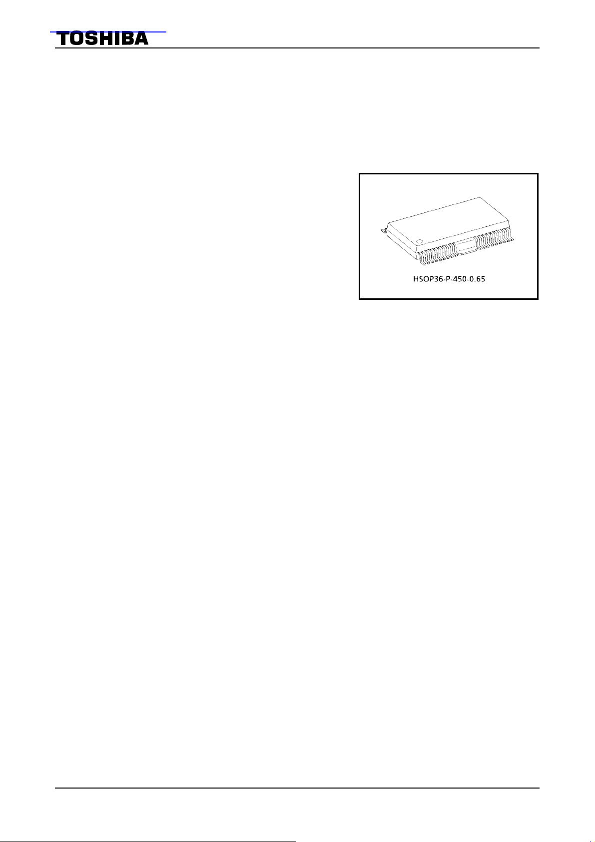
• 36-pin package: HSOP36 with heat sink
• Output voltage: 40 V (max)
• Output current: 2.5 A max (in steady-state phase) or 8 A max (pulsed output)
) = 0.3 Ω (Tj = 25°C at 2.0 A typ.)
on
) protection circuits
DD/VM
supply
DD
Weight: 0.79 g (typ.)
TB62300FG
Note: The values specified in this document are designed values, which are not guaranteed.
1
2005-04-04
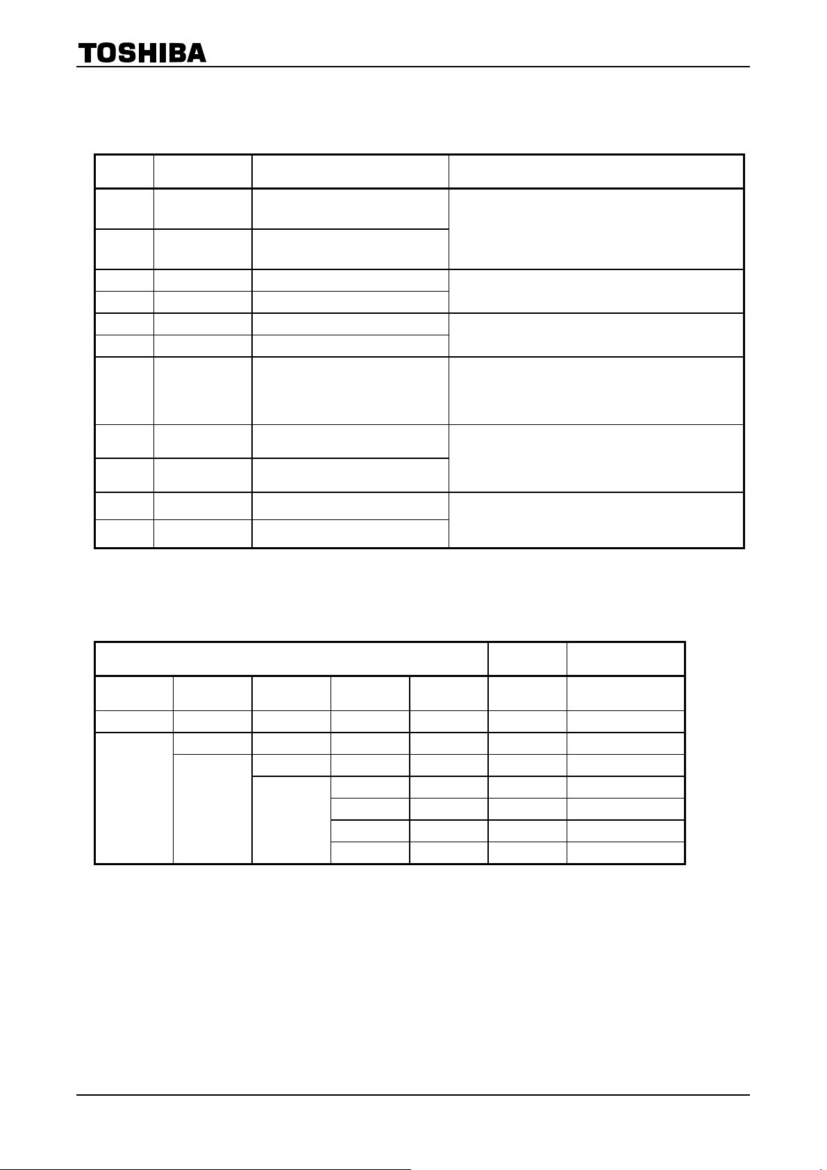
Block Diagram
TB62300FG
1.
Sleep
DATA
STROBE
Overview (for single axis)
Current control data logic circuit
Circuits used to set current value
CLK
V
ref
R
VM
Mixed decay timming,
table logic circuit
Current feedback circuit
S
16-bit shift register
Current range
controller
(2-bit D/A)
V
circuit
RS
Current value controller
(5-bit D/A)
16-bit latch
RS comparator
circuit
Chopping reference
circuit
Chopping
waveform
generator
circuit
Waveform
squaring
circuit
Output control circuit
Mixed decay control
Output pre driver
VDD
CR
MODE
PHASE
ENABLE
BRAKE
Ccp 2
Ccp 1
Charge pump
circuit
High-voltage (VM)
Logic data
Analog data
IC pin
Output circuit
(H-bridge)
Brushed DC
Motor
Out X
ISD
circuit
V
DDR/VMR
circuit
Protection circuit
TSD
circuit
2
2005-04-04

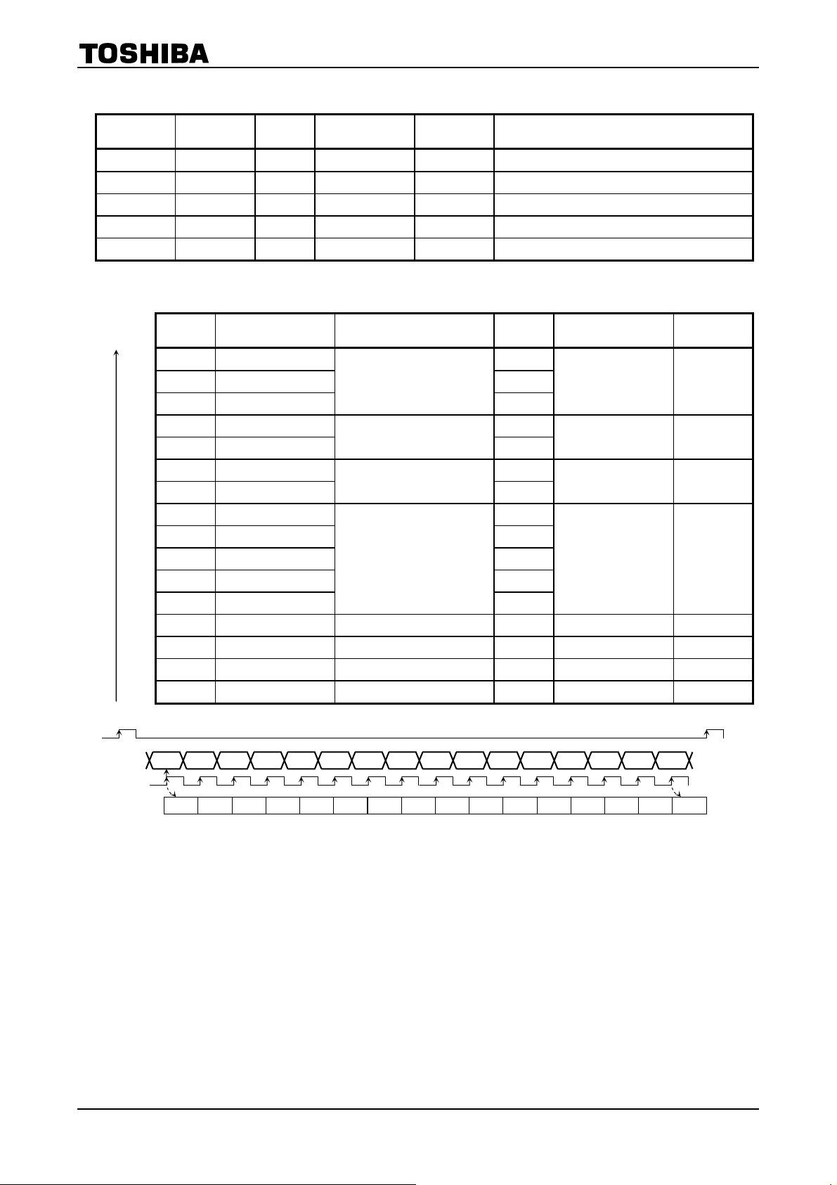
Pin Assignment
TB62300FG
R
S A
V
REF A
V
REF B
CR
V
M
Ccp 1
Ccp 2
Ccp 3
VDD
LGND
NC
TSTO
TSTI
BRAKE A
BRAKE B
1
2
3
4
5
6
7
8
9
10
11
12
13
14
36
R
35
SLEEP
34
ENABLE B
33
ENABLE A
32
PHASE B
31
PHASE A
30
DATA B
29
DATA A
28
CLK B
LGND
27
CLK A
26
STROBE B
25
STROBE A
24
MODE B
23
MODE A
S B
22
21
20
19
NC
OUT B
PGND
OUT B
−
+
OUT A
PGND
OUT A
NC
15
16
−
17
18
+
Note: When designing a ground line, make sure that all ground pins are connected to the same ground trail and
remember to take heat radiation into account.
When pins that are used to toggle between modes are controlled by a switch, pull up or down the pins to avoid
high impedance.
The IC may be destroyed due to short circuit between outputs, to supply, or to ground. Design output lines,
V
(VM) lines and ground lines with great care.
DD
When power supply pins (V
, RS, OUT, P-GND, VSS and CCP) that are exposed to high current, or logic input
M
pins are not connected correctly, excessive current or malfunction may cause the IC to break down.
3
2005-04-04
Pin Description
TB62300FG
Pin
Number
1 R
2 V
3 V
4 CR External chopping reference pin Pin used to set the chopping frequency
5 VM Supply voltage monitor pin Monitor (reference) pin for motor supply voltage
6 Ccp 1 Charge pump capacitor pin Pin for connecting a charge pump capacitor
7 Ccp 2 Charge pump capacitor pin Pin for connecting a charge pump capacitor
8 Ccp 3 Charge pump capacitor pin Pin for connecting a charge pump capacitor
9 VDD Logic power supply Logic supply current input pin
10 NC NC pin Note: Usually, leave this pin open.
11 TSTO Test pin (usually not used) Note: Usually, leave this pin open.
12 TSTI Test pin (usually not used) Note: Usually, connect this pin to LGND.
13 BRAKE A A-ch brake mode pin Forced brake mode
14 BRAKE B B-ch brake mode pin Forced brake mode
15 NC NC pin Note: Usually, leave this pin open.
16 OUT A − A-ch negative output pin A − output pin
17
18
19 OUT B + B-ch positive output pin B + output pin
20 PGND VM ground Power ground
21 OUT B − B-ch negative output pin B − output pin
22 NC NC pin Note: Usually, leave this pin open.
23 MODE A A-ch data mode switching pin Pin used to toggle between serial input and PWM control
24 MODE B B-ch data mode switching pin Pin used to toggle between serial input and PWM control
25 STROBE A A-ch latch signal input pin Data input: latched on rising edge
26 STROBE B B-ch latch signal input pin Data input: latched on rising edge
27 CLK A A-ch clock input pin Data input: referred to rising edge
28 CLK B B-ch clock input pin Data input: referred to rising edge
29 DATA A A-ch data input pin Data input:
30 DATA B B-ch data input pin Data input:
31 PHASE A A-ch phase switching pin PWM signal input pin:
32 PHASE B B-ch phase switching pin PWM signal input pin::
33 ENABLE A A-ch output forced OFF pin L: output stopped
34 ENABLE B B-ch output forced OFF pin L: output stopped
35 SLEEP Operation stopped mode Internal logic cleared and charge pump stopped
36 R
FIN1 LGND Logic ground Logic ground
FIN2 LGND Logic ground Logic ground
Symbol Function Remarks
S A
A-ch reference voltage input pin Reference power supply pin for A-axis current
REF A
B-ch reference voltage input pin Reference power supply pin for B-axis current
REF B
PGND
+
OUT A
S B
A-ch output power supply pin (current
detection pin)
VM ground Power ground
A-ch positive output pin A
B-ch output power supply pin (current
detection pin)
Reference pin for A-axis supply voltage
+ output pin
Reference pin for B-axis supply voltage
4
2005-04-04
TB62300FG
Pin Description
(Supplementary)
Pull-up/pull-down status and operation within the IC for input pins
Pin
Number
10 NC Open
11 TSTO Output pin (usually low)
12 TSTI
13 BRAKE A No pull-up or down
14 BRAKE B No pull-up or down
15 NC Open
22 NC Open
23 MODE A No pull-up or down
24 MODE B No pull-up or down
25 STROBE A No pull-up or down
26 STROBE B No pull-up or down
27 CLK A No pull-up or down
28 CLK B No pull-up or down
29 DATA A No pull-up or down
30 DATA B No pull-up or down
31 PHASE A No pull-up or down
32 PHASE B No pull-up or down
33 ENABLE A No pull-up or down
34 ENABLE B No pull-up or down
35 SLEEP Pull-down with a 50-kΩ
Symbol Internal Pull-up/down Output Operation at High Output Operation at Low
Does not affect normal operation of
the IC.
Does not affect normal operation of
the IC (with the same withstand
Input pin (no pull-up or
down)
resistor
voltage as for V
Toshiba test mode Normal operation mode
Does not affect normal operation of
the IC.
Does not affect normal operation of
the IC.
DD
).
Does not affect normal operation of
the IC.
Does not affect normal operation of
the IC.
Does not affect normal operation of
the IC.
Does not affect normal operation of
the IC.
5
2005-04-04
Truth Table (1)
Pin logic overview
Pin
Number
23 MODE A A-ch data mode switching pin
24 MODE B B-ch data mode switching pin
25 STROBE A A-ch latch signal input pin
26 STROBE B B-ch latch signal input pin
31 PHASE A A-ch phase switching pin
32 PHASE B B-ch phase switching pin
35 SLEEP Operation stopped mode
33 ENABLE A A-ch output forced OFF pin
34 ENABLE B B-ch output forced OFF pin
13 BRAKE A A-ch brake mode pin
14 BRAKE B B-ch brake mode pin
Symbol Function Logic
Truth Table (2)
TB62300FG
H : Serial signal input control
L : PWM control
Note: When PWM control is selected, serial data
bits D0 to D6 are valid while D7 to D13 are
invalid.
H : Latched on rising edge
L : Pass-through
H : Positive phase
L : Negative phase
H : Sleep released
L : Sleep state
All internal circuits, including charge pumps, are
stopped.
H : Output enabled
Output transistors turned on
L : Output disabled
Output transistors turned off
H : Brake applied
PHASE and ENABLE pins disabled
L : Brake released
Overall logic
SLEEP ENABLE
0 X X X X X Sleep mode
1
External Pins Serial Status
A/B
0 X X X X Disable mode
1
BRAKE
A/B
1 X X X Breake ON
0
MODE
A/B
0 1 X Forward
0 0 X Reverse
1 X 1 Forward
1 X 0 Reverse
PHASE
A/B
PHASE
6
2005-04-04
IC State for Each Function
Function Internal Logic Output Charge Pump OSC Recovery Time
TB62300FG
SLEEP Reset OFF OFF OFF t
ENABLE Maintained OFF Operating Operating N/A
POR Reset
ISD Reset OFF OFF OFF t
TSD Reset OFF OFF OFF t
OFF OFF OFF t
ONG
ONG
ONG
ONG
Serial Input Signals
Order of data
input
Data Bit Name Function
0 TBlank 0 0
1 TBlank 1 1
2 TBlank 2
3 Torque 0
4 Torque 1
5 Decay mode 0 1
6 Decay mode 1
7 Current 0 1
8 Current 1 1
9 Current 2 1
10 Current 3 1
11 Current 4
12 Phase Switch phase 0 Negative Disabled
13 ⎯ ⎯ ⎯ ⎯ ⎯
14 ⎯ ⎯ ⎯ ⎯ ⎯
15 ⎯ ⎯ ⎯ ⎯ ⎯
Set blanking time to prevent
false detection due to noise
Set current range
Set decay mode
Set current
= 2.0 ms (typ.)/4.0 ms (max)
= 2.0 ms (typ.)/4.0 ms (max)
= 2.0 ms (typ.)/4.0 ms (max)
= 2.0 ms (typ.)/4.0 ms (max)
Initial
Value
1
0
0
0
1
Initial State
÷ fchop ÷ 16 × 7 Enabled
1
25% Enabled
Mixed decay mode
(37.5%)
100% Disabled
When PWM is
Operating
Enabled
Strobe
Data
Clock
Register
D15 D14 D13 D12 D11 D10 D9 D8 D7 D6 D5 D4 D3 D2 D1 D0
A15 A14 A13 A12 A11 A10 A9 A8 A7 A6 A5 A4 A3 A2 A1 A0
Notes on TBlank Setting
When using PWM control and serial control simultaneously, constant-current chopping may be disabled
depending on the TBlank setting. Using constant-current chopping requires the following phase width in
Fast Decay mode:
(TBlank setting + 2/fcr) × 2
7
2005-04-04
TB62300FG
Setting Table (1): D0, D1, D2
Blanking time settings
Data Bit Name Function TBlank 2 TBlank 1 TBlank 0 Setting TBlank (typ.)
0
1
2
TBlank 0
TBlank 1
TBlank 2
Set blanking time to prevent
false detection due to noise
0 0 0 1 ÷ f
0 0 1 1 ÷ f
0 1 0 1 ÷ f
0 1 1 1 ÷ f
1 0 0 1 ÷ f
1 0 1 1 ÷ f
1 1 0 1 ÷ f
1 1 1 1
Setting Table (2): D3, D4
Torque settings
Data Bit Name Function Torque 1 Torque 0 Setting Torque (typ.)
3
4
Torque 0
Torque 1
Set current range
0 0 25%
0 1 50%
1 0 75%
1 1 100%
Setting Table (3): D5, D6
÷ f
Chop
Chop
Chop
Chop
Chop
Chop
Chop
Chop
÷ 16 × 1
÷ 16 × 2
÷ 16 × 3
÷ 16 × 4
÷ 16 × 5
÷ 16 × 6
÷ 16 × 7
÷ 16 × 8
Decay mode settings
Data Bit Name Function
5
6
Decay mode 0
Decay mode 1
Set decay mode
Torque
Mode 1
0 0 Slow decay mode
0 1 Mixed decay mode: 37.5%
1 0 Mixed decay mode: 75.0%
1 1 Fast decay mode
Torque
Mode 0
Setting Decay Mode
8
2005-04-04
TB62300FG
Setting Table (4): D7, D8, D9, D10, D11
Current settings
Data Bit Name Function Current 4 Current 3 Current 2 Current 1 Current 0 Setting Current
7
8
9
10
11
Current 0
Current 1
Current 2
Current 3
Current 4
Set current
Setting Table (5): D12
0 0 0 0 0 0%
0 0 0 0 1 3%
0 0 0 1 0 6%
0 0 0 1 1 9%
0 0 1 0 0 12%
0 0 1 0 1 16%
0 0 1 1 0 19%
0 0 1 1 1 22%
0 1 0 0 0 25%
0 1 0 0 1 29%
0 1 0 1 0 32%
0 1 0 1 1 35%
0 1 1 0 0 38%
0 1 1 0 1 41%
0 1 1 1 0 45%
0 1 1 1 1 48%
1 0 0 0 0 51%
1 0 0 0 1 54%
1 0 0 1 0 58%
1 0 0 1 1 61%
1 0 1 0 0 64%
1 0 1 0 1 67%
1 0 1 1 0 70%
1 0 1 1 1 74%
1 1 0 0 0 77%
1 1 0 0 1 80%
1 1 0 1 0 83%
1 1 0 1 1 87%
1 1 1 0 0 90%
1 1 1 0 1 93%
1 1 1 1 0 96%
1 1 1 1 1 100%
Phase settings
Data Bit Name Function Phase Setting Phase
12 Phase Switch phase
0 Negative
1 Positive
9
2005-04-04

TB62300FG
2005-04-04
1 2 3 4 5 6 ・・・・・
*16)
chop
(f
CR
PHASE
f
PWM Operation
Input range for fcr clock
Internal reset signal
1/fcr*2
*2
Example:
1/fcr
Phase Blank Time
*TBlank
*2 + 1/fcr*TBlank
1/fcr
Example: 1/fcr
Serial Blanking Time
Total Blanking Time
Output control signal
frequency.
chop
is 16 times the f
cr
・PHASE is an external signal.
・The internal reset signal resets the internal clocks and counters.
・Phase Blank Time is time between either edge of the external PHASE signal and the leading edge of serial blanking time.
Notes: ・f
The output H bridge is driven by an external PHASE signal.
Description
It, however, also uses the fcr signal, generated with external CR, to generate blanking time and Mixed Decay time. The above logic is configured to handle the two
signals, PHASE and fcr, which are asynchronous to each other. The logic generates internal reset signal edges from external PHASE edges, resulting in the width
equal to two fcr cycles.
The fcr-based counter assumes the first fcr falling edge following the PHASE edge as the first count. The maximum phase difference between the PHASE and fcr
signals is, therefore, one fcr cycle. The serial blanking time starts at the second count based on the fcr clock (The first three samples of serial blanking time signal must be 000).
The last stage output is switched by the edge of the external PHASE signal. That means there is an interval of two fcr cycles before the set blanking time starts.
To cover the interval, the logic generates the time between the PHASE signal edge and blanking time start as phase blank time, during which comparison is masked
difference between PHASE and fcr (up to two fcr cycles).
off in the same way as in blanking time.
Consequently, the blanking time as viewed from outside the IC is within the range from one fcr cycle (TBlank (000)) to eight fcr cycles (TBlank (111)) + I phase
10

TB62300FG
Absolute Maximum Ratings
Characteristics Symbol Test Condition Rating Unit
Logic supply voltage VDD ⎯ −0.4 to 7.0 V
Maximum output voltage VM ⎯ 40 V
Peak output current
(Note: preliminary specification)
Continuous output current I
Logic input voltage VIN ⎯ −0.5 to VDD V
Current detection pin voltage VRS ⎯ V
Power dissipation PD
Operating temperature T
Storage temperature T
Junction temperature Tj ⎯ 150 °C
Note: When T
= 45°C, Tj = 150°C and θja = 32°C
opr
(T
= 25°C)
opr
I
OUT (Peak)tW
OUT (Cont)
⎯ −40 to 85 °C
opr
⎯ −55 to 150 °C
stg
≤ 500 ns 8.0 A
⎯ 2.5 A
± 4.5 V V
M
IC alone 1.4 W
When mounted on a board
(Note)
3.2 W
Recommended Operating Conditions
Characteristics Symbol Test Condition Min Typ. Max Unit
(T
= 0 to 85°C)
opr
Supply voltage (Note 1) VDD ⎯ 4.5 5.0 5.5 V
Output voltage (Note 1) VM VDD = 5.0 V 18.0 24.0 33.0 V
I
Output current
(Note: preliminary specification)
Logic input voltage range VIN ⎯ 0 ⎯ VDDV
Clock frequency f
Chopping frequency f
V
reference voltage V
ref
Current detection pin voltage VRS VDD = 5.0 V 0 ±1.0 ±1.5 V
Junction temperature Tj ⎯ ⎯ ⎯ 120 °C
Oscillator capacitor C
Oscillator resistor R
Charge pump capacitor A C
Charge pump capacitor B C
Input rise and fall rate (Note 2) tri/tfi ⎯ ⎯ 0.1 5.0 µs
OUT (Peak)VM
I
OUT (Cont)VM
VDD = 5.0 V 1.0 25.0 MHz
CLK
VDD = 5.0 V 20 30 150 kHz
chop
VM = 24.0 V, T
ref
⎯ ⎯ 270 ⎯ pF
OSC
⎯ ⎯ 3.9 ⎯ kΩ
OSC
⎯ ⎯ 0.22 ⎯ µF
CPA
⎯ ⎯ 0.022 ⎯ µF
CPB
= 33.0 V, tw ≤ 500 ns ⎯ 6.4 7.2 A
= 33.0 V ⎯ 1.5 1.8 A
= 100% 2.0 3.0 V
ORQUE
DD
Note 1: Do not reduce VDD to 0 V (ground) while VM voltage is applied. Such an attempt may damage the IC
because there is a current path from the V
not applied. Leaving V
open (Hi-Z) is less likely to damage the IC, although it is not recommended.
DD
pin to VDD pin and the internal logic is undefined when VDD is
M
Note 2: The circuit configuration of this IC cannot handle extremely slow data input (on pins BREAK A, BREAK B,
SLEEP, ENABLE A, ENABLE B, PHASE A, PHASE B, DATA A, DATA B, CLK A, CLK B, STROBE A,
STROBE B, MODE A, and MODE B). Applying a slow signal having a period longer than 5 µs may cause
the IC to oscillate.
(1) Calculating the current
= 1/3 × V
I
OUT
where 1/3 is the V
(V) × (Torque (%) ÷ RRS (Ω) ) × Current (%)
ref
(GAIN):V
ref
attenuation ratio.
ref
(2) Calculating the oscillation frequency
= 1/(KA) × (C × R + KB × C)) × [Hz]
f
CR
KA = 0.523, KB = 600, f
= fCR/16 [Hz]
chop
[Example] When C
= 270 pF and R
OSC
= 3.9 kΩ: fCR = 1.57 MHz and f
OSC
= 1.57/16 = 98.4 kHz
chop
V
11
2005-04-04

Electrical Characteristics 1
TB62300FG
DC Characteristics
Characteristics Symbol
Input voltage
Input current
Current consumed by logic power
supply
VM current consumption
(unless otherwise specified, VM = 24 V, VDD = 5.0 V, T
High V
Low V
I
IH1
I
IL1
I
IH2
I
IL2
I
DD1
I
DD2
IM1
IM2
Test
Circuit
IH
DC
IL
DC
DC
DC
Test Condition Min Typ. Max Unit
CLK, STROBE, DATA, MODE,
2.0 ⎯
PHASE, ENABLE and PHASE
pins
CLK, STROBE, DATA, MODE,
⎯ ⎯ 0.8
⎯ ⎯ 1.0
PHASE, ENABLE and PHASE
pins
⎯ ⎯
⎯ ⎯
SLEEP pin
⎯ ⎯
VDD = 5.0 V, fcr stopped ⎯ 3.0 4.5
In SLEEP mode
Output open, f
logic operating, V
V
= 24 V, all output stages
M
CLK
DD
= 1 kHz,
= 5 V,
stopped, charge pump charged
Output open, f
CLK
= 4 kHz,
internal logic operating
(100-kHz chopping), output
stages operating without load,
charge pump charged
0.3 1.0
⎯ 4.3 7.0
⎯ 20.0 28.0
= 25℃)
opr
⎯
1.0
200.0
1.0
V
µA
µA
mA
mA
Output standby current Upper I
Output bias current Upper I
Output leakage current Lower I
High V
Comparator reference
voltage ratio
Mid
High
Mid
Low
Low
V
V
V
I
M3
OH
OB
OL
RS (H)
RS (MH)
RS (ML)
RS (L)
In SLEEP mode ⎯ 0.5 1.0
VRS = VM = 24 V, V
ENABLE
DATA
VRS = VM = 24 V, V
DC
ENABLE
DATA
V
= Low,
= All low
= Low,
= All low
= VM = Ccp A = V
RS
= 24 V, SLEEP= Low
V
= 3.0 V, V
ref
TORQUE
V
= 3.0 V, V
ref
TORQUE
= 11 = 100% set
= 10 = 75% set
DC
V
= 3.0 V, V
ref
TORQUE
V
= 3.0 V, V
ref
TORQUE
= 01 = 50% set
= 00 = 25% set
= 0 V,
out
= 24 V,
out
out
(gain) = 1/3.0
ref
(gain) = 1/3.0
ref
(gain) = 1/3.0
ref
(gain) = 1/3.0
ref
−400 ⎯ ⎯
−200 ⎯ ⎯
⎯ ⎯ 1.0
µA
⎯ 100 ⎯
73 75 77
%
48 50 52
23 25 27
12
2005-04-04

TB62300FG
Electrical Characteristics 2
DC Characteristics
Characteristics Symbol
Output current interchannel error ∆I
Output current setting error ∆I
RS pin current I
Output transistor drain-source
ON-resistance
V
input voltage V
REF
unless otherwise specified,
(
OUT1
OUT2
RS
RON1
RON1
RON2
RON2
ref
Test
Circuit
DC
DC I
DC µA
DC
DC
VM = 24 V, VDD = 5.0 V, T
Test Condition Min Typ. Max Unit
Error in output current between
channels (I
= 1.5 A −5.0 ⎯ 5.0 %
OUT
= 1.5 A, VDD = 5.0 V,
I
OUT
T
= 25 °C, forward direction
j
= 1.5 A, VDD = 5.0 V,
I
OUT
T
= 25 °C, reverse direction
j
= 1.5 A, VDD = 5.0 V,
I
OUT
T
= 105 °C, forward direction
j
= 1.5 A, VDD = 5.0 V,
I
OUT
T
= 105 °C, reverse direction
j
= 24 V, VDD = 5.0 V,
V
M
ENABLE, output operation
OUT
= 1.5 A)
−5.0 ⎯ 5.0
⎯ 0.3 0.4
⎯ 0.3 0.4
⎯ 0.4 0.55
⎯ 0.4 0.55
2.0
= 25℃)
opr
⎯ V
DD
%
Ω
V
= 3.0 V,
V
ref
V
input current I
REF
V
attenuation ratio
REF
TSD operating temperature (Note 1) TjTSD DC VDD = 5 V, VM = 24 V 130 ⎯ 170 °C
Overcurrent protection circuit
operating current
Output OFF mode supply voltage
ref
V
ref
(GAIN)
ISD DC V
Vpor
(V
)
DD
Vpor
(V
)
M
DC
DC
DC V
DC V
V
= 24 V, VDD = 5.0 V,
M
SLEEP
= 3.0 V,
V
ref
V
= 24 V, VDD = 5.0 V,
M
SLEEP
= 5 V, VM = 24 V ⎯ 6.0 ⎯ A
DD
= 24 V ⎯ 3.0 ⎯
M
= 5 V ⎯ 15.0 ⎯
DD
⎯ ⎯ 100 µA
1/2.82 1/3 1/3.18 ⎯
V
Note 1: Thermal shutdown (TSD) circuit
When the IC junction temperature reaches the specified value and the TSD circuit is activated, the internal
reset circuit turns output off. The TSD activation temperature can be set within the range from 130°C (min)
to 170°C (max). Once the TSD circuit is activated, output is stopped until a pulse (L to H to L) is
subsequently applied to the SLEEP pin. The charge pump is halted while the TSD circuit is active.
The TSD circuit does not include hysteresis. Applying a pulse (L to H to L) to the SLEEP pin deactivates the
circuit.
Note 2: Overcurrent protection circuit (ISD)
This circuit is activated when a current pulse exceeding the specified output value is applied for a period of
1/2f
CHOP
(min) to f
CHOP
(max).
The circuit activates the internal reset circuit to turn output off.
Once it is activated, output is stopped until a pulse (L to H to L) is subsequently applied to the SLEEP pin.
While the ISD circuit is active, the IC is placed in SLEEP mode with the charge pump halted.
13
2005-04-04

TB62300FG
AC Characteristics
(T
= 25°C, VM = 24 V, VDD = 5 V
opr
Characteristics Symbol
Clock frequency f
Minimum clock pulse width
Minimum STROBE pulse width
Minimum SLEEP pulse width t
Phase difference between PHASE
signal and fcr
Blanking time for preventing false
detection
Data setup time
Data hold time
STROBE setup time (relative to CLK)
STROBE hold time (relative to CLK)
CLK
tw (t
CLK
t
wp
t
wn
t
WSTROBE
t
STROBE (H)
t
STROBE (L)
WSTROBE
tp AC
t
BLNIK
t
sSIN-CLK
t
sST-CLK
t
hSIN-CLK
t
hST-CLK
t
sSSB-CLK
t
hSB-CLK
Test
Circuit
with load of
Test Condition Min Typ. Max Unit
6.8 mH/5.7 Ω)
⎯ 1.0 ⎯ 25.0 MHz
)
AC
AC
AC t
⎯ ⎯ 1/f
(Note 1) ⎯ 300 ⎯ ns
40.0 ⎯ ⎯
20.0 ⎯ ⎯
20.0
⎯ ⎯
40.0 ⎯ ⎯
20.0 ⎯ ⎯
20.0
ONG
⎯ ⎯
⎯ ⎯ ns
CR
20.0 ⎯ ⎯
AC
20.0 ⎯ ⎯
20.0
⎯ ⎯
AC
AC
AC
20.0
⎯ ⎯
20.0 ⎯ ⎯
20.0 ⎯ ⎯
ns
ns
ns
ns
ns
ns
⎯ 40.0 100
⎯ 40.0 100
⎯ 100 200
⎯ 580 1000
AC
⎯ 100 200
C
osc
= 270 pF, R
= 3.9 kΩ 1.1 1.3 1.5 MHz
osc
⎯ 350 700
⎯ 1000 2000
⎯ 350 700
20.0 ⎯ 150.0 kHz
When f
= 480 kHz ⎯ 30.0 ⎯ kHz
CR
AC ⎯ 2.0 4.0 ms
Output transistor switching time
CR reference signal oscillation
frequency
f
chop (min)
Chopping frequency
f
chop (typ.)
f
chop (max)
Oscillation frequency f
Charge pump rise time t
t
t
t
pLH
t
pHL
t
pLZ
t
pHZ
t
pZL
t
pZH
f
CR
chop
ONG
f
f
Note 1: The blanking time is internally fixed but it can be elongated by applying a serial blanking time signal.
ns
14
2005-04-04

TB62300FG
Test Circuit
R
osc
5 V
C
5 V
0 V
5 V
0 V
5 V
0 V
5 V
0 V
5 V
0 V
5 V
0 V
5 V
0 V
5 V
0 V
5 V
0 V
5 V
0 V
5 V
0 V
5 V
0 V
5 V
0 V
5 V
0 V
5 V
0 V
osc
LGND
(DC)
= 3.6 kΩ
= 560 pF
I
DD1IDD2
A
A
A
A
A
LGND
A
A
A
A
A
A
A
A
A
A
A
V
DD
CR
STROBE A
CLK A
DATA A
STROBE B
CLK B
DATA B
SLEEP
LGND
(F
PHASE A
PHASE B
ENABLE A
ENABLE B
MODE A
MODE B
BRAKE A
BRAKE B
A
V
ref
V
B
ref
V
M
R
RS A
A
A
)
IN
B
B
R
RS B
P-GND
Ccp 3Ccp 2Ccp 1
A
A
I
RS
I
ref
A
I
ref
A
IM1, IM2, I
V
I
OUT1, 2
DC Motor
PGND
M3
V
RS
M
M
R
RS A
DC Motor
R
RS B
SGND
ref
V
ref
V
0.22
0.22
3 V
LGND
3 V
LGND
Ω
Ω
100 µF
I
I
I
OL
OH
OB
A
1 µF
1 µF
24 V
Ccp 2
0.022
µF
LGND
Ccp 1
V
0.22
µF
15
2005-04-04

TB62300FG
µ
Test Circuit
f
, tw (t
CLK
t
wSTROBE
t
sSIN-CLK
f
,
chop
fosc
R
osc
5 V
C
5 V
0 V
5 V
0 V
5 V
0 V
5 V
0 V
5 V
0 V
5 V
0 V
5 V
0 V
5 V
0 V
5 V
0 V
5 V
0 V
5 V
0 V
5 V
0 V
5 V
0 V
5 V
0 V
5 V
0 V
osc
SGND
(AC)
), twp, twn,
CLK
, t
STROBE (H)
, t
sST-CLK
= 3.6 kΩ
= 560 pF
, t
hSIN-CLK
, t
STROBE (L)
LGND
A
A
A
A
A
A
A
A
, t
hST-CLK
,
V
DD
CR
STROBE A
CLK A
DATA A
STROBE B
CLK B
DATA B
SLEEP
V
SS
(F
PHASE A
PHASE B
ENABLE A
ENABLE B
MODE A
MODE B
BRAKE A
BRAKE B
I
I
A
RS
ref
A
V
I
OUT1, 2
DC Motor
V
RS
M
M
R
RS A
DC Motor
R
RS B
PGND
ref
3 V
V
LGND
ref
3 V
V
LGND
I
OL
I
OH
I
OB
Ω
Ω
F
100
A
1.0
1.0
1 µF
1 µF
t
BLNIK
24 V
A
V
ref
V
B
ref
V
M
R
RS A
A
)
IN
Ccp 3Ccp 2Ccp 1
A
B
B
R
RS B
P-GND PGND
Ccp 1
V
0.22
µF
Ccp 2
0.022
t
ONG
µF
16
2005-04-04

AC Test Waveforms
TB62300FG
DATA
CLOCK
STROBE
SLEEP
PHASE
Out A
PHASE
ENABLE
DATA 15 50% DATA 0 DATA 1
tw (t
CLK)
twntwn t
t
sDATA
t
hDATA
sSTROBE
50%
t
50%
t
wSTROBE
50%
t
pLH
50%
dCLOOK
50%
t
wSLEEP
t
pHL
Out A
t
pZH
t
pHZ
t
pZL
t
pLZ
17
2005-04-04

TB62300FG
Waveform in Mixed Decay Mode
(Current Waveform)
f
f
chop
Internal
CR CLK
signal
I
OUT
Set current
value
25%
Mixed
Decay
Mode
NF
MDT (Mixed Decay Timming) point
Output Transistor Operating Mode
V
M
chop
Set current value
RNF
V
V
M
NF
M
R
U1
ON
L1
OFF
RS
RS pin
U2
(Note)
Load
PGND
Charge mode Slow mode Fast mode
OFF
L2
ON
U1
OFF
L1
R
Output Transistor Operation Functions
CLK U1 U2 L1 L2
Charge ON OFF OFF ON
Slow OFF OFF ON ON
Fast OFF ON ON OFF
RS
RS pin RS pin
(Note)
Load
U2
OFF
L2
ON
PGND
U1
OFF
L1
ONON
(Note)
Load
RRS
U2
ON
L2
OFF
PGND
Note: The above table is an example where current flows in the direction of the arrows in the above figures.
When the current flows in the opposite direction of the arrows, see the table below.
CLK U1 U2 L1 L2
Charge OFF ON ON OFF
Slow OFF OFF ON ON
Fast ON OFF OFF ON
18
2005-04-04

TB62300FG
Power Supply Sequence
V
DD
V
M
Internal reset
V
V
V
GND
VM
V
V
GND
Non-reset
Reset
DD (max)
DD (min)
DDR
M (min)
MR
(Recommended)
SLEEP input
(Note1)
Note 1: If V
internally reset.
This is a protective measure against malfunction. Likewise, if V
regulation voltage is applied to V
To avoid malfunction, when turning on V
recommended.
It takes time for the output control charge pump circuit to stabilize. Wait up to t
before driving a motor.
Note 2: When the V
such a case, the charge pump circuit cannot operate properly because of insufficient voltage. The IC should
be held in SLEEP mode until V
Note 3: Since V
At that time, a current of several mA flows due to a current path between V
When the output voltage is high, make sure that the specified voltage is applied to V
H
L
Takes up to t
Non-operable area
drops to the level of the V
DD
value is between 3.3 to 5.5 V, the internal reset is released, thus output may be active. In
M
= 0 V and VM = voltage within the rating are applied, output is turned off by internal reset.
DD
or below while the specified voltage is applied to the VM pin, the IC is
DDR
, the IC is internally reset as a protective measure against malfunction.
DD
reaches 13 V or more.
M
or VDD, applying a signal to the SLEEP pin at the above timing is
M
until operable
ONG
drops to the level of VMR or below while
M
time after power on
ONG
and VDD.
M
DD
.
19
2005-04-04

TB62300FG
PD – Ta
Transient thermal resistance
(1) HSOP36 R
(2) When mounted on a board (140 mm × 70 mm × 1.6 mm: 38°C/W: typ.)
(Package power dissipation)
3.5
3
2.5
(W)
D
2
1.5
(1)
1
Power dissipation P
0.5
0
0
25 50 75 100 125 150
without a board (96°C/W)
th (j-a)
P
– Ta
D
(2)
Ambient temperature Ta (°C)
Note: R
th (j-a)
: 8.5°C/W
20
2005-04-04

TB62300FG
Relationship between VM and VH
Note: VDD = 5 V
Ccp 1 = 0.22 µF, Ccp 2 = 0.022 µF, f
(Care must be taken about the temperature charges of charge pump capacitor.)
50
V
40
30
voltage Charge up voltage VM voltage
H
Apply SLEEP signal.
(charge pump voltage)
= 150 kHz
chop
V
– VH (& Vcharge UP)
M
Charge pump
output voltage
voltage, charge up voltage (V)
20
H
V
10
VMR
Recommended operation area
Usable area
0
0
2 3 10 20 30 404 5 6 7 8 9 11 12 13 14 15 16 17 18 21 22 23 24 25 2619 27 28 29 31 32 33 34 35 36 37 38 39 1
Supply voltage VM (V)
VM voltage
Maximum rating
Charge pump voltage VH = VDD + VM (= Ccp A) (V)
(Maximum rating is V
(7 V) + VM (40 V))
DD
21
2005-04-04

Operation of Charge Pump Circuit
VDD = 5 V
RS
TB62300FG
R
RS
= 24 V
V
M
V
M
V
H
Ccp A
7
Comparator
and
Controller
Output
Output
H switch
i2
Di2
r2
V
Di3
Di1
(1)
z
T
T
r1
i1
(2)
Ccp B
Ccp 2
0.022
(2)
R
1
Ccp C
µF
Ccp 1
0.22
µF
VH = VM + VDD = charge pump voltage
i1 = charge pump current
i2 = gate block power dissipation
• Initial charging
(1) When RESET is released, T
(2) After T
is turned off and Tr2 is turned on, and Ccp 1 is charged from Ccp 2 via Di2.
r1
(3) When the voltage difference between V
reaches V
or higher, operation halts (in the steady-state phase).
DD
is turned on and Tr2 turned off. Ccp 2 is charged from VM via Di1.
r1
and VH (Ccp A pin voltage = charge pump voltage)
M
• Actual operation
(4) The charge of Ccp 1 charge is used at f
switching and the potential of VH drops.
chop
(5) The circuit is charged up by the operations of (1) and (2) above.
Output switching
Initial charging Steady-state phase
V
H
V
M
(1)
(2) (3)
(4)
t
(5)
(4)
(5)
22
2005-04-04

Charge Pump Rise Time
TB62300FG
V
M
STANDBY
+ VM
V
DD
+ (VDD × 90%)
V
M
5 V
0 V
t
: Time taken for capacitor Ccp 2 (charging capacitor) to fill up Ccp 1 (storing capacitor) to VM + VDD
ONG
after a reset is released.
The internal circuits cannot drive the gates correctly until the voltage of Ccp 1 reaches V
Be sure to wait for t
Basically, the larger the Ccp 1 capacitance is, the smaller the voltage fluctuation is, though the
initial charge up time is longer.
The smaller the Ccp 1 capacitance is, the shorter the initial charge-up time is, but the voltage
fluctuation is larger.
Depending on the combination of capacitors (especially with small capacitance), voltage may not be
sufficiently boosted. When the voltage does not increase sufficiently, R
lower than the reference value, which raises the temperature.
Thus, use the capacitors under the capacitor combination conditions (Ccp 1 = 0.22 µF, Ccp 2 = 0.022
µF) recommended by Toshiba.
Ccp 1 voltage
50%
t
ONG
+ VDD.
M
or longer before driving the motors.
ONG
of output DMOS becomes
ON
23
2005-04-04

External Capacitor for Charge Pump
TB62300FG
When driving a motor while VDD = 5 V, f
= 150 kHz, L = 10 mH under the conditions of V
chop
= 27 V and
M
2.0 A, the logical values for Ccp 1 and Ccp 2 are as shown in the graph below:
Ccp 1 – Ccp 2
0.05
0.045
0.04
0.035
0.03
0.025
0.02
0.015
Ccp 2 capacitance (µF)
0.01
0.005
0
0
0.05 0.1 0.15 0.2 0.25 0.35 0.4
Applicable range
Recommended
0.3
Ccp 1 capacitance (µF)
value
0.45 0.5
Choose Ccp 1 and Ccp 2 to be combined from the above applicable range. We recommend Ccp 1:Ccp 2 at
10:1 or more. (If our recommended values (Ccp = 0.22 µF, C cp 2 = 0.022 µF) are used, the drive conditions in
the specification sheet are satisfied. (There is no capacitor temperature characteristic as a condition.)
When setting the constants, make sure that the charge pump voltage is not below the specified value and
set the constants with a margin (the larger Ccp 1 and Ccp 2, the more the margin).
Some capacitors exhibit a large change in capacitance according to the temperature. Make sure the above
capacitance is obtained under the IC ambient temperature.
24
2005-04-04

Recommended Application Circuit
µ
µ
The values of external constants are example recommended values. For values under different input
conditions, see the above-mentioned recommended operating conditions.
(The following shows an example when fcho = 501 Hz (CR frequency = 800 kHz and constant-current
limiter = 2.27 A) with serial signals placed in initial status.)
V
F
10
SGND
5 V
0 V
5 V
0 V
5 V
0 V
5 V
0 V
5 V
0 V
5 V
0 V
5 V
0 V
5 V
0 V
5 V
0 V
5 V
0 V
5 V
0 V
5 V
0 V
5 V
0 V
5 V
0 V
5 V
0 V
5 V
R
osc
C
osc
= 3.6 kΩ
= 560 pF
LGND
DD
CR
STROBE A
CLK A
DATA A
STROBE B
CLK B
DATA B
SLEEP
LGND
(F
PHASE A
PHASE B
ENABLE A
ENABLE B
MODE A
MODE B
BRAKE A
BRAKE B
)
IN
Ccp 3Ccp 2Ccp 1
V
ref
V
ref
V
R
RS A
R
RS B
P-GND
TB62300FG
A
B
M
A
A
M DC Motor
B
B
M
PGND
R
RS A
DC Motor
R
RS B
LGND
ref
V
0.11
0.11
3 V
LGND
Ω
Ω
100 µF
F
1
24 V
Ccp 2
0.022
µF
LGND
Ccp 1
0.22
µF
Note: It is recommended to add bypass capacitors as required.
Make sure that all gound pins are connected to the same ground rail.
STROBE, CLK, and DATA must be tied to LGND if serial input is not used for settings or motor control.
Because there may be short circuits between outputs, to supply, or to ground, be careful when designing
output lines, V
(VM) lines, and ground lines.
DD
25
2005-04-04

TB62300FG
Connection Diagram
3 V
3 V 10 µF
10 µF
3.9 k
24 V
100 µF
5 V
10 µF
(when external forced PWM mode is used)
0.5 Ω
Ω
270 pF
0.022
0.22 µF
5 V
NC
µF
1
2
3
4
5
6
7
8
9
10
R
S A
V
REF A
V
REF B
CR
V
M
Ccp 1
Ccp 2
Ccp 3
V
DD
LGND
TEST A
R
SLEEP
ENABLE B
ENABLE A
PHASE B
PHASE A
DATA B
DATA A
CLK B
LGND
CLK A
S B
0.5 Ω
36
35
34
33
32
31
30
29
28
27
NC
PGND
26
25
24
23
22
21
−
20
19
M M
NC
TEST B
11
TEST C
12
13
BRAKE A
BRAKE B
14
15
NC
16
OUT A
17
PGND
18
OUT A
−
+
: Signal from central unit
STROBE B
STROBE A
MODE B
MODE A
OUT B
OUT B +
26
2005-04-04

Package Dimensions
HSOP36-P-450-0.65
TB62300FG
Unit: mm
Weight: 0.79 g (typ.)
27
2005-04-04

TB62300FG
RESTRICTIONS ON PRODUCT USE
• The information contained herein is subject to change without notice.
• The information contained herein is presented only as a guide for the applications of our products. No
responsibility is assumed by TOSHIBA for any infringements of patents or other rights of the third parties which
may result from its use. No license is granted by implication or otherwise under any patent or patent rights of
TOSHIBA or others.
• TOSHIBA is continually working to improve the quality and reliability of its products. Nevertheless, semiconductor
devices in general can malfunction or fail due to their inherent electrical sensitivity and vulnerability to physical
stress. It is the responsibility of the buyer, when utilizing TOSHIBA products, to comply with the standards of
safety in making a safe design for the entire system, and to avoid situations in which a malfunction or failure of
such TOSHIBA products could cause loss of human life, bodily injury or damage to property.
In developing your designs, please ensure that TOSHIBA products are used within specified operating ranges as
set forth in the most recent TOSHIBA products specifications. Also, please keep in mind the precautions and
conditions set forth in the “Handling Guide for Semiconductor Devices,” or “TOSHIBA Semiconductor Reliability
Handbook” etc..
• The TOSHIBA products listed in this document are intended for usage in general electronics applications
(computer, personal equipment, office equipment, measuring equipment, industrial robotics, domestic appliances,
etc.). These TOSHIBA products are neither intended nor warranted for usage in equipment that requires
extraordinarily high quality and/or reliability or a malfunction or failure of which may cause loss of human life or
bodily injury (“Unintended Usage”). Unintended Usage include atomic energy control instruments, airplane or
spaceship instruments, transportation instruments, traffic signal instruments, combustion control instruments,
medical instruments, all types of safety devices, etc.. Unintended Usage of TOSHIBA products listed in this
document shall be made at the customer’s own risk.
030619EBA
• The products described in this document are subject to the foreign exchange and foreign trade laws.
• TOSHIBA products should not be embedded to the downstream products which are prohibited to be produced
and sold, under any law and regulations.
28
2005-04-04
 Loading...