

y
查询TB62209F供应商
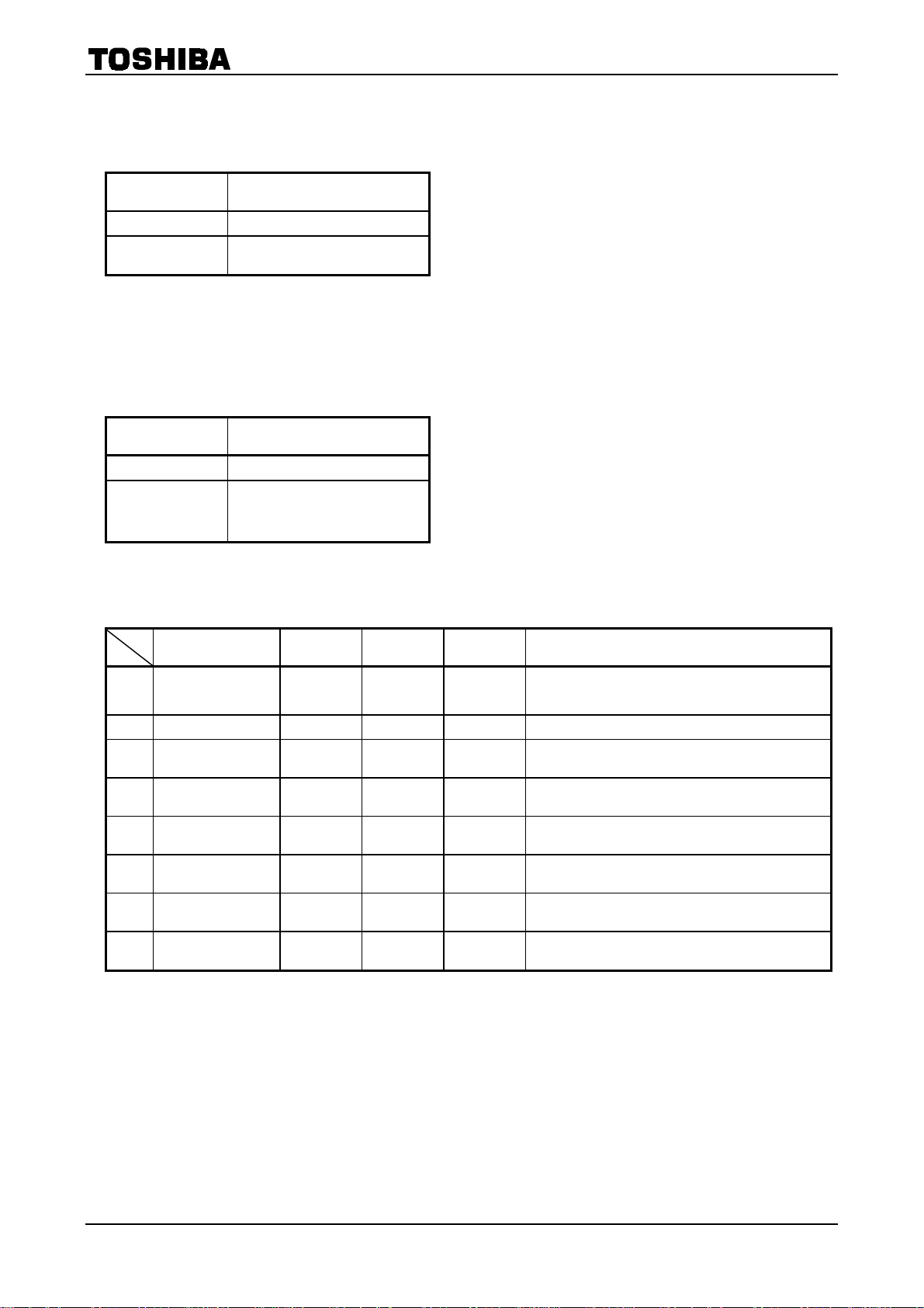
TB62209F
TOSHIBA BiCD Processor IC Silicon Monolithic
Preliminar
T B 6 2 2 0 9 F
Stepping Motor Driver IC Using PWM Chopper Type
The TB62209F is a stepping motor driver driven by chopper
micro-step pseudo sine wave.
The TB62209F integrates a decoder for CLK input in micro
steps as a system to facilitate driving a two-phase stepping motor
using micro-step pseudo sine waves. Micro-step pseudo sine
waves are optimal for driving stepping motors with low-torque
ripples and at low oscillation. Thus, the TB62209F can easily
drive stepping motors with low-torque ripples and at high
efficiency.
Also, TB62209F consists output steps by DMOS (Power MOS
FET), and that makes possible to control the output power
dissipation much lower than ordinary IC with bipolar transistor output.
The IC supports Mixed Decay mode for switching the attenuation ratio at chopping. The switching time for the
attenuation ratio can be switched in four stages according to the load.
Features
Weight: g (typ.)
• Bipolar stepping motor can be controlled by a single driver IC
• Monolithic BiCD IC
• Low ON-resistance of R
• Built-in decoder and 4-bit DA converters for micro steps
• Built-in ISD, TSD, V
• Built-in charge pump circuit (two external capacitors)
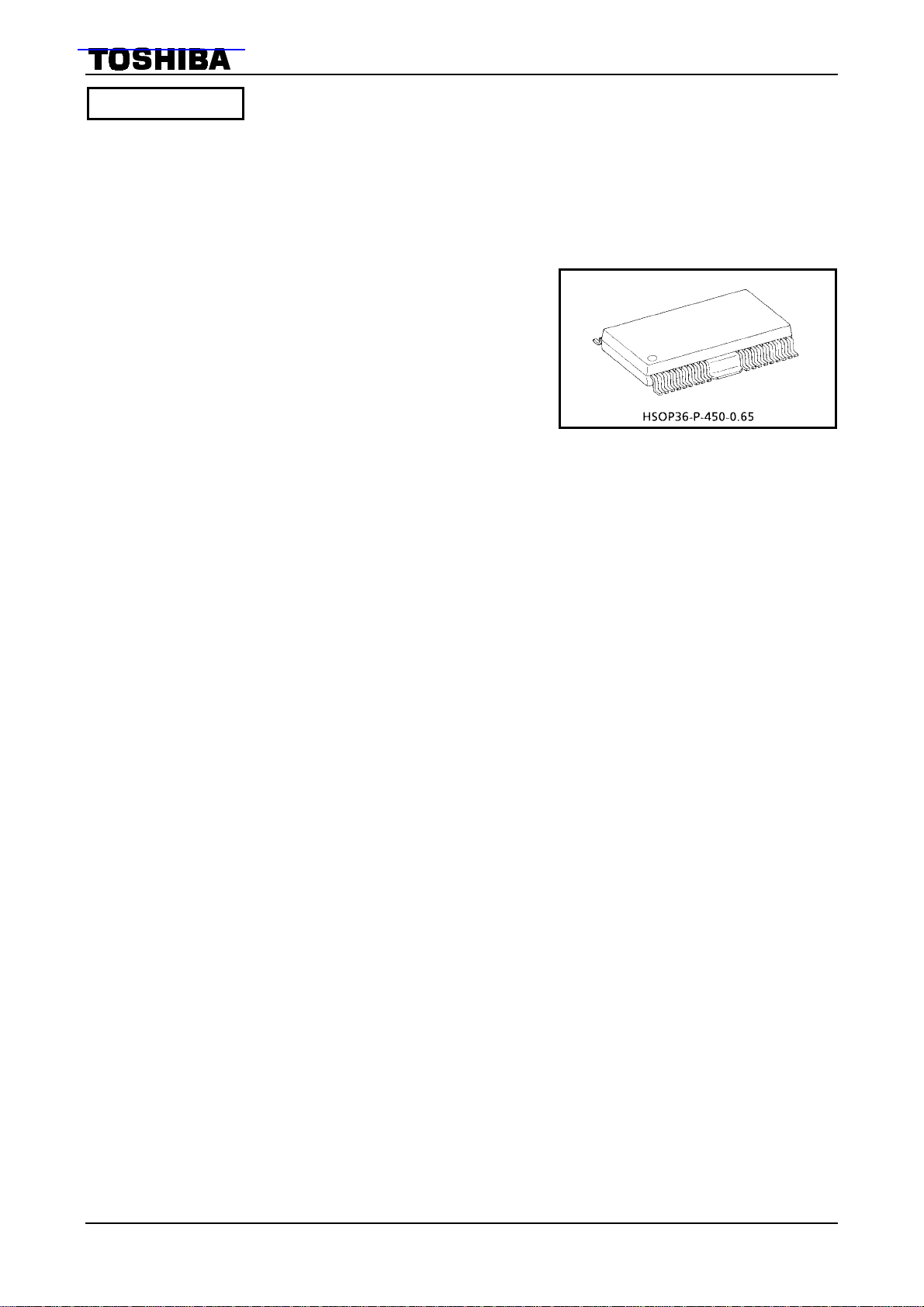
• 36-pin power flat package (HSOP36-P-450-0.65)
• Output voltage: 40 V max
• Output current: 1.8 A/phase max
• 2-phase, 1-2 (type 2) phase, W1-2 phase, 2W1-2 phase, 4W1-2 phase, or motor lock mode can be selected.
• Built-in Mixed Decay mode enables specification of four-stage attenuation ratio.
• Chopping frequency can be set by external resistors and capacitors.
High-speed chopping possible at 100 kHz or higher.
Note: When using the IC, pay attention to thermal conditions. These devices are easy damage by high static
voltage. In regards to this, please handle with care.
= 0.5 Ω (Tj = 25°C @1.0 A: typ.)
on
&VM power monitor (reset) circuit for protection
DD
1
2001-09-05
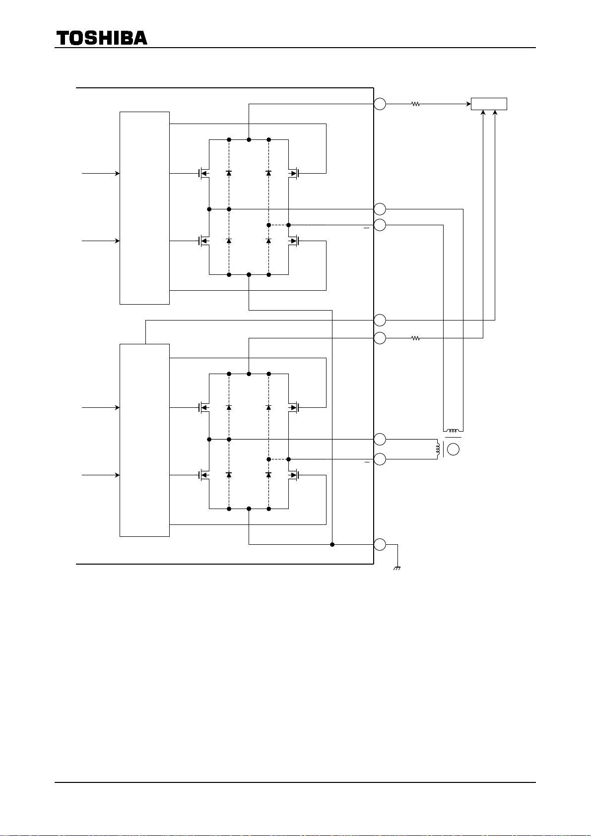
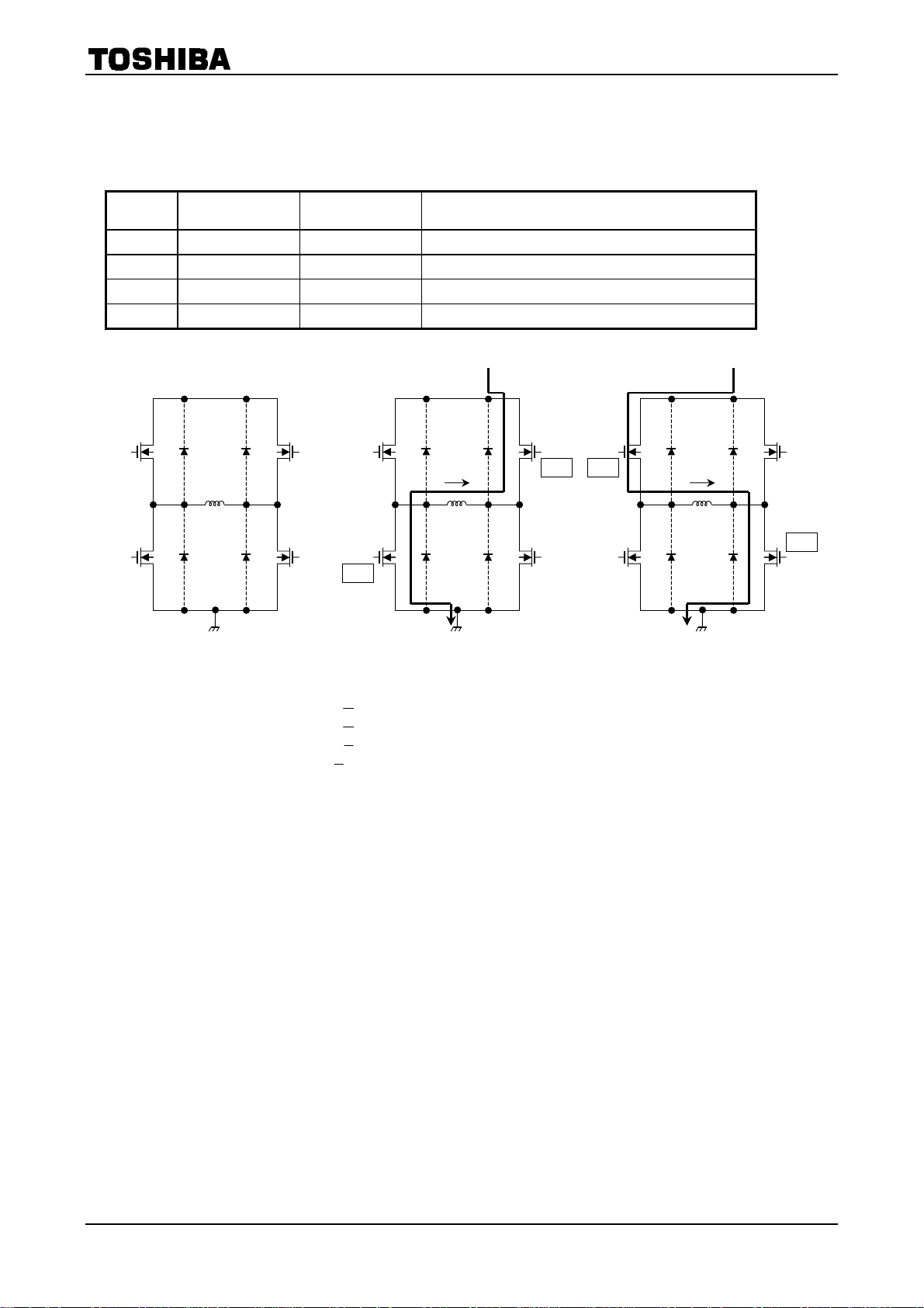
Block Diagram
f
1. Overview
TB62209F
RESET
CW/CCW
ENABLE
STANDBY
D MODE 3
D MODE 2
D MODE 1
CLK
V
re
TORQUE 1
Current Level Set
TORQUE 2 MDT 1 MDT 2
Micro-step decorder
Torque control
4-bit DA
(sine angle control)
V
DD
Chopper OSC
OCS
CR-CLK
converter
MO
CR
V
M
Ccp C
Ccp B
Ccp A
Current Feedback (×2)
V
R
S
V
M
Charge
Pump
Unit
RS 1
V
RS 2
STANDBY
ENABLE V
R
S COMP 1
R
S COMP 2
(Mixed Decay control)
Output (H-bridge)
× 2
Stepping
Moter
Output control
ISD
V
DDR/VMR
V
M
protect
Protection Unit
TSD
DD
TSD
protect
2
2001-09-05
2. LOGIC UNIT A/B (C/D unit is the same as A/B unit)
Function
This circuit is used to input from the DATA pins micro-step current setting
them to the subsequent stage. By switching the SETUP pin, the data in the mixed decay
can be overwritten.
MDT 1 MDT 2
TORQUE 1 TORQUE 2
TB62209F
data and to transfer
timing table
DATA MODE
D MODE 1
D MODE 2
D MODE 3
CW/CCW
CLK
STANDBY
RESET
ENABLE
Output
control
circuit
Torque
× 2 bits
Current
feedback
circuit
Micro-step decoder
Decay
× 2 bits
B unit side
Mixed
Decay
circuit
Micro-step
current data
× 4 bits
B unit side
DA circuit
Phase
× 1 bit
B unit side
Output
control
circuit
Decay
× 2 bits
A unit side
Micro-step
current data
× 4 bits
A unit side
Phase
× 1 bit
A unit side
3
2001-09-05

3. Current feedback circuit and current setting circuit
Function
The current setting circuit is used to set the reference voltage of the output current using the current
setting decoder.
The current feedback circuit is used to output to the output control circuit the relation between the
set current value and
current setting circuit with the potential difference generated when current flows through the current
sense resistor connected between R
The chopping waveform generator circuit to which CR is connected is used to generate clock used as
reference for the chopping frequency.
TORQUE
0, 1
output current. This is done by comparing the reference voltage output to the
and VM.
S
Decoder
Unit
CURRENT
0-3
TB62209F
V
ref
R
S
100%
85%
70%
50%
Torque
control
circuit
Current setting
circuit
DA circuit
VRS circuit 1
(detects
potential
difference
between
RS and VM)
Micro-step
15
current
14
setting
13
selector
12
11
circuit
10
9
8
7
6
5
4
4-bit
3
DA
2
circuit
1
0
R
S COMP
circuit
1
(Note 1)
Chopping waveform
Waveform shaping circuit
Chopping reference circuit
Output stop signal (ALL OFF)
generator circuit
<Use in Charge mode>
NF
(set current
reached signal)
CR
Mixed
Decay
timing
circuit
Output
control
circuit
V
M
Current feedbackcircuit
VRS circuit 2
(detects
potential
difference
between
VM and RS)
R
S COMP
circuit
2
(Note 2)
RNF
(set current
monitor signal)
<Use in FAST MODE>
Note 1: R
S COMP1
: Compares the set current with the output current and outputs a signal when the output
current reaches the set current.
Note 2: R
S COMP2
: Compares the set current with the output current at the end of Fast mode during chopping.
Outputs a signal when the set current is below the output current.
4
2001-09-05
4. Output control circuit, current feedback circuit and current setting circuit
TB62209F
Current
feedback
circuit
Current
setting
circuit
STANDBY
Output pin
V
V
DD
Output control circuit
NF set current
reached signal
RNF set current
monitor signal
Output stop
signal
ISD
circuit
M
VMR
circuit
V
DDR
circuit
Micro-step current setting
decoder circuit
PHASE
Mixed
Decay
timing
Charge Start
U1
U2
L1
L2
Output RESET signal
Internal
stop
signal
select
circuit
Charge
DECAY
MODE
pump
halt
signal
CR counter
CR Serector
VDD VM
Charge
pump
circuit
Chopping
reference circuit
Mixed
Decay
timing
circuit
Power supply for
upper drive output
VH
Output circuit
Output
circuit
Cop A
Cop B
V
: VDD power on
DDR
Reset
VMR: VM power on Reset
ISD: Current shutdown
circuit
TSD: Thermal shutdown
circuit
Note: The STANDBY pins are pulled down in the IC by 10-kΩ resistor.
When not using the pin, connect it to GND. Otherwise, malfunction may occur.
TSD
circuit
Protection
circuit
Micro-step current
setup latch
clear signal
LOGIC
Mixed Decay
timing table clear
signal
5
Cop C
2001-09-05
5. Output equivalent circuit (A/B unit (C/D unit is the same as A/B unit)
TB62209F
From output
control
circuit
From output
control
circuit
Power
supply
for upper
drive output
(VH)
U1
U2
L1
L2
Output
driver
circuit
Phase A
Power
supply
for upper
drive output
(VH)
U1
U2
L1
L2
Output
driver
circuit
Phase B
U1
L1
U1
L1
U2
L2
U2
L2
Output A
Output
Output B
Output
R
S A
A
RSB
B
R
RS A
V
M B
R
RS B
PGND
To VM
M
Note: The diode on the dotted line is parasitic diode.
6
2001-09-05
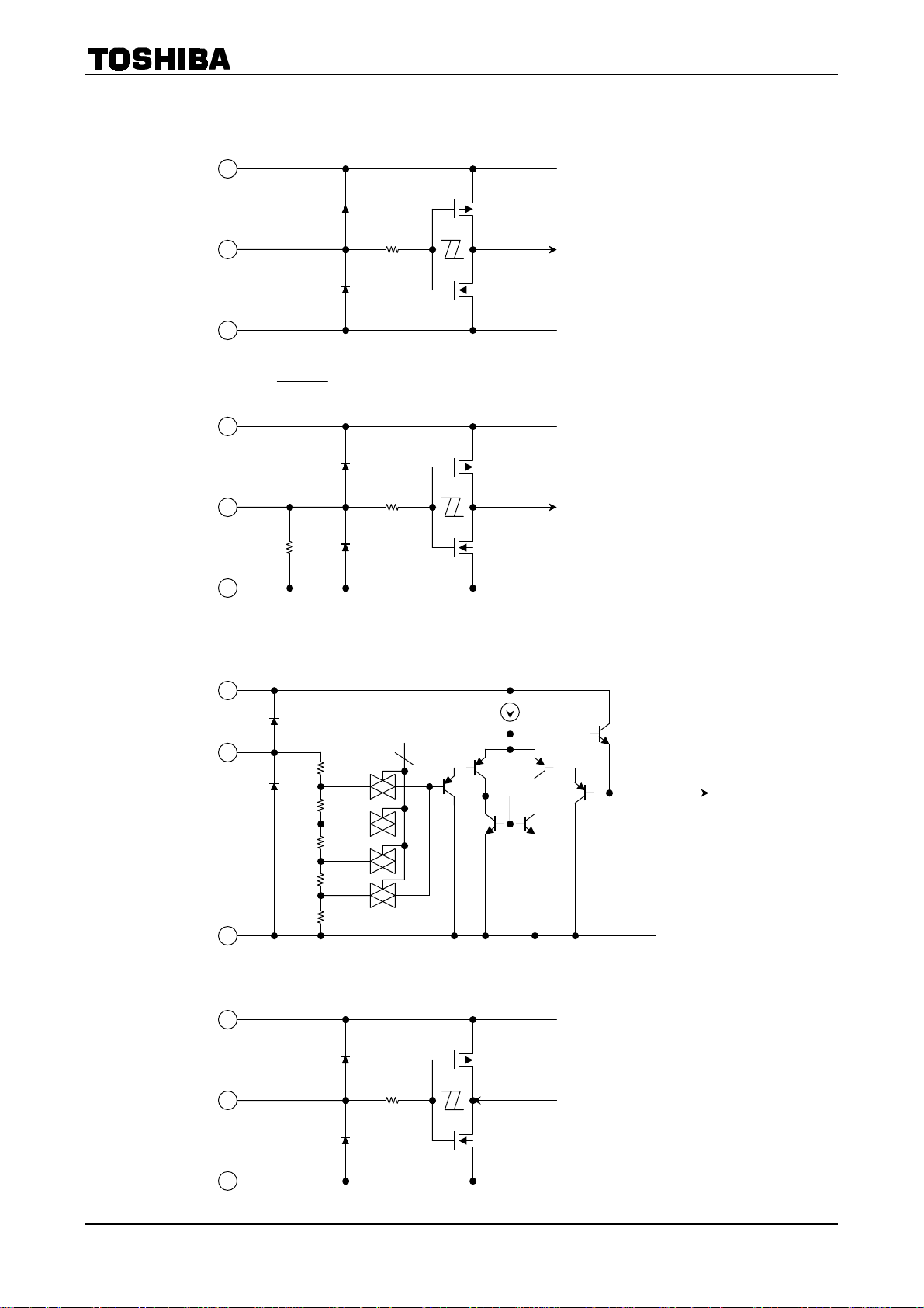
6. Input equivalent circuit
1. Input circuit (CLK, TORQUE, MDT, CW/CCW, DATA MODE, Decay Mode)
V
DD
IN
150 Ω
To Logic IC
TB62209F
2. Input circuit (
3. V
V
SS
V
DD
IN
V
SS
input circuit
ref
V
DD
IN
RESET
100 kΩ
, ENABLE, STANDBY)
150 Ω
2
GND
To Logic IC
GND
V
SS
4. Output circuit (MO, PROTECT)
V
DD
OUT
V
SS
150 Ω
To DA circuit
GND
GND
7
2001-09-05
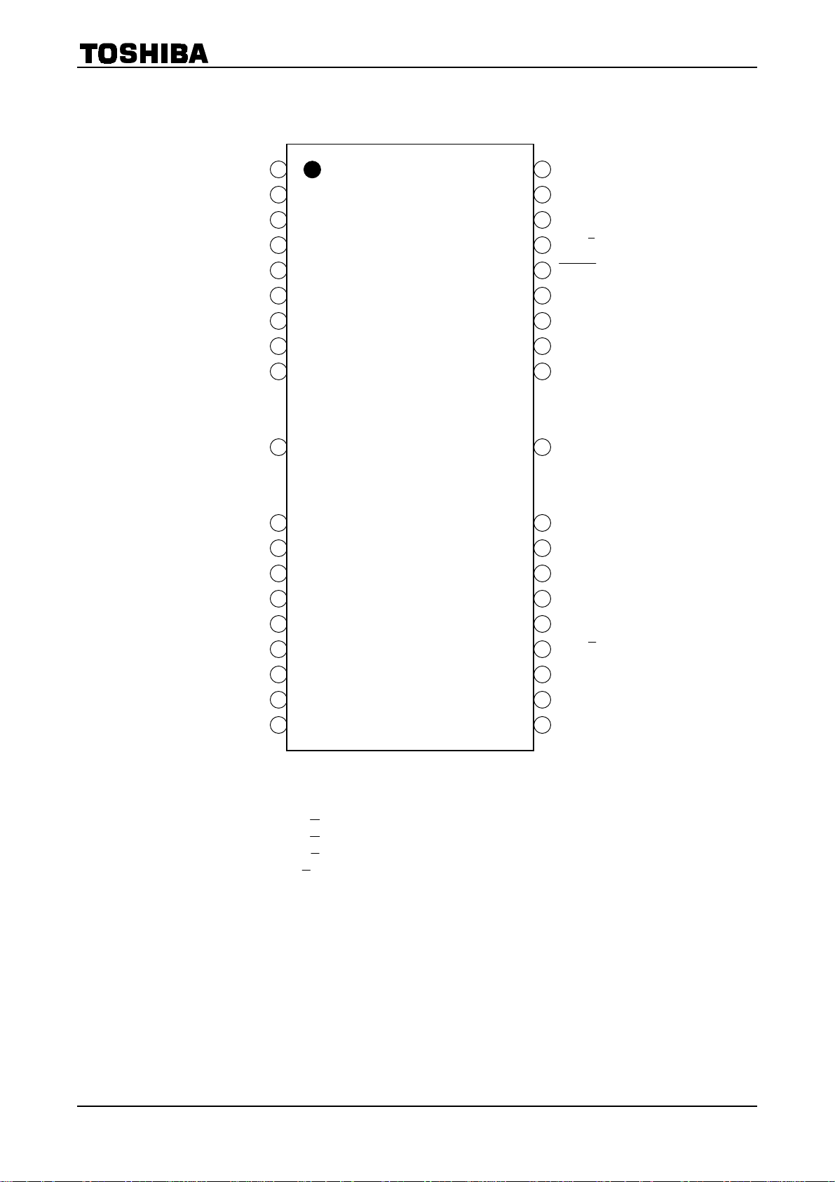
TB62209F
f
Y
Pin Assignment
(top view)
DD
re
S B
1 D MODE 1
2 D MODE 2
3 D MODE 3
4 CW/CCW
5 V
6 V
7 NC
8 NC
9 R
(FIN)
TB62209F
36
CR
35
CLK
34 ENABLE
33 OUT B
32 RESET
31 DATA MODE
30 NC
29 OUT B
28 PGND
(FIN)
10R
S A
11NC
12NC
13VM
14STANDB
15Ccp A
16Ccp B
17Ccp C
18MO
Pin Assignment for PWM in Data Mode
D MODE 1 → GA+ (OUT A, A)
D MODE 2 → GA− (OUT A,
D MODE 3 → GB+ (OUT B,
CW/CCW → GB− (OUT B,
Note: Pin assignment above is different at data mode and PWM.
A)
B)
B)
27 PGND
26 OUT A
25 NC
24 MDT 2
23 MDT 1
22 OUT A
21 TORQUE2
20 TORQUE1
19 PROTECT
8
2001-09-05
Pin Description 1
Pin Number Symbol Function Remarks
D MODE 3, 2, 1 =
1 D MODE 1
2 D MODE 2
3 D MODE 3
4 CW/CCW Sets motor rotation direction
5 VDD Logic power supply connecting pin Connect to logic power supply (5 V).
6 V
7 NC Not connected Not wired
8 NC Not connected Not wired
9 R
FIN FIN FIN Logic ground pin
10 R
11 NC Not connected Not wired
12 NC Not connected Not wired
ref
S B
S A
Motor drive mode setting pin
Reference power supply pin for setting output
current
Unit-B power supply pin
(connecting pin for power detection resistor)
Unit-A power supply pin
(pin connecting power detection resistor)
LLL: Same function as that of STANDBY pin
LLH: Motor Lock mode
LHL: 2-Phase Excitation mode
LHH: 1-2 Phase Excitation (A) mode
HLL: 1-2 Phase Excitation (B) mode
HLH: W1-2 Phase Excitation mode
HHL: 2W1-2 Phase Excitation mode
HHH: 4W1-2 Phase Excitation mode
CW: Forward rotation
CCW: Reverse rotation
Connect to supply voltage for setting current.
Connect current sensing resistor between this
pin and V
Connect to power ground.
The pin functions as a heat sink. Design pattern
taking heat into consideration.
Connect current sensing resistor between this
pin and V
.
M
.
M
Pin Assignment for PWM in Data Mode
TB62209F
D MODE 1 → GA+ (OUT A, A)
D MODE 2 → GA− (OUT A,
D MODE 3 → GB+ (OUT B,
CW/CCW → GB− (OUT B,
A)
B)
B)
9
2001-09-05

Pin Description 2
Pin Number Symbol Function Remarks
13 VM Motor power supply monitor pin Connect to motor power supply.
14
15 Ccp A
16 Ccp B
17 Ccp C (charging side)
18 MO Electrical angle (0°) monitor pin
19 PROTECT TSD operation detector pin
20 TORQUE 1
21 TORQUE 2
22 OUT A Channel A output pin
23 MDT 2
24 MDT 1
STANDBY
All-function-initializing and Low Power
Dissipation mode pin
Pin connecting capacitor for boosting output
stage drive power supply (storage side
connected to GND)
Pin connecting capacitor for boosting output
stage drive power supply
Motor torque switch setting pin
Mixed Decay mode setting pins
H: Normal operation
L: Operation halted
Charge pump output halted
Connect capacitor for charge pump (storage
side) V
Connect capacitor for charge pump (charging
side) between this pin and Ccp C.
Connect capacitor for charge pump (charging
side between this pin and Ccp B.
Outputs High level in 4W1-2, 2W1-2, W1-2, or
1-2 Phase Excitation mode with electrical angle
of 0° (phase B: 100%, phase A: 0%).
In 2-Phase Excitation mode, outputs High level
with electrical angle of 0° (phase B: 100%,
phase A: 100%).
Detects thermal shut down (TSD) and outputs
High level.
Torque 2, 1 = HH: 100%
LH: 85%
HL: 70%
LL: 50%
MDT 2, 1 = HH: 100%
HL: 75%
LH: 37.5%
LL: 12.5%
and VDD are generated.
M
TB62209F
10
2001-09-05

Pin Description 3
Pin Number Symbol Function Remarks
25 NC Not connected Not wired
26 OUT A Channel A output pin
27 PGND Power ground pin Connect all power ground pins and VSS to GND.
FIN FIN Logic ground pin
28 PGND Power ground pin Connect all power ground pins to GND.
29 OUT B Channel B output pin
30 NC Not connected Not wired
31 DATA MODE Clock input and PWM
32 RESET Initializes electrical angle.
33 OUT B Channel B output pin
34 ENABLE Output enable pin Forcibly turns all output transistors off.
35 CLK
36 CR
Inputs CLK for determining number of motor
rotations.
Chopping reference frequency reference pin (for
setting chopping frequency)
The pin functions as a heat sink. Design pattern
taking heat into consideration.
H: Controls external PWM.
L: CLK-IN mode
We recommend this pin normally be used as
CLK-IN mode pin (Low).
In PWM mode, functions such as constant
current control do not operate.
Forcibly initializes electrical angle.
At this time we recommend ENABLE pin be set
to Low to prevent misoperation.
H: Resets electrical angle.
L: Normal operation
Electrical angle is incremented by one for each
CLK input.
CLK is reflected at rising edge.
Determines chopping frequency.
TB62209F
11
2001-09-05

1. Function of CW/CCW
CW/CCW switches the direction of stepping motor rotation.
Input Function
H Forward (CW)
L Reverse (CCW)
2. Function of MDT 1/MDT 2
MDT 1/MDT 2 specifies the current attenuation speed at constant current control.
The larger the rate (%), the larger the attenuation of the current. Also, the peak current value (current
ripple) becomes larger. (Typical value is 37.5%.)
MDT 2 MDT 1 Function
L L 12.5% Mixed Decay mode
L H 37.5% Mixed Decay mode
H L 75% Mixed Decay mode
H H 100% Mixed Decay mode (Fast Decay mode)
3. Function of TORQUE X
TORQUE X changes the current peak value in four steps. Used to change the value of the current used,
for example, at startup and fixed-speed rotation.
TB62209F
TORQUE 2 TORQUE 1 Comparator Reference Voltage
H H 100%
L H 85%
H L 70%
L L 50%
4. Function of RESET (forced initialization of electrical angle)
With the CLK input method (decoder method), unless CLKs are counted, except MO, where the electrical
angle is at that time is not known. Thus, this method is used to forcibly initialize the electrical angle.
For example, used to change the excitation mode to another drive mode during output from MO
(electrical angle = 0°).
Input Function
H Initializes electrical angle to 0°
L Normal operation
12
2001-09-05
5. Function of ENABLE (output operation)
ENABLE forcibly turns OFF all output transistors at operation.
Data such as electrical angle and operating mode are all retained.
Input Function
H Operation enabled (active)
L
Output halted (operation other
than output active)
6. Function of STANDBY
STANDBY halts the charge pump circuit (power supply booster circuit) as well as halting output.
We recommend setting to Standby mode at power on.
(At this time, data on the electrical angle are retained.)
Input Function
H Operation enabled (active)
Output halted (Low Power
L
Dissipation mode)
Charge pump halted
7. Functions of Excitation Modes
TB62209F
Excitation Mode DM3 DM2 DM1 Remarks
1
2 Motor Lock mode 0 0 1 Locks only at 0° electrical angle.
3
4
5
6
7
8
Low Power
Dissipation mode
2-Phase Excitation
mode
1-2 Phase Excitation
(A)
1-2 Phase Excitation
(B)
W1-2 Phase
Excitation
2W1-2 Phase
Excitation
4W1-2 Phase
Excitation
0 0 0
0 1 0 45° → 135° → 225° → 315° → 45°
0 1 1 Low-torque, 1-bit micro-step change
1 0 0 High-torque, 1-bit micro-step change
1 0 1 2-bit micro-step change
1 1 0 3-bit micro-step change
1 1 1 4-bit micro-step change
Standby mode
Charge pump halted
13
2001-09-05
8. Function of DATA MODE
DATA MODE switches external duty control (forced PWM control) and constant current CLK-IN control.
In Phase mode, H-bridge can be forcibly inverted and output only can be turned off. Constant current drive
including micro-step drive can only be controlled in CLK-IN mode.
Input Function
H PHASE MODE
L CLK-IN MODE
Note 1: Normally, use CLK-IN mode.
9. Electrical Angle Setting immediately after Initialization
In Initialize mode (immediately after RESET is released), the following currents are set.
In Low Power Dissipation mode, the internal decoder continues incrementing the electrical angle but
current is not output.
Note that the initial electrical angle value in 2-Phase Excitation mode differs from that in nW1-2 (n = 0,
1, 2, 4) Phase Excitation mode.
Excitation Mode IB (%) IA (%) Remarks
TB62209F
1
2 Motor Lock mode 100 0
3 2-Phase Excitation 100 100 45°
4
5
6
7
8
Low Power
Dissipation mode
1-2 Phase Excitation
(A)
1-2 Phase Excitation
(B)
W1-2 Phase
Excitation
2W1-2 Phase
Excitation
4W1-2 Phase
Excitation
100 0 Electrical angle incremented but no current output
Electrical angle incremented but no motor rotation
due to no IA output
100 0 0°
100 0 0°
100 0 0°
100 0 0°
100 0 0°
Note 2: Where, IB = 100% and IA = 0%, the electrical angle is 0°. Where, IB = 0% and IA = 100%, the electrical
angle is +90°.
14
2001-09-05
10. Function of DATA MODE (Phase A mode used for explanation)
DATA MODE inputs the external PWM signal (duty signal) and controls the current. Functions such as
constant current control and overcurrent protector do not operate.
Use this mode only when control cannot be performed in CLK-IN mode.
GA+ GA− Output State
(1) L L Output off
(2) L H A+ phase: Low A− phase: High
(3) H L A+ phase: High A− phase: Low
(4) H H Output off
(1)・(4)
(2)
TB62209F
(3)
U1
OFF
L1
OFF
PGND
Note: Output is off at (1) and (4).
D MODE 1 → GA+ (OUT A,
D MODE 2 → GA− (OUT A,
D MODE 3 → GB+ (OUT B,
CW/CCW → GB− (OUT B,
U2
OFF
L2
OFF
A)
A)
B)
B)
U1
OFF
L1
ON
(Note)
Load
PGND
U2
ON
L2
OFF
U1
ON
OFF
L1
(Note)
Load
U2
OFF
ON
L2
PGND
15
2001-09-05
TB62209F
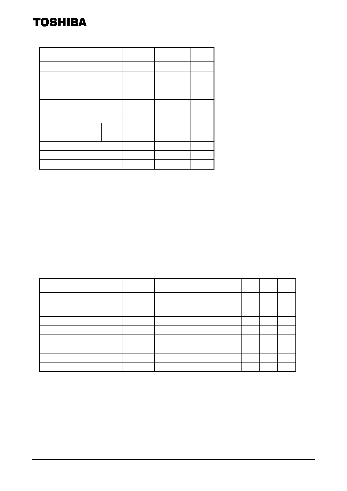
Maximum Ratings
Characteristics Symbol Rating Unit
Logic supply voltage V
Motor supply voltage VM 40
Output current (Note 1) I
Current detect pin voltage VRS V
Charge pump pin maximum voltage
(CCP1 Pin)
Logic input voltage (Note 2) VIN to VDD + 0.4 V
Power dissipation
Operating temperature T
Storage temperature T
Junction temperature Tj 150 °C
(Ta ==== 25°C)
(Note 3) 1.4
(Note 4)
DD
1.8 A/phase
OUT
V
V
H
PD
−40 to 85 °C
opr
−55 to 150 °C
stg
7 V
± 4.5 V V
M
+ 7.0 V
M
3.2
W
V
Note 1: Perform thermal calculations for the maximum current value under normal conditions. Use the IC at 1.5 A or
less per phase.
The current velue maybe controled according to the ambient temperature or board conditions.
Note 2: Input 7 V or less as V
IN
.
Note 3: Measured for the IC only. (Ta = 25°C)
Note 4: Measured when mounted on the board. (Ta = 25°C)
Ta: IC ambient temperature
T
: IC ambient temperature when starting operation
opr
Tj: IC chip temperature during operation Tj (max) is controlled by TSD (thermal shut down circuit)
Recommended Operating Conditions
Characteristics Symbol Test Condition Min Typ. Max Unit
Power supply voltage VDD 4.5 5.0 5.5 V
Motor supply voltage VM
Output current I
Logic input voltage VIN GND VDD V
Clock frequency f
Chopping frequency f
Reference voltage V
Current detect pin voltage VRS VDD = 5.0 V 0 ±1.0 ±4.5 V
OUT (1)
CLK
chop
ref
(Ta ==== 0 to 85°C, (Note 5))
= 5.0 V, Ccp1 = 0.22 µF,
V
DD
Ccp2 = 0.02 µF
Ta = 25°C, per phase 1.2 1.5 A
VDD = 5.0 V 1.0 150 KHz
VDD = 5.0 V 50 100 150 KHz
VM = 24 V, Torque = 100% 2.0 3.0 VDD V
20 24 34 V
Note 5: Because the maximum value of Tj is 120°C, recommended maximum current usage is below 120°C.
16
2001-09-05

TB62209F
Electrical Characteristics1
(unless otherwise specified, Ta ==== 25°C, VDD ==== 5 V, VM ==== 24 V)
Characteristics Symbol
HIGH V
IN (H)
Input voltage
LOW V
Input hysteresis voltage V
Input current 1
IN (L)
IN (HIS)
I
Data input pins with resistor 1.0
IN (H)
I
35 50 75
IN (H)
I
IN (L)
I
DD1
Power dissipation (VDD Pin)
I
DD2
IM1
Power dissipation (VM Pin)
Output standby
current
Output bias
current
Output leakage
current
Upper I
Upper I
Lower I
IM2
I
M3
OH
OB
OL
HIGH
(Refer-
ence)
Comparator
reference
voltage ratio
MID
HIGH
MID
LOW
LOW V
Output current differential ∆I
Output current setting differential ∆I
V
RS (H)
V
RS (MH)
V
RS (ML)
RS (L)
OUT1
OUT2
RS pin current IRS
R
ON (D-S) 1
R
Output transistor drain-source
ON (D-S) 1
ON-resistance
R
ON (D-S) 2
R
ON (D-S) 2
Test
Circuit
2.0 VDD
Data input pins
Test Condition Min Typ. Max Unit
V
DD
+ 0.4
GND
− 0.4
GND 0.8
Data input pins 200 400 700 mV
Data input pins without resistor
1.0
V
= 5 V (STROBE,
DD
DATA = L),
Logic, output all off
Output OPEN, f
LOGIC ACTIVE, V
Charge Pump = charged
RESET
CLK
= L,
= 1.0 kHz
= 5 V,
DD
RESET
,
1.0 2.0 3.0
1.0 2.5 3.5
Output OPEN (STROBE,
, DATA = L),
RESET
= L, Logic, output all off,
RESET
1.0 2.0 3.0
Charge Pump = no operation
Output OPEN, f
LOGIC ACTIVE, V
V
= 24 V, Output off,
M
Charge Pump = charged
Output OPEN, f
LOGIC ACTIVE, 100 kHz
chopping (emulation), Output
CLK
CLK
= 1 kHz
= 5 V,
DD
= 4 kHz
2.0 4.0 5.0
10 13
OPEN,
Charge Pump = charged
V
= VM = 24 V, V
RS
STANDBY = H,
OUT
RESET
= 0 V,
= L
−200 −150 µA
CLK = L
= 0 V, STANDBY = H,
V
I
OUT
= L, CLK = L
RESET
= VM = CcpA = V
V
RS
= 24 V, LOGIC IN = ALL = L
V
= 3.0 V, V
ref
TORQUE = (H) = 100% set
= 3.0 V, V
V
ref
TORQUE = (MH) = 85% set
= 3.0 V, V
V
ref
TORQUE = (ML) = 70% set
= 3.0 V, V
V
ref
TORQUE = (L) = 50% set
OUT
(Gain) = 1/5.0
ref
(Gain) = 1/5.0
ref
(Gain) = 1/5.0
ref
(Gain) = 1/5.0
ref
Differences between output
current channels
= 1000 mA −5 5 %
OUT
= 24 V, VM = 24 V
V
RS
= L (RESET state)
RESET
I
= 1.0 A, VDD = 5.0 V
OUT
T
= 25°C, Drain-Source
j
I
= 1.0 A, VDD = 5.0 V
OUT
T
= 25°C, Source-Drain
j
I
= 1.0 A, VDD = 5.0 V
OUT
T
= 105°C, Drain-Source
j
= 1.0 A, VDD = 5.0 V
I
OUT
T
= 105°C, Source-Drain
j
−100 −50 µA
1.0 1.0 µA
100
83 85 87
68 70 72
48 50 52
−5 5 %
1 2 µA
0.5 0.6
0.5 0.6
0.6 0.75
0.6 0.75
V
µA
mA
mA
%
Ω
17
2001-09-05

TB62209F
Electrical Characteristics 2
Characteristics Symbol
Chopper current Vector
(Ta ==== 25°C, VDD ==== 5 V, VM ==== 24 V, I
==== 1.0 A)
OUT
Test
Circuit
Test Condition Min Typ. Max Unit
θA = 90 (θ16) 100
θA = 84 (θ15) 100
θA = 79 (θ14) 93 98
θA = 73 (θ13) 91 96
θA = 68 (θ12) 87 92 97
θA = 62 (θ11) 83 88 93
θA = 56 (θ10) 78 83 88
θA = 51 (θ9) 72 77 82
θA = 45 (θ8) 66 71 76
θA = 40 (θ7) 58 63 68
θA = 34 (θ6) 51 56 61
θA = 28 (θ5) 42 47 52
θA = 23 (θ4) 33 38 43
θA = 17 (θ3) 24 29 34
θA = 11 (θ2) 15 20 25
θA = 6 (θ1) 5 10 15
θA = 0 (θ0)
%
0
18
2001-09-05

TB62209F
Electrical Characteristics 3 (unless otherwise specified, Ta ==== 25°C, VDD ==== 5 V, VM ==== 24 V)
Characteristics Symbol
V
input voltage V
ref
V
input current I
ref
V
attenuation ratio V
ref
TSD temperature (Note 1) TjTSD VDD = 5 V, VM = 24 V 130 170 °C
TSD return temperature difference
(Note 1)
VDD return voltage V
VM return voltage VMR 11 VDD = 5 V, STANDBY = H 2.0 3.5 5.0 V
Over current protected circuit
operation current (Note 2)
High temperature monitor pin
output current
Electrical angle monitor pin output
current
High temperature monitor pin
output voltage
Electrical angle monitor pin output
voltage
ref
ref
(GAIN)
ref
∆T
TSD TjTSD = 130 to 170°C
j
DDR
ISD V
I
protect
I
MO
V
protect (H)
V
protect (L)
V
MO2 (H)
V
MO2 (L)
Test
Circuit
9
9
10 VM = 24 V, STANDBY = H 2.0 3.0 4.0 V
12
12
12
12
Test Condition Min Typ. Max Unit
= 24 V, VDD = 5 V,
V
M
STANDBY = H,
Output on, CLK = 1 kHz
STANDBY = H,
Output off, V
V
= 5 V, V
DD
V
= 24 V, VDD = 5 V,
M
STANDBY = H,
Output on, V
− 1.0 V
= 5 V, VM = 24 V 3.0 A
DD
= 5 V,
V
DD
TSD = operating condition
= 5 V,
V
DD
electrical angle = 0°
(IB = 100%, IA = 0%)
= 5 V,
V
DD
TSD = operating condition
= 5 V,
V
DD
TSD = not operating
condition
V
= 5 V,
DD
electrical angle = except 0°
(IB = 100%, IA = Except 0%
set)
= 5 V,
V
DD
electrical angle = 0°
(IB = 100%, IA = 0%)
RESET = L,
RESET
= 24 V,
M
= 3.0 V
ref
RESET
= 2.0 to VDD
ref
2.0 V
= L,
20 35 50 µA
= L,
1/4.8 1/5.0 1/5.2
TSD
T
TjTSD
j
− 50
− 35
1.0 3.0 5.0 mA
1.0 3.0 5.0 mA
DD
TjTSD
− 20
V
°C
V
V
Note 1: Thermal shut down (TSD) circuit
When the IC junction temperature reaches the specified value and the TSD circuit is activated, the internal
reset circuit is activated switching the outputs of both motors to off.
When the temperature is set between 130 (min) to 170°C (max), the TSD circuit operates.
When the TSD circuit is activated, the charge pump is halted, and TROTECT pin outputs V
Even if the TSD circuit is activated and Standby goes H → L → H instantaneously, the IC is not reset until
the IC junction temperature drops −20°C (typ.) below the TSD operating temperature (hysteresis function).
Note 2: Overcurrent protection circuit
When current exceeding the specified value flows to the output, the internal reset circuit is activated, and the
ISD turns off the output.
Until the Standby signal goes Low to High, the overcurrent protection circuit remains activated.
During ISD, IC turns Standby mode and the charge pump halts.
19
voltage.
DD
2001-09-05

TB62209F
AC Characteristics
Characteristics Symbol
Clock frequency f
Minimum clock pulse width
Output transistor switching
characteristic
Transistor switching characteristics
(MO, PROTECT)
Noise rejection dead band time t
CR reference signal oscillation
frequency
Chopping frequency range
Chopping frequency f
Charge pump rise time t
(Ta ==== 25°C, VM ==== 24 V, VDD ==== 5 V, 6.8 mH/5.7 ΩΩΩΩ)
Test
Circuit
120 kHz
CLK
tw (t
) 100
CLK
twp 50
t
50
wn
tr Output Load: 6.8 mH/5.7 Ω 100
tf 100
t
CLK to OUT 1000
pLH
t
Output Load: 6.8 mH/5.7 Ω 2000
pHL
t
CR to OUT 500
pLH
Output Load: 6.8 mH/5.7 Ω 1000
t
pHL
tr 20
tf 20
t
20
pLH
20
t
pHL
I
BRANK
f
C
CR
f
chop (min)
f
chop (max)
chop
ONG
Test Condition Min Typ. Max Unit
= 1.0 A 200 300 400 ns
OUT
= 560 pF, R
osc
V
= 24 V, VDD = 5 V,
M
Output ACTIVE (I
Step fixed, Ccp1 = 0.22 µF,
Ccp2 = 0.01 µF
Output ACTIVE (I
CR CLK = 800 kHz
Ccp = 0.22 µF, Ccp = 0.01 µF
VM = 24 V, VDD = 5 V,
STANDBY = ON → OFF
= 3.6 kΩ 800 kHz
osc
= 1.0 A)
OUT
OUT
= 1.0 A),
40 100 150 kHz
100 kHz
100 200 µs
µs
ns
ns
20
2001-09-05

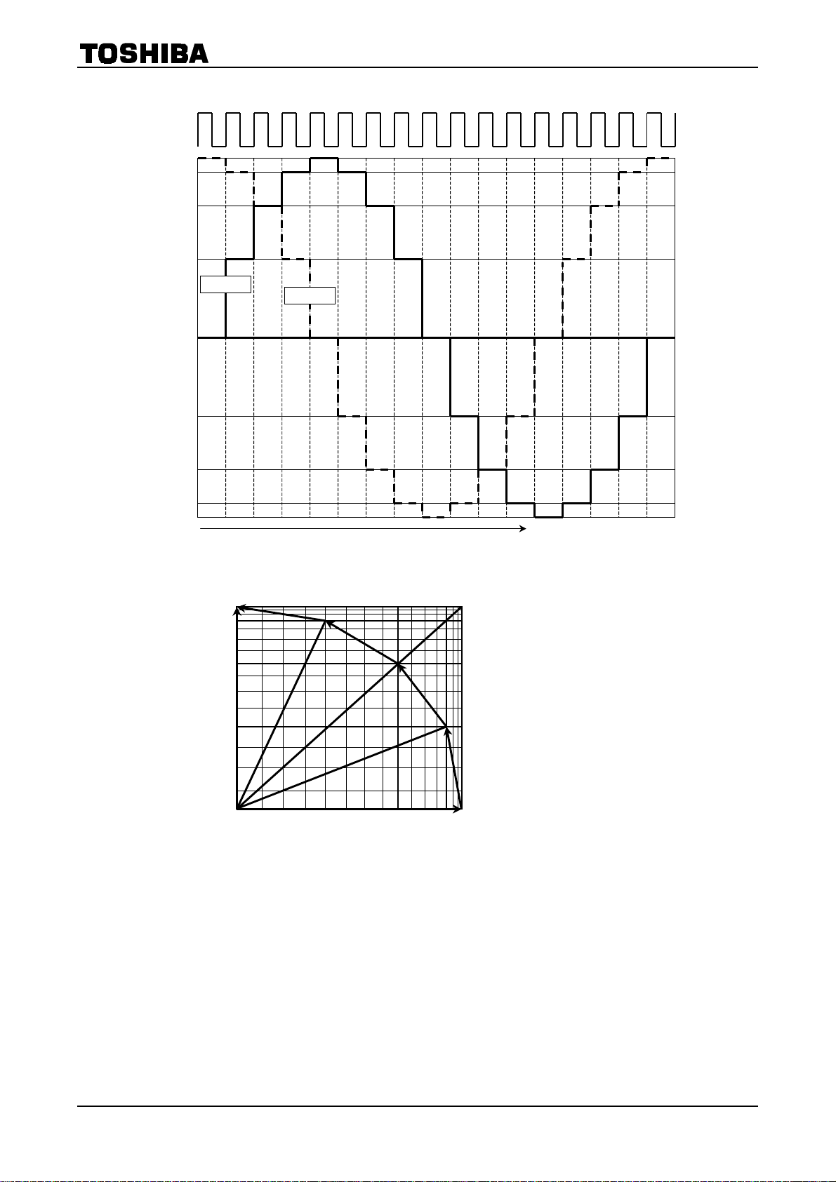
1. Current Waveform and Setting of Mixed Decay Mode
At constant current control, in current amplitude (pulsating current) Decay mode, a point from 0 to 3 can
be set using 2-bit parallel data.
NF is the point where the output current reaches the set current value. RNF is the timing for monitoring
the set current.
The smaller the MDT value, the smaller the current ripple (peak current value). Note that current decay
capability deteriorates.
f
CR pin
internal
CLK
waveform
DECAY MODE 0
12.5%
MIXED
DECAY
MODE
NF
Charge mode → NF: set current value reached → Slow mode
→ Mixed decay timing → Fast mode → current monitored
(when set current value > output current) Charge mode
chop
Set current value
TB62209F
MDT
RNF
37.5%
MIXED
DECAY
MODE
DECAY MODE 2
75%
MIXED
DECAY
MODE
DECAY MODE 3
FAST
DECAY
MODE
NF
Charge mode → NF: set current value reached → Slow mode
→ Mixed decay timing → Fast mode → current monitored
(when set current value > output current) Charge mode
NF
MDT
Charge mode → NF: set current value reached → Slow mode
→ Mixed decay timing → Fast mode → current monitored
(when set current value > output current) Charge mode
MDT
Set current value DECAY MODE 1
Set current value
Set current value
RNF
RNF
RNF
Fast mode → RNF: current monitored (when set current value
> output current) Charge mode → Fast mode
100% 75% 50% 25% 0
RNF
21
2001-09-05

2. CURRENT MODES
(MIXED ((((SLOW ++++ FAST) DECAY MODE Effect)
• Current value in increasing (Sine wave)
Set current
value
Sine wave in decreasing (When using MIXED DECAY Mode with large attenuation ratio (MDT%) at
attenuation)
Set current
value
Slow Slow
Set current
Slow Slow
Fast Charge
Charge
value
Fast Charge
Fast
TB62209F
Slow
Fast
Charge
Because current attenuates so quickly, the current
immediately follows the set current value.
Charge
Slow
Fast
Set current
value
Charge
Fast
Set current
value
Slow
Fast
Charge
Slow
Fast
• Sine wave in decreasing (When using MIXED DECAY Mode with small attenuation ratio (MDT%) at
attenuation)
Because current attenuates slowly, it takes a long time
for the current to follow the set current value (or the
current does not follow).
Fast
Charge
Fast
Charge
Fast
Charge
Slow
Fast
Slow
Charge
Set current
value
If RNF, current watching point, was the set current value (output current) in the mixed decay mode and
in the fast decay mode, there is no charge mode but the slow + fast mode (slow to fast is at MDT) in the
next chopping cycle.
Note: The above charts are schematics. The actual current transient responses are curves.
22
2001-09-05

3. MIXED DECAY MODE waveform (Current Waveform)
TB62209F
Internal
CR CLK
signal
I
OUT
Set current
value
25%
MIXED
DECAY
MODE
I
OUT
f
f
chop
NF
MDT (MIXED DECAY TIMING) point
• When NF is after MIXED DECAY TIMING
f
f
chop
Set current value
RNF
Fast Decay mode after Charge mode
Set current value
NF
chop
chop
NF
Set current
value
25%
MIXED
DECAY
MODE
Set current
value
I
OUT
25%
MIXED
DECAY
MODE
MDT (MIXED DECAY TIMING) point
NF
NF
CLK signal input
• In MIXED DECAY MODE, when the output current > the set current value
f
f
chop
NF
RNF
Set current value
f
chop
Because the set current value is the output
current, no CHARGE MODE in the next cycle.
(Charge cancel function)
RNF
MDT (MIXED DECAY TIMING) point
chop
RNF
NF
CLK signal input
23
2001-09-05

4. FAST DECAY MODE waveform
f
chop
Set current
value
I
OUT
TB62209F
FAST
DECAY
MODE
(100%
MIXED
DECAY
MODE)
Because the set current value is the output
current, FAST DECAY MODE in the next
cycle. (Charge cancel function)
RNF
Because the set current value is the output
current, CHARGE MODE → NF → FAST
DECAY MODE in the next cycle.
CLK signal input
Set current value
RNF
NF
The output current to the motor is in supply voltage mode after the current value set by V
Torque reached at the set current value.
RNF
, RRS, or
ref
24
2001-09-05

5. CLK SIGNAL, INTERNAL CR CLK, AND OUTPUT CURRENT waveform
g
(When CLK signal is input in SLOW DECAY MODE)
12.5% MIXED DECAY MODE
f
Internal
CR CLK
si
nal
f
chop
f
chop
chop
TB62209F
Set current value
I
OUT
NF
MDT
Set current value
NF
MDT
RNF
RNF
CLK signal input
Reset CR-CLK counter here
Momentarily enters CHARGE MODE
When CLK signal is input, the chopping counter (CR-CLK counter) is forced to reset at the next CR-CLK
timing.
Because of this, compared with a method in which the counter is not reset, response to the input data is
faster.
The delay time, the theoretical value in the logic portion, is expected to be a one-cycle CR waveform: 5 µs
at 100 kHz CHOPPING.
When the CR counter is reset due to CLK signal input, CHARGE MODE is entered momentarily due to
current comparison.
Note: In FAST DECAY MODE, too, CHARGE MODE is entered momentarily due to current comparison.
25
2001-09-05

6. STROBE SIGNAL, INTERNAL CR CLK, AND OUTPUT CURRENT waveform
(When CLK signal is input in CHARGE MODE)
12.5% MIXED DECAY MODE
f
Internal
CR CLK
signal
Set current
value
I
OUT
f
chop
f
chop
MDT
NF
Set current value
RNF
chop
MDT
TB62209F
RNF
CLK signal input
Reset CR-CLK counter here
Momentarily enters CHARGE MODE
26
2001-09-05

7. STROBE SIGNAL, INTERNAL CR CLK, AND OUTPUT CURRENT waveform
(When STROBE signal is input in FAST DECAY MODE)
12.5% MIXED DECAY MODE
f
Internal
CR CLK
signal
f
chop
f
chop
chop
TB62209F
Set current
value
I
OUT
NF
MDT
Set current value
MDT
NF
MDT
RNF
RNF
STROBE signal input
Reset CR-CLK counter here
Momentarily enters CHARGE MODE
27
2001-09-05

8. CLK SIGNAL, INTERNAL CR CLK, AND OUTPUT CURRENT waveform
(When CLK signal is input in 2 EXCITATION MODE)
12.5% MIXED DECAY MODE
f
Set current
value
I
OUT
f
chop
f
chop
chop
TB62209F
0
RNF
Set current value
CLK signal input
Reset CR-CLK counter here
NF
RNF
NF
MDT
28
2001-09-05

TB62209F
Current Discharge Path when
In Slow Mode, when all output transistors are forced to switch off, coil energy is discharged in the
following MODES:
Note: Parasitic diodes are located on dotted lines. In normal MIXED DECAY MODE, the current does not flow
to the parasitic diodes.
V
M
R
RS
RS pin
U1
ON
OFF
L1
(Note)
Load
PGND
U2
OFF
ON
L2
OFF
ENABLE
U1
ON
L1
Input During Operation
V
M
R
RS
RS pin
U2
(Note)
Load
PGND
OFF
Input
L2
ON
ENABLE
U1
OFF
L1
OFF
power supply
V
M
R
RS
RS pin
(Note)
Load
U2
OFF
L2
OFF
PGND
Charge mode Slow mode Forced OFF mode
As shown in the figure at right, an output transistor has parasitic diodes.
To discharge energy from the coil, each transistor is switched on allowing current to flow in the reverse
direction to that in normal operation. As a result, the parasitic diodes are not used. If all the output
transistors are forced to switch off, the energy of the coil is discharged via the parasitic diodes.
29
2001-09-05

Output Transistor Operating Mode
V
M
TB62209F
V
M
V
M
U1
ON
L1
OFF
R
RS
RS pin
U2
(Note)
Load
PGND
Charge mode Slow mode Fast mode
OFF
L2
ON
U1
OFF
L1
R
RS
RS pin
(Note)
Load
PGND
Output Transistor Operation Functions
CLK U1 U2 L1 L2
CHARGE ON OFF OFF ON
SLOW OFF OFF ON ON
FAST OFF ON ON OFF
U2
OFF
L2
ON
U1
OFF
L1
ON ON
R
RS pin
(Note)
Load
PGND
RS
U2
ON
L2
OFF
Note: The above table is an example where current flows in the direction of the arrows in the above figures.
When the current flows in the opposite direction of the arrows, see the table below.
CLK U1 U2 L1 L2
CHARGE OFF ON ON OFF
SLOW OFF OFF ON ON
FAST ON OFF OFF ON
30
2001-09-05

TB62209F
Power Supply Sequence
V
DD (max)
V
DD (min)
V
V
DD
V
M
Internal reset
DDR
GND
VM
V
M (min)
V
MR
GND
NON-RESET
RESET
(Recommended)
STANDBY
INPUT (Note 1)
STANDBY
H
L
Takes up to t
until operable.
ONG
Non-operable area
Note 1: If the V
drops to the level of the V
DD
or below while the specified voltage is input to the VM pin, the IC is
DDR
internally reset.
This is a protective measure against malfunction. Likewise, if the V
while regulation voltage is input to the V
, the IC is internally reset as a protective measure against
DD
drops to the level of the VMR or below
M
malfunction.
To avoid malfunction, when turning on V
or VDD, to input the Standby signal at the above timing is
M
recommended.
It takes time for the output control charge pump circuit to stabilize. Wait up to t
time after power on
ONG
before driving the motors.
Note 2: When the V
value is between 3.3 to 5.5 V, the internal reset is released, thus output may be on. In such a
M
case, the charge pump cannot drive stably because of insufficient voltage. The Standby state should be
maintained until V
reaches 13 V or more.
M
Note 3: Since VDD = 0 V and VM = voltage within the rating are applied, output is turned off by internal reset.
At that time, a current of several mA flows due to the Pass between V
When voltage increases on V
output, make sure that specified voltage is input.
DD
and VDD.
M
31
2001-09-05

How to Calculate Set Current
This IC controls constant current in CLK-IN mode.
At that time, the maximum current value (set current value) can be determined by setting the sensing
resistor (R
1/5.0 is V
) and reference voltage (V
RS
(max) OUT
(gain): V
ref
I
1
5.0
(V) V
ref
attenuation ratio. (For the specifications, see the electrical characteristics.)
ref
).
ref
××=
=
)Ω(
R
RS
50%) 70, 85, 100, (Torque Torque
For example, when inputting V
= 3 V and torque = 100% to output I
ref
or more) is required.
How to Calculate the Chopping and OSC Frequencies
At constant current control, this IC chops frequency using the oscillation waveform (saw tooth waveform)
determined by external capacitor and resistor as a reference.
The TB62209F requires an oscillation frequency of eight times the chopping frequency.
The oscillation frequency is calculated as follows:
TB62209F
100×
= 0.8 A, RRS = 0.75 Ω (0.5 W
OUT
=
f
CR
For example, when C
At this time, the chopping frequency f
f
= fCR/8 = 101
chop
When determining the chopping frequency, make the setting taking the above into consideration.
IC Power Dissipation
IC power dissipation is classified into two: power consumed by transistors in the output block and power
consumed by the logic block and the charge pump circuit.
• Power consumed by the Power Transistor (calculated with R
In Charge mode, Fast Decay mode, or Slow Decay mode, power is consumed by the upper and lower
transistors of the H bridges.
The following expression expresses the power consumed by the transistors of a H bridge.
P (out) = 2 (T
The average power dissipation for output under 4-bit micro step operation (phase difference between
phases A and B is 90°) is determined by expression (1).
Thus, power dissipation for output per unit is determined as follows (2) under the conditions below.
R
= 0.60 Ω (at 1.0 A)
ON
I
(Peak: max) = 1.0 A
OUT
V
= 24 V
M
V
= 5 V
DD
P (out) = 2 (T
Power consumed by the logic block and IM
The following standard values are used as power dissipation of the logic block and IM at operation.
I (LOGIC) = 4.0 mA (typ.):
I (I
) = 15.0 mA (typ.): operation/unit
M3
I (I
) = 4.0 mA (typ.): stop/unit
M1
The logic block is connected to V
V
and current consumed by output switching) is connected to VM (24 V). Power dissipation is
M
calculated as follows:
P (Logic&IM) = 5 (V) × 0.004 (A) + 24 (V) × 0.015 (A) = 0.38 (W)................. (3)
Thus, the total power dissipation (P) is
P = P (out) + P (Logic&IM) = 1.51 (W)
Power dissipation at standby is determined as follows:
P (standby) + P (out) = 24 (V) × 0.004 (A) + 5 (V) × 0.004 (A) = 0.116 (W)
For thermal design on the board, evaluate by mounting the IC.
1
= 560 pF and R
osc
kHz
) × I
r
OUT
) × 1.02 (A) × 0.60 (Ω) = 1.20 (W).............................................. (2)
r
×+××
C)600R(C0.523
= 3.6 kΩ are connected, fCR = 813 kHz.
osc
is calculated as follows:
chop
(A) × VDS (V) = 2 × I
(5 V). IM (total of current consumed by the circuits connected to
DD
= 0.60 Ω)
ON
2
× RON.............................. (1)
OUT
32
2001-09-05

Test Waveforms
p
p
TB62209F
CK
V
M
GND
tCK t
t
LH
50%
10%
tr t
CK
90% 90%
t
HL
f
50%
10%
Figure 1 Timing Waveforms and Names
33
2001-09-05

OSC (CR)
OUTPUT
Voltage A
OUTPUT
A
Voltage
Set current
OSC-Charge Delay
H
L
H
L
H
L
50%
t
chop
TB62209F
OSC-Fast Delay
50%
50%
OUTPUT
CR Waveform
Internal CR CLK
Waveform
Current
L
OSC-charge delay:
Charge
Slow Fast
Because the rising edge level of the OSC waveform is used for converting the OSC waveform to the
internal CR CLK, a delay of up to 1.25 ns (@f
= 100 kHz: fCR = 400 kHz) occurs between the OSC
chop
waveform and the internal CR CLK.
CR-CR CLK delay
Figure 2 Timing Waveforms and Names (CR and output)
34
2001-09-05

Relationship between Drive Mode Input Timing and MO
CLK Waveform
MO Waveform
• If drive mode input changes before MO timing
Drive Mode Input
Waveform (1)
Drive Mode Input
Internal Reflection (1)
TB62209F
Parallel set signal is reflected.
• If drive mode input changes after MO timing
Drive Mode Input
Waveform (2)
Drive Mode Input
Internal Reflection (2)
Parallel set signal occurs after the rising edge of CLK, therefore, it is not reflected. The drive mode is
changed when the electrical angle becomes 0°.
Note: The TB62209F uses the drive mode change reserve method to prevent the motor from step out when
changing drive modes.
Note that the following rules apply when switching drive modes at or near the MO signal output
timing.
35
2001-09-05

Reflecting Points of Signals
TB62209F
2-Phase Excitation mode 45° (MO)
1-2 Phase Excitation mode
W1-2 Phase Excitation
mode
2W1-2 Phase Excitation
mode
4W1-2 Phase Excitation
mode
Point where Drive Mode
Setting Reflected
Before half-clock of phase
B = phase A = 100%
0° (MO)
Before half-clock of phase
B = 100%
CW/CCW
At rising edge of CLK input
At rising edge of CLK input
Other parallel set signals can be changed at any time (they are reflected immediately).
Recommended Point for Switching Drive Mode
CLK Waveform
MO Waveform
When Drive Mode
Data Switching
can be Input
Drive mode reflected
During MO output (phase data halted) to forcibly switch drive modes, a function to set
and to initialize the electrical angle is required.
RESET
= Low
36
2001-09-05

TB62209F
PD – Ta
(1) HSOP36 R
(2) When mounted on the board (140 mm × 70 mm × 1.6 mm: 38°C/W: typ.)
Note: R
(Package power dissipation)
3.5
3
2.5
(W)
D
2
1.5
(1)
1
Power dissipation P
0.5
0
0
25 50 75 100 125 150
only (96°C/W)
th (j-a)
8.5°C/W
th (j-a):
– Ta
P
D
(2)
Ambient temperature Ta (°C)
37
2001-09-05

TB62209F
Relationship between VM and VH
50
V
40
30
voltage charge up voltage VM voltage
H
Input STANDBY
VMR
(charge pump voltage)
– VH (&Vcharge UP)
V
M
Charge pump
voltage
VM voltage
voltage, charge up voltage (V)
20
H
V
10
0
0
2 3 10 20 30 404 5 6 7 8 9 11 12 13 14 15 16 17 18 21 22 23 24 25 2619 27 28 29 31 32 33 34 35 36 37 38 391
Supply voltage VM (V)
H
= 150 kHz
chop
Note: V
DD
= 5 V
Ccp 1 = 0.22 µF, Ccp 2 = 0.022 µF, f
Charge pump voltage V
(Be aware the temperature charges of charge pump capacitor.)
Maximum rating
Usable area
Recommended operation area
= VDD + VM (= Ccp A) (V)
38
2001-09-05

Operation of Charge Pump Circuit
R
VDD = 5 V
S
TB62209F
R
RS
VM
V
M
= 24 V
V
H
Ccp A
7
Comparator
&
Controller
Output
Output
H switch
i2
Tr1
T
r2
V
Di3
Di2
Di1
(1)
z
i1
(2)
Ccp B
Ccp 2
(2)
R
1
0.01 µF
Ccp C
Ccp 1
0.22 µF
VH = VM + VDD = charge pump voltage
i1 = charge pump current
i2 = gate block power dissipation
• Initial charging
(1) When RESET is released, T
is turned ON and Tr2 turned OFF. Ccp 2 is charged from Ccp 2 via
r1
Di1.
(2) T
(3) When the voltage difference between V
is turned OFF, Tr2 is turned ON, and Ccp 1 is charged from Ccp 2 via Di2.
r1
and VH (Ccp A pin voltage = charge pump voltage)
M
reaches V
or higher, operation halts (Steady state).
DD
• Actual operation
(4) Ccp 1 charge is used at f
switching and the VH potential drops.
chop
(5) Charges up by (1) and (2) above.
Output switching
Initial charging Steady state
V
H
V
M
(1)
(2) (3)
(4)
t
(5)
(4)
(5)
39
2001-09-05

Charge Pump Rise Time
TB62209F
VM + (VDD × 90%)
STANDBY
t
:
ONG
Time taken for capacitor Ccp 2 (charging capacitor) to fill up Ccp 1 (storing capacitor) to VM + VDD after
a reset is released.
The internal IC cannot drive the gates correctly until the voltage of Ccp 1 reaches V
wait for t
Basically, the larger the Ccp 1 capacitance, the smaller the voltage fluctuation, though the initial charge
up time is longer.
The smaller the Ccp 1 capacitance, the shorter the initial charge-up time but the voltage fluctuation is
larger.
Depending on the combination of capacitors (especially with small capacitance), voltage may not be
sufficiently boosted. When the voltage does not increase sufficiently, output DMOS R
the normal, and it raises the temperature.
Thus, use the capacitors under the capacitor combination conditions (Ccp 1 = 0.22 µF, Cc p 2 = 0.02 µF)
recommended by Toshiba.
+ V
V
DD
M
V
M
5 V
50%
0 V
t
ONG
or longer before driving the motors.
ONG
ON
Ccp 1 voltage
+ VDD. Be sure to
M
turns lower than
40
2001-09-05

External Capacitor for Charge Pump
TB62209F
When driving the stepping motor with VDD = 5 V, f
= 150 kHz, L = 10 mH under the conditions of V
chop
M
= 13 V and 1.5 A, the logical values for Ccp 1 and Ccp 2 are as shown in the graph below:
Ccp 1 – Ccp 2
0.05
0.045
0.04
0.035
0.03
0.025
0.02
0.015
Ccp 2 capacitance (µF)
0.01
0.005
0
0
0.05 0.1 0.15 0.2 0.25 0.35 0.4
Applicable range
Recommended
0.3
Ccp 1 capacitance (µF)
value
0.45 0.5
Choose Ccp 1 and Ccp 2 to be combined from the above applicable range. We recommend Ccp 1:Ccp 2 at
10:1 or more. (If our recommended values (Ccp = 0.22 µF, C cp 2 = 0.02 µF) are used, the drive conditions in
the specification sheet are satisfied. (There is no capacitor temperature characteristic as a condition.)
When setting the constants, make sure that the charge pump voltage is not below the specified value and
set the constants with a margin (the larger Ccp 1 and Ccp 2, the more the margin).
Some capacitors exhibit a large change in capacitance according to the temperature. Make sure the above
capacitance is obtained under the usage environment temperature.
41
2001-09-05

TB62209F
(1) Low Power Dissipation mode
Low Power Dissipation mode turns off phases A and B, and also halts the charge pump.
Operation is the same as that when the STANDBY pin is set to Low.
(2) Motor Lock mode
Motor Lock mode turns phase B output only off with phase A off.
From reset, with IA = 0 and IB = 100%, the normal 4W1-2 phase operating current is output.
Use this mode when you want to hold (lock) the rotor at any desired value.
(3) 2-Phase Excitation mode
100
[%]
Phase B
0
Phase A
−100
STEP
2-Phase Excitation Mode (typ.A)
100
IA (%)
0
100
IB (%)
Electrical angle 360° = 4 CLKs
Note: 2-phase excitation has a large load change due to motor induced electromotive force. If a mode in
which the current attenuation capability (current control capability) is small is used, current increase
due to induced electromotive force may not be suppressed. In such a case, use a mode in which
the mixed decay ratio is large.
We recommend 37.5% Mixed Decay mode as the initial value (general condition).
42
2001-09-05

TB62209F
K
(4) 1-2 Phase Excitation mode (a)
MO
CL
100
[%]
Phase B
Phase A
0
−100
STEP
100
1-2 Phase Excitation Mode (typ.A)
IA (%)
0
IB (%)
100
Electrical angle 360° = 8 CLKs
43
2001-09-05

TB62209F
(5) 1-2 Phase Excitation mode (b)
MO
CLK
100
[%]
71
Phase A
Phase B
0
−71
−100
STEP
1-2 Phase Excitation Mode (typ.B)
100
71
IA (%)
0
IB (%)
71
100
Electrical angle 360° = 8 CLKs
44
2001-09-05
TB62209F
(6) W1-2 Phase Excitation mode
[%]
100
92
71
38
Phase A
Phase B
0
−38
−71
−92
−100
STEP
W1-2 Phase Excitation Mode
(2-bit micro step)
100
92
71
IA (%)
38
0
38
IB (%)
71
92
100
Electrical angle 360° = 16 CLKs
45
2001-09-05

TB62209F
(7) 2W1-2 Phase Excitation mode
[%]
100
96
88
71
Phase A
56
38
20
0
−20
Phase B
−38
−56
−71
−83
−92
−98
−100
STEP
2W 1-2 Phase Excitation Mode
100
98
92
83
(3-bit micro step)
71
56
IA (%)
38
20
92 100 0
71 38
IB (%)
98
83 56 20
Electrical angle 360° = 32 CLKs
46
2001-09-05
(8) 4W1-2 Phase Excitation mode
[%]
100
98
96
92
88
83
77
71
63
56
47
38
Phase A
29
20
10
0
−10
−20
−29
−38
−47
−56
−63
−71
−77
−83
−88
−92
−96
−98
−100
Electrical angle 360° = 64 CLKs
TB62209F
Phase B
STEP
2001-09-05 47

TB62209F
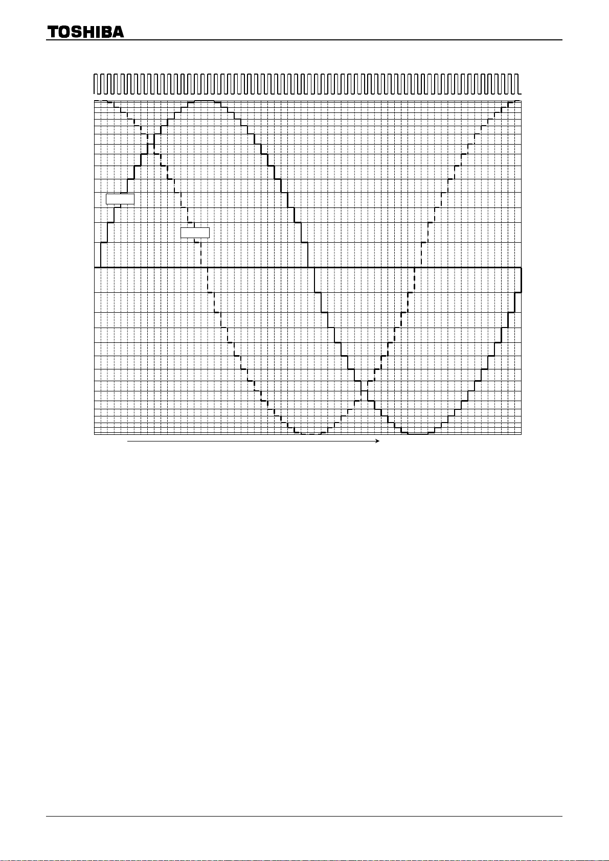
4-Bit Micro Step Output Current Vector Locus
X = 16
100
98
96
92
88
83
77
71
63
56
47
IA (%)
38
X = 15
X = 14
X = 13
X = 12
X = 11
CCW
(Normalizing each step to 90°°°°)
CW
X = 10
X = 9
X = 8
X = 7
X = 6
X = 5
X = 4
29
20
θX
10
0
10 20 29 38 47 56 63 71 77 83 88 92 96 98 100
θX
X = 3
X = 2
X = 1
X = 0
IB (%)
For input data, see the current function examples.
48
2001-09-05

Recommended Application Circuit
The values for the devices are all recommended values. For values under each input condition, see the
above-mentioned recommended operating conditions.
R
= 3.6 kΩ
osc
CR
C
= 560 pF
osc
V
DD
5 V
0 V
5 V
0 V
5 V
0 V
5 V
0 V
5 V
0 V
5 V
0 V
5 V
0 V
5 V
0 V
5 V
0 V
5 V
0 V
5 V
0 V
PGND
DATA MODE
CLK
ENABLE
CW/CCW
RESET
P-GND
DMODE 1
DMODE 2
DMODE 3
MDT 1
MDT 2
STANDBY
V
ref AB
V
R
RS A
R
RS B
V
SS
(FIN)
PROTECT
MO
M
A
A
B
B
SGND
OPEN
OPEN
TORQUE 1
TORQUE 2
DATA MODE
M
5 V
0 V
5 V
0 V
5 V
0 V
3 V
V
ref AB
R
0.66 Ω
RS A
STEPPING
MOTER
0.66 Ω R
RS B
TB62209F
1 µF
SGND
SGND
5 V
10 µF
Ccp 1
0.22 µF
SGND
Ccp C Ccp B Ccp A
Ccp 2
0.01 µF
100 µF
SGND
Note: Adding bypass capacitors is recommended.
Make sure that GND wiring has only one contact point, and to design the pattern that allows the heat
radiation.
To control setting pins in each mode by SW, make sure to pull down or pull up them to avoid high
impedance.
To input the data, see the section on the recommended input data.
Because there may be shorts between outputs, shorts to supply, or shorts to ground, be careful when
designing output lines, V
(VM) lines, and GND lines.
DD
24 V
49
2001-09-05

Package Dimensions
HSOP36-P-450-0.65 Unit: mm
TB62209F
Weight: g (typ.)
50
2001-09-05

TB62209F
RESTRICTIONS ON PRODUCT USE
• TOSHIBA is continually working to improve the quality and reliability of its products. Nevertheless, semiconductor
devices in general can malfunction or fail due to their inherent electrical sensitivity and vulnerability to physical
stress. It is the responsibility of the buyer, when utilizing TOSHIBA products, to comply with the standards of
safety in making a safe design for the entire system, and to avoid situations in which a malfunction or failure of
such TOSHIBA products could cause loss of human life, bodily injury or damage to property.
In developing your designs, please ensure that TOSHIBA products are used within specified operating ranges as
set forth in the most recent TOSHIBA products specifications. Also, please keep in mind the precautions and
conditions set forth in the “Handling Guide for Semiconductor Devices,” or “TOSHIBA Semiconductor Reliability
Handbook” etc..
• The TOSHIBA products listed in this document are intended for usage in general electronics applications
(computer, personal equipment, office equipment, measuring equipment, industrial robotics, domestic appliances,
etc.). These TOSHIBA products are neither intended nor warranted for usage in equipment that requires
extraordinarily high quality and/or reliability or a malfunction or failure of which may cause loss of human life or
bodily injury (“Unintended Usage”). Unintended Usage include atomic energy control instruments, airplane or
spaceship instruments, transportation instruments, traffic signal instruments, combustion control instruments,
medical instruments, all types of safety devices, etc.. Unintended Usage of TOSHIBA products listed in this
document shall be made at the customer’s own risk.
• The products described in this document are subject to the foreign exchange and foreign trade laws.
• The information contained herein is presented only as a guide for the applications of our products. No
responsibility is assumed by TOSHIBA CORPORATION for any infringements of intellectual property or other
rights of the third parties which may result from its use. No license is granted by implication or otherwise under
any intellectual property or other rights of TOSHIBA CORPORATION or others.
000707EBA
• The information contained herein is subject to change without notice.
51
2001-09-05
 Loading...