TB62201AFG
TOSHIBA Bi-CMOS Processor IC Silicon Monolithic
TB62201AFG
Dual-Stepping Motor Driver IC for OA Equipment Using PWM Chopper Type
The TB62201AFG is a dual-stepping motor driver driven by
chopper micro-step pseudo sine wave.
To drive two-phase stepping motors, Two pairs of 16-bit latch and
shift registers are built in the IC. The IC is optimal for driving
stepping motors at high efficiency and with low-torque ripple.
The IC supports Mixed Decay mode for switching the attenuation
ratio at chopping. The switching time for the attenuation ratio
can be switched in four stages according to the load.
Features
z Two stepping motors driven by micro-step pseudo sine wave
are controlled by a single driver IC
z Monolithic Bi-CMOS IC
z Low ON-resistance of Ron = 0.5 Ω (T
z ESD protection Exceeds 2000 V, MIL-STD-883D
z Two pairs of built-in 16-bit shift and latch registers
z Two pairs of built-in 4-bit DA converters for micro steps
z Built-in ISD, TSD, V
z Built-in charge pump circuit (two external capacitors)
z 36-pin power flat package (HSOP36-P-450-0.65)
z Output voltage: 40 V max
z Output current: 1.5 A/phase max
z Built-in Mixed Decay mode enables specification of four-stage attenuation ratio.
(The attenuation ratio table can be overwritten externally.)
z Chopping frequency can be set by external resistors and capacitors. High-speed chopping possible at 100 kHz or
higher.
DD&VM
power monitor (reset) circuit for protection
= 25°C @ 1.0 A: typ.)
j
Weight: 0.79 g (typ.)
Note: When using the IC, pay attention to thermal conditions.
These devices are easy damage by high static voltage.
In regards to this, please handle with care.
1
2005-04-04
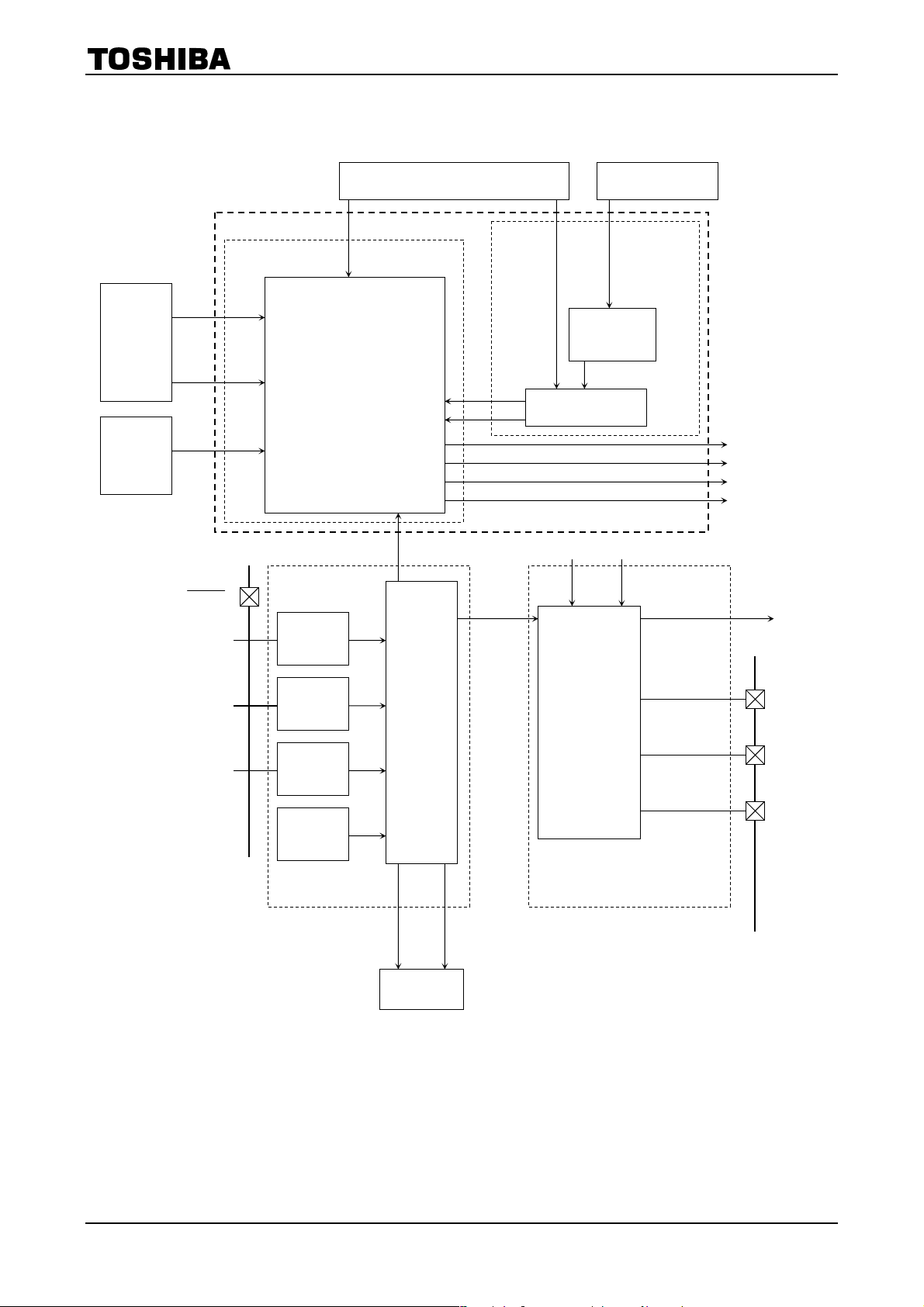
Block Diagram
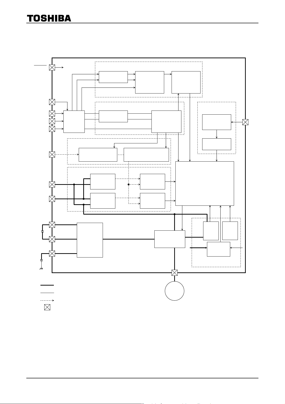
1. Overview (Power lines: A/B unit (C/D unit is the same as A/B unit))
TB62201AFG
RESET
SETUP
DATA
CLK
STROBE
V
R
V
ref
Mixed decay timing, table logic circuit
DATA
input
selector
Current Setting
Torque
control
16-bit shift
register
Current control data logic circuit
16-bit shift
register
(angle control)
16-bit latch
4-bit D/A
16-bit latch
Mixed decay
timing table
selector
Chopping reference
circuit
Chopping
waveform
generator
circuit
Waveform
shaping
circuit
CR
Current feedback circuit
S
M
V
RS
circuit 1
V
RS
circuit 2
RS COMP
circuit 1
Output control circuit
RS COMP
circuit 2
cp2
C
cp1
C
Charge
pump
circuit
High-Voltage Wiring (VM)
Logic data
Analog data
IC Terminal
Output circuit
(H-bridge)
Stepping
motor
Out X
circuit
V
M
Protected circuit
ISD
V
DDR/VMR
circuit
TSD
circuit
V
DD
2
2005-04-04
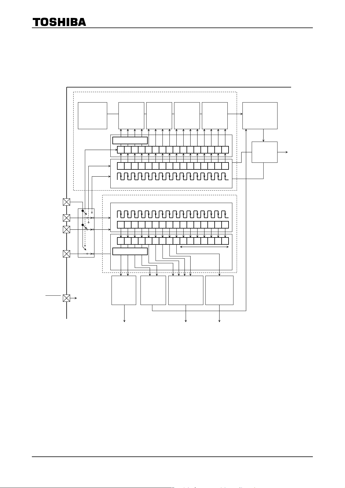
2. Logic Unit A/B (C/D unit is the same as A/B unit)
Function
This circuit is used to input from the DATA pins micro-step current setting data and to transfer them to the
subsequent stage. By switching the SETUP pin, the data in the mixed decay timing table can be
overwritten.
Mixed decay timing table logic circuit
TB62201AFG
SETUP
DATA
CLK
STROBE
Initial
setup
circuit
Data input
selector
Mixed
decay
timing
table 1
16-bit latch
0 1 2 3 4 5 6 7 8 9 10 11 12 13 14 15
0 1 2 3 4 5 6 7 8 9 10 11 12 13 14 15
16-bit shift register
Micro-step current setting data logic circuit
16-bit shift register
0 1 2 3 4 5 6 7 8 9 10 11 12 13 14 15
0 1 2 3 4 5 6 7 8 9 10 11 12 13 14 15
16-bit latch
Mixed
decay
timing
table 2
Mixed
decay
timing
table 3
Mixed
decay
timing
table 4
A unit side
Mixed
decay
timing
table selector
Mixed
decay
timing
Output
control
circuit
Torque
× 2 bits
RESET
Current feedback circuit D/A circuit
Decay
× 2 bits
B unit side
Current
× 4 bits
B unit side
Output control circuit
Note: The RESET and SETUP pins are pulled down in the IC by 10 kΩ resistor.
When not using these pins, connect them to GND. Otherwise, malfunction may occur.
Phase
× 1 bit
B unit side
3
2005-04-04
TB62201AFG
ng
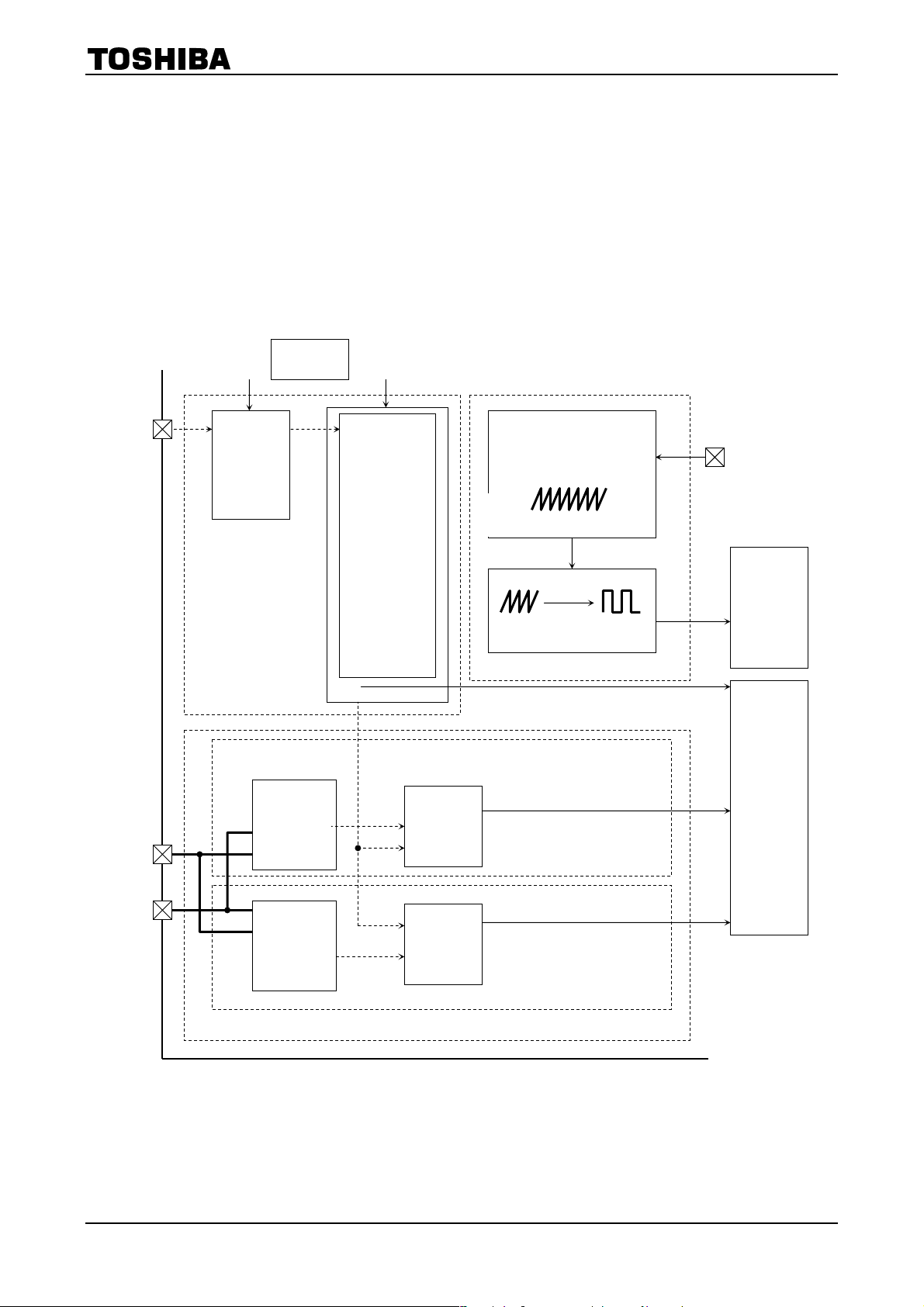
3. Current Feedback Circuit and Current Setting Circuit
(A/B unit (C/D unit is the same as A/B unit))
Function
The current setting circuit is used to set the reference voltage of the output current using the micro-step
current setting data input from the DATA pins.
The current feedback circuit is used to output to the output control circuit the relation between the set
current value and output current. This is done by comparing the reference voltage output to the current
setting circuit with the potential difference generated when current flows through the current sense
resistor connected between RS and V
The chopping waveform generator circuit to which CR is connected is used to generate clock used as
reference for the chopping frequency.
.
M
TORQUE
0, 1
V
ref
R
S
100%
85%
70%
50%
TORQUE
control
circuit
Current setting circuit
Logic
V
circuit 1
RS
(detects
potential
difference
between
RS and VM)
unit
CURRENT
15
14
13
12
11
10
9
8
7
6
5
4
3
2
1
0
0 to 3
Micro-step
current
setting
selector
circuit
4-bit
D/A
circuit
RS COMP
circuit 1
(Note 1)
m
or
circuit
generat
wavefor
Waveform shaping circuit
Chopping reference circuit
Output stop signal (ALL OFF)
Use in Charge mode
NF
(set current
reached signal)
CR
Mixed
decay
timing
circuit
Output
control
circuit
VM
Current feedback circuit
V
circuit 2
RS
(detects
potential
difference
between
VM and RS)
RS COMP
circuit 2
(Note 2)
RNF
(set current
monitor signal)
Use in Fast mode
Note 1: RS COMP 1: Compares the set current with the output current and outputs a signal when the output current
reaches the set current.
Note 2: RS COMP 2: Compares the set current with the output current at the end of Fast mode during chopping.
Outputs a signal when the set current is below the output current.
4
2005-04-04
TB62201AFG
y
4. Output Control Circuit, Current Feedback Circuit and Current Setting Circuit
(A/B unit (C/D unit is the same as A/B unit))
Micro-step current setting
Output control circuit Phase
Current
feedback
circuit
Current
setting
circuit
RESET
Output pin
V
M
NF
set current
reached signal
RNF
set current
monitor signal
Output stop
signal
Output control circuit
ISD (current
charge start
shutdown)
circuit
VMR
circuit
data logic circuit
Mixed
decay
timing
Output reset signal
Reset signal
selector
circuit
Chopping
reference circuit
Decay
mode
counter
CR counter
U
1
U
2
L
1
L
2
V
DD
Charge
pump
halt
signal
Charge pump
circuit
CR
VM
Mixed
decay
timing
circuit
Power suppl
for upper
output MOS
transistors
V
H
Output
circuit
Output
circuit
Ccp A
V
V
DD
DDR
circuit
Thermal
shut down
(TSD)
circuit
Protection circuit
Micro-step
current
setup latch clear
signal
Logic
Note: The RESET pins is pulled down in the IC by 10-kΩ resistor.
When not using the pin, connect it to GND. Otherwise, malfunction may occur.
Mixed decay
timing table
clear signal
Charge pump
circuit
V
: VDD power on Reset
DDR
VMR: VM power on Reset
ISD: Current shutdown circuit
TSD: Thermal shutdown circuit
Ccp B
Ccp C
5
2005-04-04
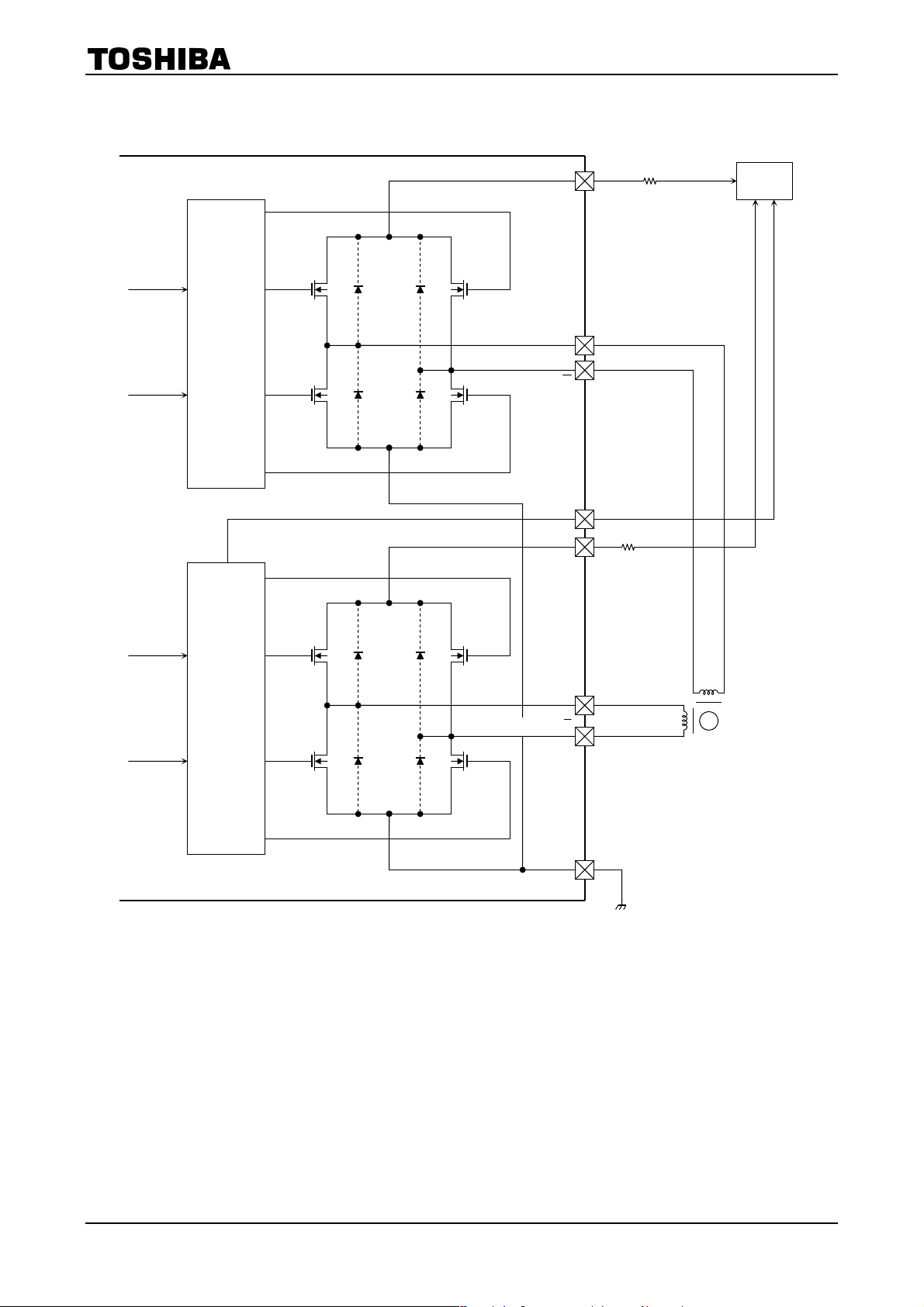
5. Output Equivalent Circuit (A/B unit (C/D unit is the same as A/B unit))
R
From
output
control
circuit
Output driver
circuit
U
1
U
2
L
1
L2
Power supply
for upper
output MOS
transistors
(VH)
Phase A
U1
L
S A
U
2
Output A
1
L2
Output
A
R
RS A
V
M B
TB62201AFG
To V
M
R
From
output
control
circuit
Output driver
circuit
U
1
U
2
L
1
L2
Power supply
for upper
output MOS
transistors
(VH)
Phase B
U1
L
S B
U
2
Output B
Output B
1
L2
R
RS B
PGND
M
6
2005-04-04
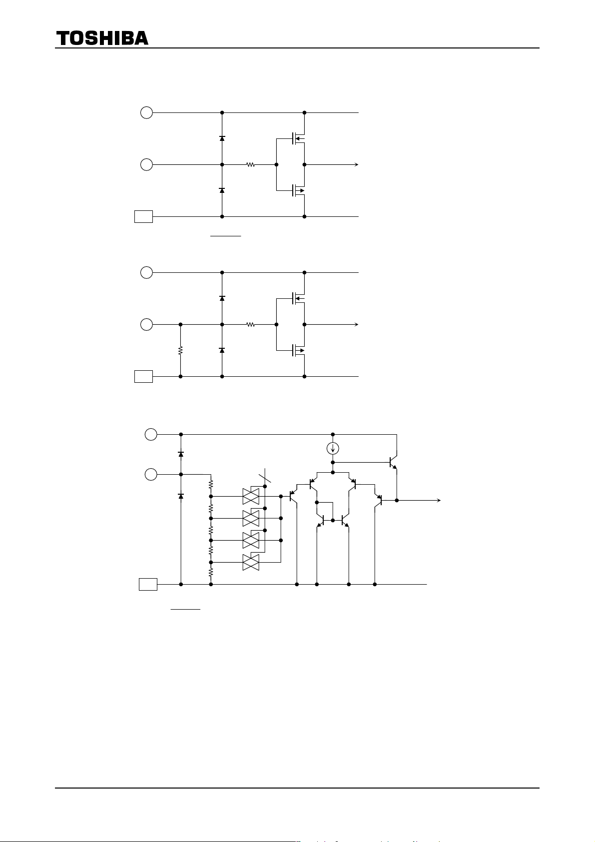
6. Input Equivalent Circuit
(1) Logic input circuit (CLK, DATA, STROBE)
VDD
27
IN
30/29/31
25/26/24
GND
FIN
(2) Input circuit (SETUP,
VDD
27
IN
6/28
RESET
TB62201AFG
To logic IC
150 Ω
)
To logic IC
150 Ω
GND
FIN
10 kΩ
(3) V
input circuit
ref
VDD
27
IN
9/10
GND
FIN
4
Note: The SETUP and RESET pins are pulled down. Do not use them open.
When not using these pins, connect them to GND.
To D/A circuit
7
2005-04-04
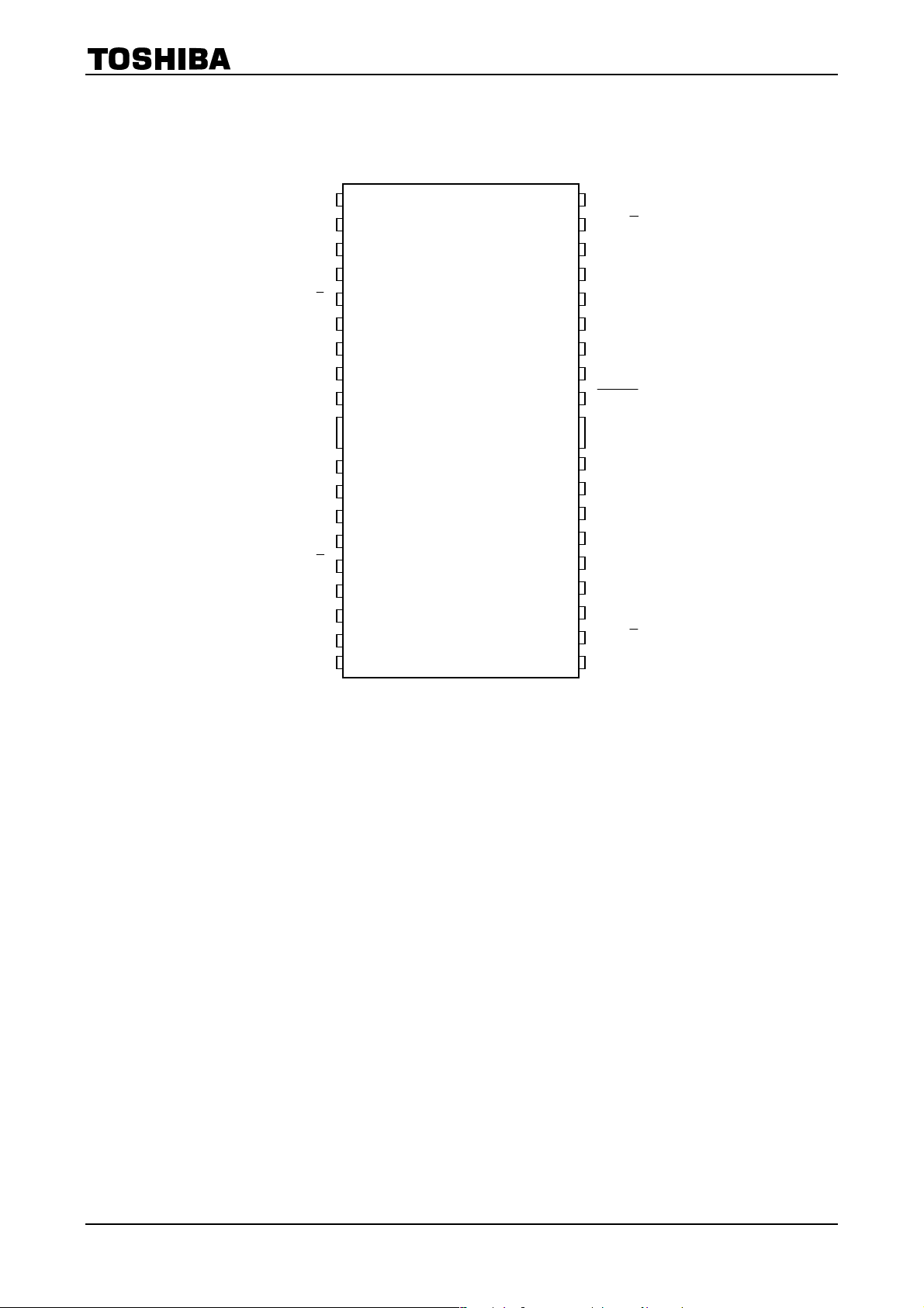
Pin Assignment
TB62201AFG
(Top view)
OUT B
OUT
SETUP
V
REF AB
V
SS
V
REF CD
OUT
OUT D
V
M B
R
S B
PGND
B
Ccp A
CR
(FIN)
NC
Ccp B
Ccp C
D
PGND
R
S D
V
MD
1
2
3
4
5
6
7
8
9
TB62201AFG
10
11
12
13
14
15
16
17
18
36
35
34
33
32
31
30
29
28
27
26
25
24
23
22
21
20
19
V
M A
OUT
A
R
S A
PGND
OUT A
STROBE AB
CLK AB
DATA AB
RESET
V
(FIN)
SS
V
DD
DATA CD
CLK CD
STROBE CD
OUT C
PGND
R
S C
C
OUT
V
MC
Note: [Important] If this IC is inserted reverse, voltages exceeding the voltages of standard may be applied to some
pins, causing damage.
Please confirm the pin assignment before mounting and using the IC.
8
2005-04-04

Pin Description
Pin No. Pin Symbol Description
TB62201AFG
1 V
2 OUT B Output B pin
3 R
4 PGND Power GND pin
5 B OUT Output B pin
6 SETUP CR setup switching pin (L: normal, H: setup)
7 Ccp A Capacitor pin for charge pump (Ccp1)
8 CR External C/R (osc) pin (sets chopping frequency)
9 V
FIN V
10 V
11 NC Non conection
12 Ccp B Capacitor pin for charge pump (Ccp2)
13 Ccp C Capacitor pin for charge pump (Ccp2)
14 D OUT Output D pin
15 PGND Power GND pin
16 R
17 OUT D Output D pin
18 V
19 V
20 C OUT Output C pin
21 R
22 PGND Power GND pin
23 OUT C Output C pin
24 STROBE CD CD STROBE (latch) signal input pin ( : LATCH)
25 CLK CD CD clock input pin
26 DATA CD CD serial data signal input pin
27 VDD Power pin for logic block
FIN V
28 RESET Output reset signal input pin (L: RESET)
29 DATA AB AB serial data signal input pin
30 CLK AB AB clock input pin
31 STROBE AB AB STROBE (latch) signal input pin ( : LATCH)
32 OUT A Output A pin
33 PGND Power GND pin
34 R
35 A OUT Output A pin
36 V
Voltage major for output B block
M B
Channel B current pin
S B
V
REF AB
FIN (VSS): Logic GND pin
SS
Vref input pin CD
REF CD
Channel D current pin
S D
Voltage major for output D block
M D
Voltage major for output C block
M C
Channel C current pin
S C
FIN (VSS) : Logic GND pin
SS
Channel A current pin
S A
Voltage major for output A block
M A
input pin AB
ref
Note: How to handle GND pins
All power GND pins and FIN (V
Since FIN also functions as a heat sink, take the heat dissipation into consideration when designing the board.
: signal GND) pins must be grounded.
SS
9
2005-04-04
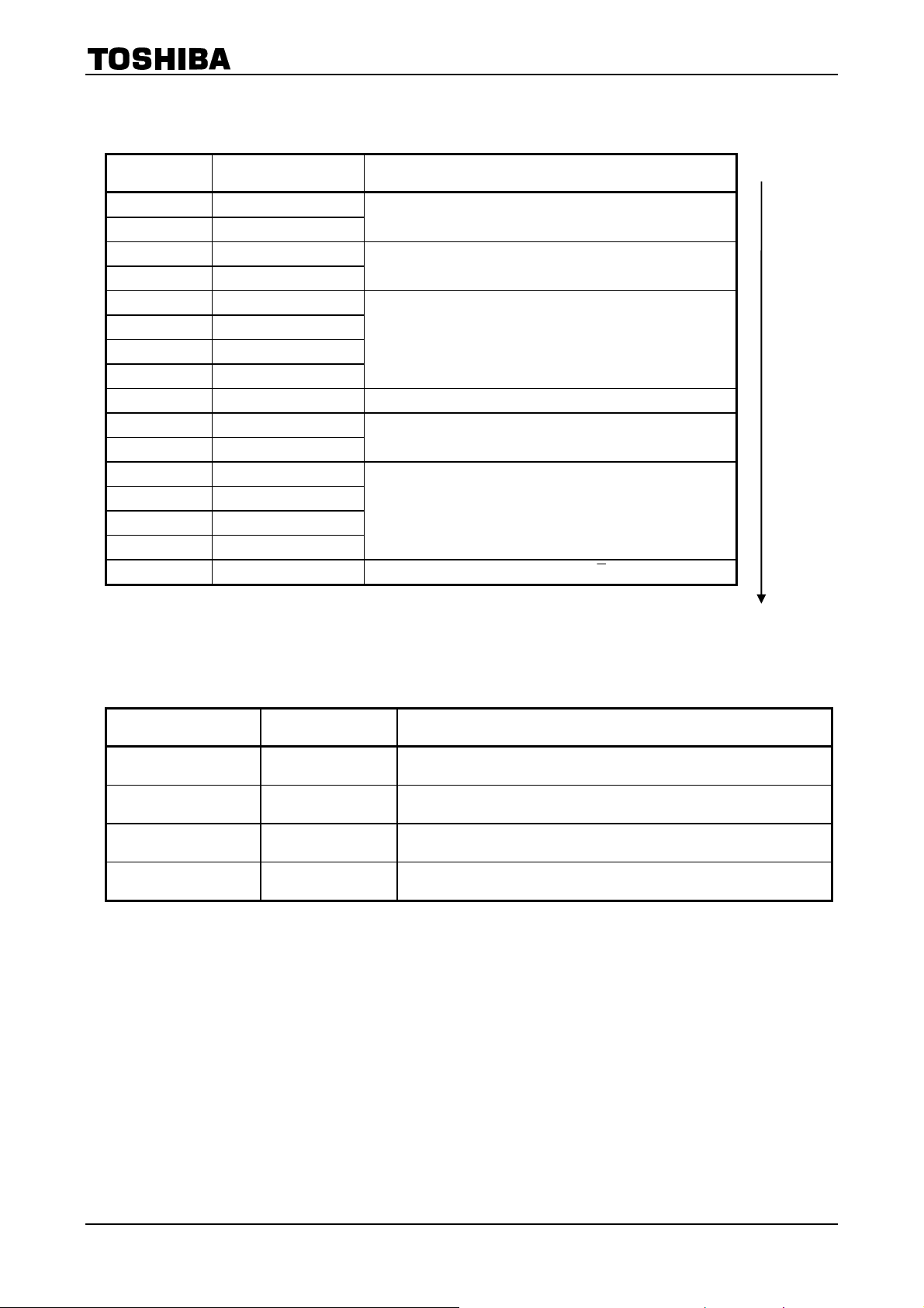
Signal Functions
TB62201AFG
1. Serial Input Signals
Data No. Name Functions
0 LSB TORQUE 0
1 TORQUE 1
2 DECAY MODE B0
3 DECAY MODE B1
4 Current B0
5 Current B1
6 Current B2
7 Current B3
8 PHASE B Phase information (H: OUT A: H, OUT A: L)
9 DECAY MODE A0
10 DECAY MODE A1
11 Current A0
12 Current A1
13 Current A2
14 Current A3
15 MSB PHASE A Phase information (H: OUT A: H, OUT A: L)
(for A/B. C/D is the same as A/B)
DATA No.0, 1
HL: 70%, LL: 50%
00: DECAY MODE 0, 01: DECAY MODE 1
10: DECAY MODE 2, 11: DECAY MODE 3
Used for setting current.
(LLLL
4-bit current B data
(Steps can be divided into 16 by 4-bit data)
00: DECAY MODE 0, 01: DECAY MODE 1
10: DECAY MODE 2, 11: DECAY MODE 3
Used for setting current.
(LLLL
4-bit current A data
(Steps can be divided into 16 by 4-bit data)
= HH: 100%, LH: 85%
= Output ALL OFF MODE)
= Output ALL OFF MODE)
(Note 1)
Note 1: Serial data input order
Serial data are input in the order LSB (DATA 0)
→ MSB (DATA 15)
Role of Data
Data Name Number of Bits Functions
TORQUE 2
DECAY MODE 2 × 2 phases
CURRENT 4 × 2 phases
PHASE 1 × 2 phases
Roughly regulates the current (four stages).
Common to A and B units.
Selects Decay mode.
A and B units are set separately.
Sets a 4−bit micro−step electrical angle.
A and B units are set separately.
Determines polarity (
A and B units are set separately.
+ or −).
10
2005-04-04
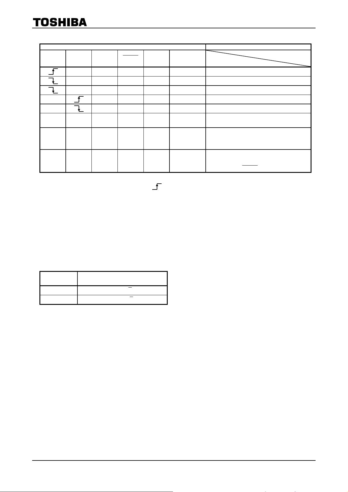
2. Serial Input Signal Functions
Input Action
CLK STROBE DATA RESET
× × H H L
× H H H L
× L H H L
× × H H L
× × H H L
× × × L × L
× × × × L L
× × × H H H
×: Don’t Care
Qn: Latched output level when STROBE is .
Note 1: V
DDR
and VMR
H when the operable range (3 V typical) or higher and L when lower.
When one of V
or VMR is operating, the system resets (OR relationship).
DDR
Note 2: High when TSD is in operation.
When one of TSD or ISD is operating, the system resets (OR relationship).
Note: Function of overcurrent protection circuit
Until the RESET signal is input after ISD is triggered, the overcurrent protection circuit remains in operation.
During ISD, the charge pump stays halted.
When TSD and ISD are operating, the charge pump halts.
3. PHASE Functions
VDDR
(Note 2) or
V
MR
Operation of
TSD/ISD
TB62201AFG
(Note 2)
No change in shift register.
H level is input to shift register.
L level is input to shift register.
Shift register data are latched.
Qn
Output off, charge pump halted
(S/R DATA CLR)
Output off (S/R DATA CLR)
Charge pump halted
Mixed decay timing table cleared (only V
Output off (S/R DATA HOLD)
Charge pump halted
Restored when
RESET goes from Low to High
DDR
)
Input Function
H Positive polarity (A: H, Α : L)
L Negative polarity (A: L, Α : H)
11
2005-04-04
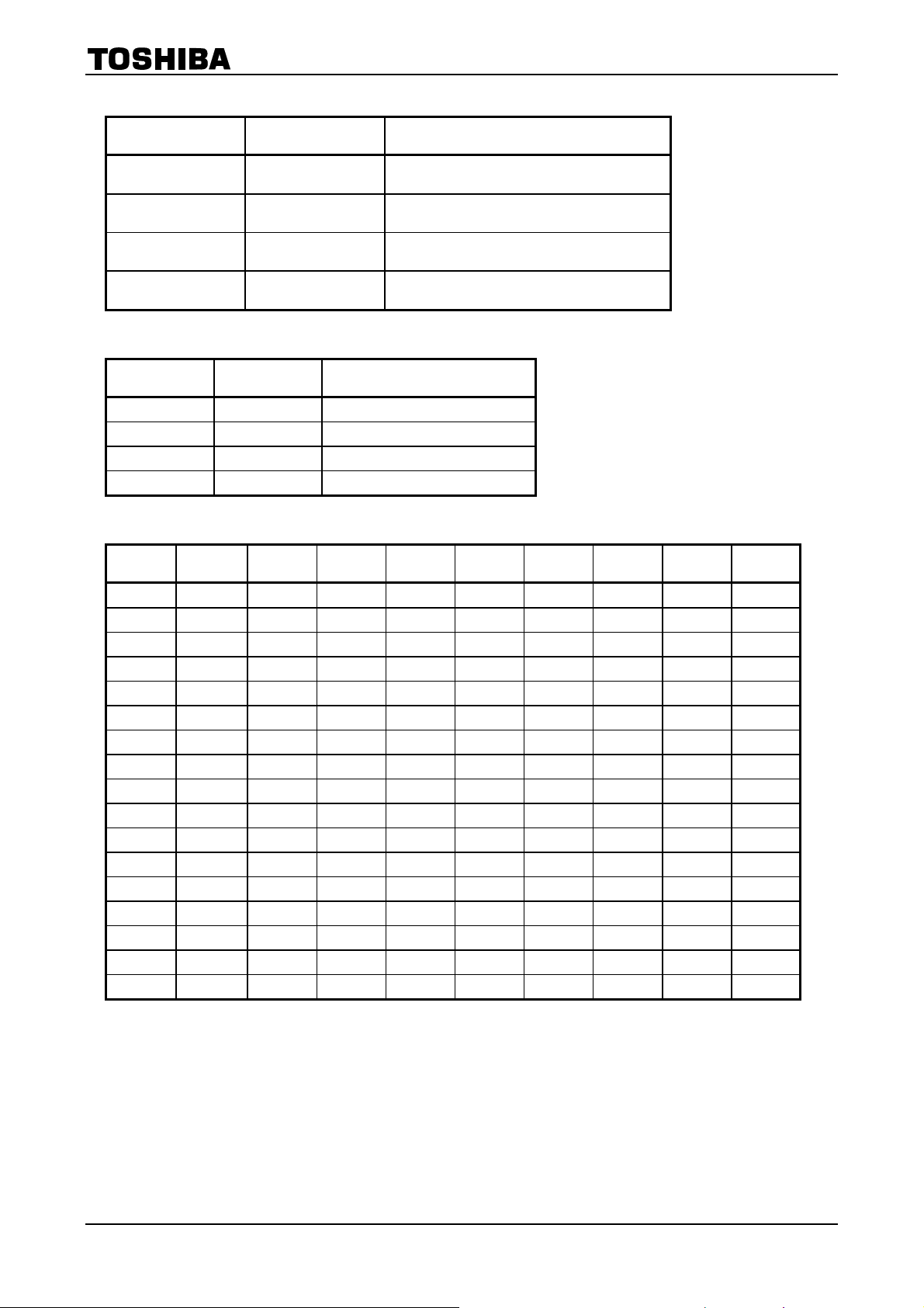
4. DECAY Mode X0, X1 Functions
DECAY MODE X1 DECAY MODE X0 Function
TB62201AFG
L L
L H
H L
H H
Decay mode 0
(Initial value: SLOW DECAY MODE)
Decay mode 1
(Initial value: MIXED DECAY MODE: 37.5%)
Decay mode 2
(Initial value: MIXED DECAY MODE: 75%)
Decay mode 3
(Initial value: FAST DECAY MODE)
5. TORQUE Functions
TORQUE 0 TORQUE 1 Comparator Reference Voltage Ratio
H H 100%
L H 85%
H L 70%
L L 50%
6. Current AX (BX) Functions
Step
16 90.0 H H H H L L L L
15 84.4 H H H H L L L H
14 78.8 H H H L L L H L
13 73.1 H H L H L L H H
12 67.5 H H L L L H L L
11 61.2 H L H H L H L H
10 56.3 H L H L L H H L
9 50.6 H L L H L H H H
8 45.0 H L L L H L L L
7 39.4 L H H H H L L H
6 33.8 L H H L H L H L
5 28.1 L H L H H L H H
4 22.5 L H L L H H L L
3 16.9 L L H H H H L H
2 11.3 L L H L H H H L
1 5.6 L L L H H H H H
0 0.0 L L L L H H H H
Set Angle
A3 A
A
2
A
1
By inputting the above current data (A: 4-bit, B: 4-bit), 17-microstep drive is possible. For 1 step fixed to 90
degrees, see the section on output current vector line (83 page).
B
0
B
3
B
2
B
1
0
12
2005-04-04
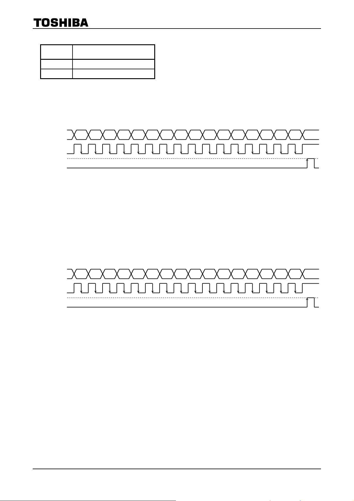
TB62201AFG
7. SETUP Functions
Input Function
H Decay timing data input mode
L Normal operating mode
Note: The SETUP pin is pulled down in the IC by 10-kΩ resistor.
8. Serial Data Input Setting
SETUP pin: L
DATA 0 1 2 3 4 5 6 7 8 9 10 11 12 13 14 15
CLK
STROBE
Note: Data input to the DATA pin are 16-bit serial data.
Data are transferred from DATA 0 (Torque 0) to DATA 15 (Phase A). Data are input and transferred at the
following timings.
At CLK falling edge: data input
At CLK rising edge: data transfer
After data are transferred, all data are latched on the rising edge of the STROBE signal.
As long as STROBE is not rising, the signal can be either Low or High during data transfer.
9. Serial Data Input Setting
(Normal operation)
(Decay timing setup)
SETUP pin: H
DATA 0 1 2 3 4 5 6 7 8 9 10 11 12 13 14 15
CLK
STROBE
Note: Data input to the DATA pin are 16-bit serial data.
• Data are transferred from DATA 0 (Current Mode 1) to DATA 15 (DECAY MODE X-4). Data are input and
transferred at the following timings.
• At CLK falling edge: data input
• At CLK rising edge: data transfer
• After data are transferred, all data are latched on the rising edge of the STROBE signal.
As long as STROBE is not rising, the signal can be either Low or High during data transfer.
13
2005-04-04

TB62201AFG
10. Conditions on Overwriting MIXED DECAY TIMING Table
If the following conditions are satisfied, the table can be overwritten.
• When
• When an internal reset is not triggered.
11. Data Input Signal at Setting Mixed Decay Timing Table
Data No. Name Function Initial Value
15 MSB Current Mode 3 Selects Slow or Mixed Decay mode 1 : MIXED DECAY MODE
14 DECAY MODE 3-2 Sets decay 3 ratio (decay 3 raito) 1
13 DECAY MODE 3-1 ↑ 1
12 DECAY MODE 3-0 ↑↑ 1 : 100% : FAST DECAY MODE
11 Current Mode 2 Selects Slow or Mixed Decay mode 1 : MIXED DECAY MODE
10 DECAY MODE 2-2 Sets decay 2 ratio 1
RESET = H (when RESET = L, the shift register is cleared, thus data cannot be input)
1) When the temperature is such that TSD is not triggered (or not reset by TSD).
2) Under a condition where ISD is not triggered (or not reset by ISD).
3) Both V
and VM are within the operating voltage.
DD
Note 1: While the output transistors are operating, do not rewrite the values in the mixed decay timing
table.
Note 2: The SETUP pins is pulled down in the IC by 10-kΩ resistor
When not using the pin, connect it to GND. Otherwise, malfunction may occur.
9 DECAY MODE 2-1 ↑ 0
8 DECAY MODE 2-0 ↑ 1 : 75% MIXED DECAY
7 Current Mode 1 Selects Slow or Mixed Decay mode 1 : MIXED DECAY MODE
6 DECAY MODE 1-2 Sets decay 1 ratio 0
5 DECAY MODE 1-1 ↑ 1
4 DECAY MODE 1-0 ↑ 0 : 37.5% MIXED DECAY
3 Current Mode 0 Selects Slow or Mixed Decay mode 0 : SLOW DECAY MODE
2 DECAY MODE 0-2 Sets decay 0 ratio 0
1 DECAY MODE 0-1 ↑ 0
0 LSB DECAY MODE 0-0 ↑ 0 (SLOW DECAY MODE)
Note 1: Input order of serial data
When setting decay timing, first input H to the SETUP pin, the same as for ordinary data, then
input data from LSB (DATA 0) to MSB (DATA 15).
When power is first turned on, the initial values in the table above are set as defaults.
Once latched, data are not cleared except by VDDR (power-on and power-off reset).
Next, after the mode changes to SETUP, the data are retained until mixed decay timing data are input and
latched.
14
2005-04-04

12. Function of Setting Mixed Decay Timing
CURRENT
MODE X
L Don’t care Don’t care Don’t care
H L L L 12.5%
H L L H 25.0%
H L H L 37.5%
H L H H 50.0%
H H L L 62.5%
H H L H 75.0%
H H H L 87.5%
H H H H
Mixed decay timing means the time for switching Slow mode to Fast mode in MIXED DECAY MODE.
In Mixed Decay mode, the Fast mode time at the end of chopping Cycle (T
The IC is switched from Slow to Fast mode according to the percentage representing mode time in the table
above.
(For example, 12.5% means that 12.5% of the time is in Fast mode and the rest of the time, 87.5%, in
Charge and Slow modes.)
Only when the value is maximum (100%), the mode is Fast Decay mode.
DECAY MODE
X-2
DECAY MODE
X-1
DECAY MODE
X-0
MIXED DECAY TIMING
(SLOW DECAY MODE)
(FAST DECAY MODE)
0%
100%
) is fixed by data.
chop
TB62201AFG
15
2005-04-04
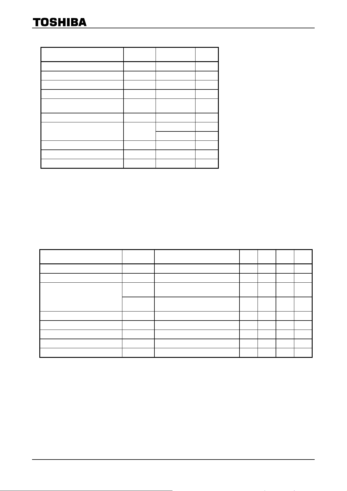
TB62201AFG
Maximum Ratings
Characteristics Symbol Rating Unit
Logic supply voltage VDD 7 V
Output voltage VM 40 V
Output current I
Current detect pin voltage VRS V
Charge pump pin maximum voltage
(CCP1 pin)
Logic input voltage VIN to VDD + 0.4 V
Power dissipation PD
Operating temperature T
Storage temperature T
Junction temperature Tj 150 °C
(Ta = 25°C)
1.5 A/phase (Note 1)
OUT
± 4.5 V
M
V
V
H
−40 to 85 °C
opr
−50 to 150 °C
stg
+ 7.0 V
M
1.4 W (Note 2)
3.2 W (Note 3)
Note 1: Perform thermal calculations for the maximum current value under normal conditions. Use the IC at 1.2 A or
less per phase.
Note 2: Input 7 V or less as V
.
IN
Note 3: Measured for the IC only. (Ta = 25°C)
Note 4: Measured when mounted on the board. (Ta = 25°C)
Ta: IC ambient temperature
T
: IC ambient temperature when starting operation
opr
T
: IC chip temperature during operation Tj (max) is controlled by TSD (thermal shut down circuit)
j
Recommended Operating Conditions
(Ta = 0 to 85°C)
Characteristics Symbol Test Condition Min Typ. Max Unit
Power supply voltage VDD ⎯ 4.5 5.0 5.5 V
Output voltage VM VDD = 5.0 V 20 24 34 V
= 25°C, per phase
I
OUT (1)
Output current
I
OUT (2)
Logic input voltage VIN ⎯ GND ⎯ VDDV
Clock frequency f
Chopping frequency f
Reference voltage V
Current detect pin voltage VRS VDD = 5.0 V 0 ±1.0 ±1.5 V
CLK
chop
ref
Ta
(when one motor is driven)
= 25°C, per phase
Ta
(when two motors are driven)
VDD = 5.0 V 1.0 6.25 25 MHz
VDD = 5.0 V 40 100 150 kHz
VM = 24 V, T
= 100% 2.0 3.0 V
orque
⎯ 1.1 1.3 A
⎯ 1.1 1.3 A
DD
Note: Use the Maximum Junction Temperature (Tj) at 120°C or less
V
16
2005-04-04

Electrical Characteristics 1
(unless otherwise specified, Ta = 25°C, VDD = 5 V, VM = 24 V)
TB62201AFG
Characteristics Symbol
Input voltage
Input current 1
Input current 2
Power dissipation (VDD pin)
Power dissipation (VM pin)
High VIN
Low V
IN (L)
I
IN1 (H)
I
IN1 (L)
I
IN2 (H)
I
IN2 (L)
I
DD1
I
DD2
IM1
IM2
I
Test
Circuit
2.0 VDD
(H)
1 CLK,
⎯ ⎯ 1.0
⎯ ⎯ 700
CLK, STROBE, DATA pins
2
RESET , SETUP pins
V
DD
DATA
Logic, output all off
2
Output OPEN, f
LOGIC ACTIVE, V
Charge Pump
Output OPEN (STROBE,
DATA
Logic, output all off
Charge Pump
3
Output OPEN, f
LOGIC ACTIVE, V
V
M
Charge Pump
Output OPEN, f
LOGIC ACTIVE, 100 kHz
4
M3
chopping (emulation), Output OPEN,
Charge Pump
µF, Ccp2
Test Condition Min Typ. Max Unit
RESET , STROBE, DATA pins
GND
− 0.4
GND 0.8
⎯ ⎯ 1.0
⎯ ⎯ 700
= 5 V (STROBE, RESET ,
= L), RESET = L,
= 6.25 MHz
CLK
= 5 V,
DD
= charged
⎯ 3.0 6.0
⎯ 4.0 80
RESET ,
= L), RESET = L,
⎯ 5.0 6.0
= no operation
= 6.25 MHz
CLK
= 5 V,
= 24 V, Output off
DD
⎯ 12 20
= charged
= 6.25 MHz
CLK
⎯ 30 40
= charged Ccp1 = 0.22
= 0.01µf
V
DD
+ 0.4
V
µA
µA
mA
mA
Output standby
current
Upper I
OH
Output bias current Upper IOB
Output leakage
current
Comparator
Lower I
High
(reference)
Mid high V
OL
V
RS (H)
RS (MH)
reference voltage
ratio
Output current differential ∆I
Output current setting differential ∆I
Mid low V
Low V
RS (ML)
RS (L)
7
out1
7 I
out2
RS pin current IRS 8
V
= VM = 24 V, V
RS
out
= 0 V,
RESET = H, DATA = ALL L
V
= VM = 24 V, V
RS
5
RESET = H, DATA = ALL L
V
= VM = CcpA = V
RS
= 24 V,
out
out
RESET = L
6
= 3.0 V, V
V
ref
TORQUE
= 3.0 V, V
V
ref
TORQUE
= 3.0 V, V
V
ref
TORQUE
= 3.0 V, V
V
ref
TORQUE
(Gain) = 1/5.0
ref
= (H.H) = 100% set
(Gain) = 1/5.0
ref
= (H.L) = 85% set
(Gain) = 1/5.0
ref
= (L.H) = 70% set
(Gain) = 1/5.0
ref
= (L.L) = 50% set
Differences between output current
channels
I
= 1000 mA
out
= 1000 mA −5 ⎯ 5 %
out
= 24 V, V
VRS
(RESET status)
= 24 V, RESET = L
M
=24 V,
−400 ⎯ ⎯
−200 ⎯ ⎯
µA
⎯ ⎯ 1.0
⎯ 100 ⎯
83 85 87
%
68 70 72
48 50 52
−5 ⎯ 5 %
⎯ ⎯ 10 µA
17
2005-04-04

Characteristics Symbol
Output transistor drain-source
on-resistance
R
ON (D-S) 1
R
ON (D-S) 1
R
ON (D-S) 2
R
ON (D-S) 2
Test
Circuit
9
I
out
T
I
out
T
I
out
T
I
out
T
Test Condition Min Typ. Max Unit
= 1.0 A, V
= 25°C, Drain-Source
j
= 1.0 A, VDD = 5.0 V
= 25°C, Source-Drain
j
= 1.0 A, VDD = 5 V,
= 105°C, Drain-Source
j
= 1.0 A, VDD = 5 V,
= 105°C, Source-Drain
j
= 5.0 V
DD
Electrical Characteristics 2
(unless otherwise specified, Ta = 25°C, VDD = 5 V, VM = 24 V)
TB62201AFG
⎯ 0.5 0.6
⎯ 0.5 0.6
Ω
⎯ 0.6 0.75
⎯ 0.6 0.75
Characteristics Symbol
V
input voltage V
ref
V
input current I
ref
V
attenuation ratio V
ref
TSD temperature
TSD return temperature difference ∆TjTSD 11 TjTSD = 130 to 170°C ⎯
VDD return voltage V
VM return voltage VMR 13
Over current protected circuit
operation current
ref
ref
(GAIN) 6
ref
TSD
T
j
(Note 1)
DDR
ISD
(Note 2)
Test
Circuit
V
10
10
12
M
RESET = H, Output on
RESET = H, Output off
V
M
V
ref
V
M
RESET
V
ref
11 V
DD
V
M
STROBE
V
DD
STROBE
VDD = 5 V, VM = 24 V,
14
fchop
Test Condition Min Typ. Max Unit
= 24 V, VDD = 5 V,
= 24 V, VDD = 5 V,
= 3.0 V
= 24 V, VDD = 5 V,
= H, Output on,
= 2.0 to VDD − 1.0 V
= 5 V, VM = 24 V 130 ⎯ 170 °C
= 24 V, RESET = H,
= H
= 5 V,
= H
= 100 kHz set
RESET
= H,
Note 1: Thermal shut down (TSD) circuit
When the IC junction temperature reaches the specified value and the TSD circuit is activated, the internal
reset circuit is activated switching the outputs of both motors to off.
When the temperature is set between 130 (min) to 170°C (max), the TSD circuit operates. When the TSD
circuit is activated, the function data latched at that time are cleared. Output is halted until the reset is
released. While the TSD circuit is in operation, the charge pump is halted.
Even if the TSD circuit is activated and RESET goes H → L → H instantaneously, the IC is not reset until
the IC junction temperature drops 35°C (typ.) below the TSD operating temperature (hysteresis function).
Note 2: Overcurrent protection circuit
When current exceeding the specified value flows to the output, the internal reset circuit is activated
switching the outputs of both shafts to off.
When the ISD circuit is activated, the function data latched at that time are cleared.
Until the RESET signal is input, the overcurrent protection circuit remains activated.
During ISD, the charge pump halts.
For failsafe operation, be sure to add a fuse to the power supply.
2.0
0
1/4.8 1/ 5.0 1/5.2
2.0
2.0
⎯ 2.6 ⎯ A
⎯ V
⎯ 100 A
TSD
T
j
−35
⎯ 4.0 V
⎯ 4.0 V
DD
⎯ °C
V
⎯
18
2005-04-04
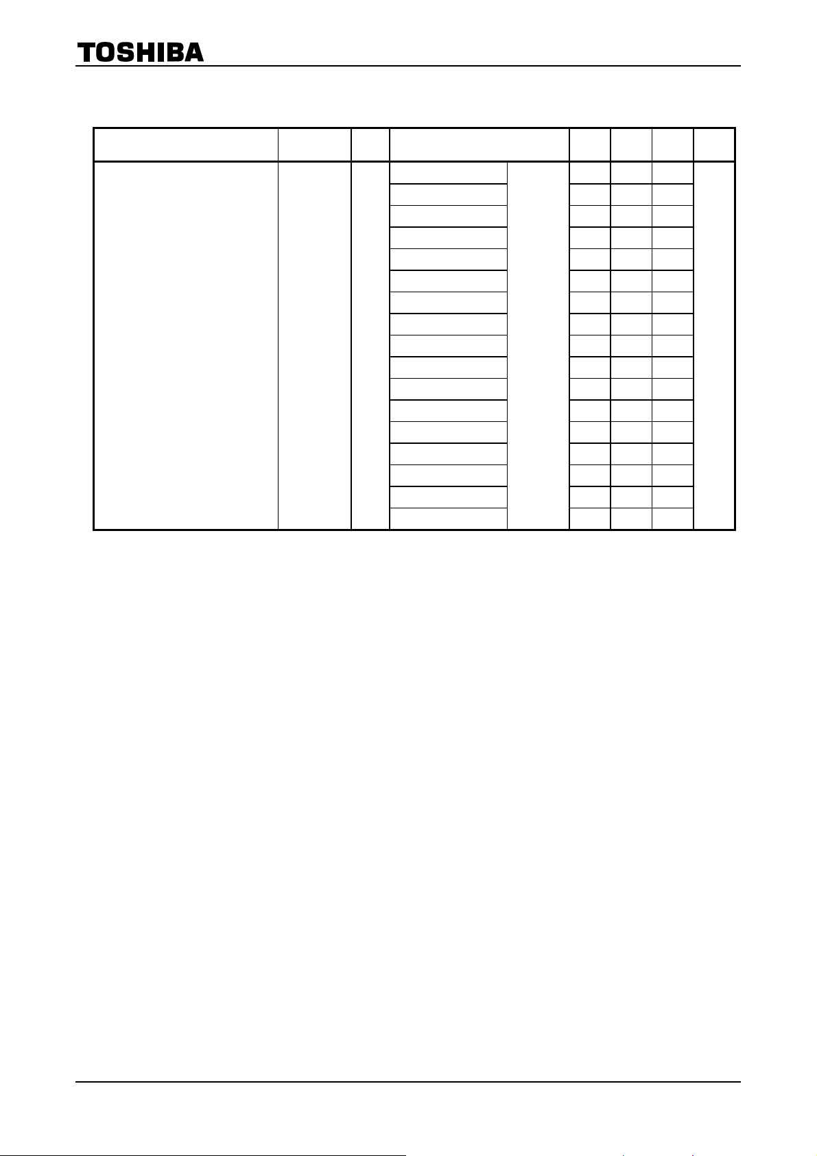
Electrical Characteristics 3
(Ta = 25°C, VDD = 5 V, VM = 24 V, I
= 1.0 A)
out
TB62201AFG
Characteristics Symbol
Chopper current Vector 15
Test
Circuit
θA = 90 (θ16) ⎯ 100 ⎯
θA = 84 (θ15) ⎯ 100 ⎯
θA = 79 (θ14) 93 98 ⎯
θA = 73 (θ13) 91 96 ⎯
θA = 68 (θ12) 87 92 97
θA = 62 (θ11) 83 88 93
θA = 56 (θ10) 78 83 88
θA = 51 (θ9) 72 77 82
θA = 45 (θ8) 66 71 76
θA = 40 (θ7) 58 63 68
θA = 34 (θ6) 51 56 61
θA = 28 (θ5) 42 47 52
θA = 23 (θ4) 33 38 43
θA = 17 (θ3) 24 29 34
θA = 11 (θ2) 15 20 25
θA = 6 (θ1) 5 10 15
θA = 0 (θ0)
Test Condition Min Typ. Max Unit
⎯
⎯ 0 ⎯
%
19
2005-04-04
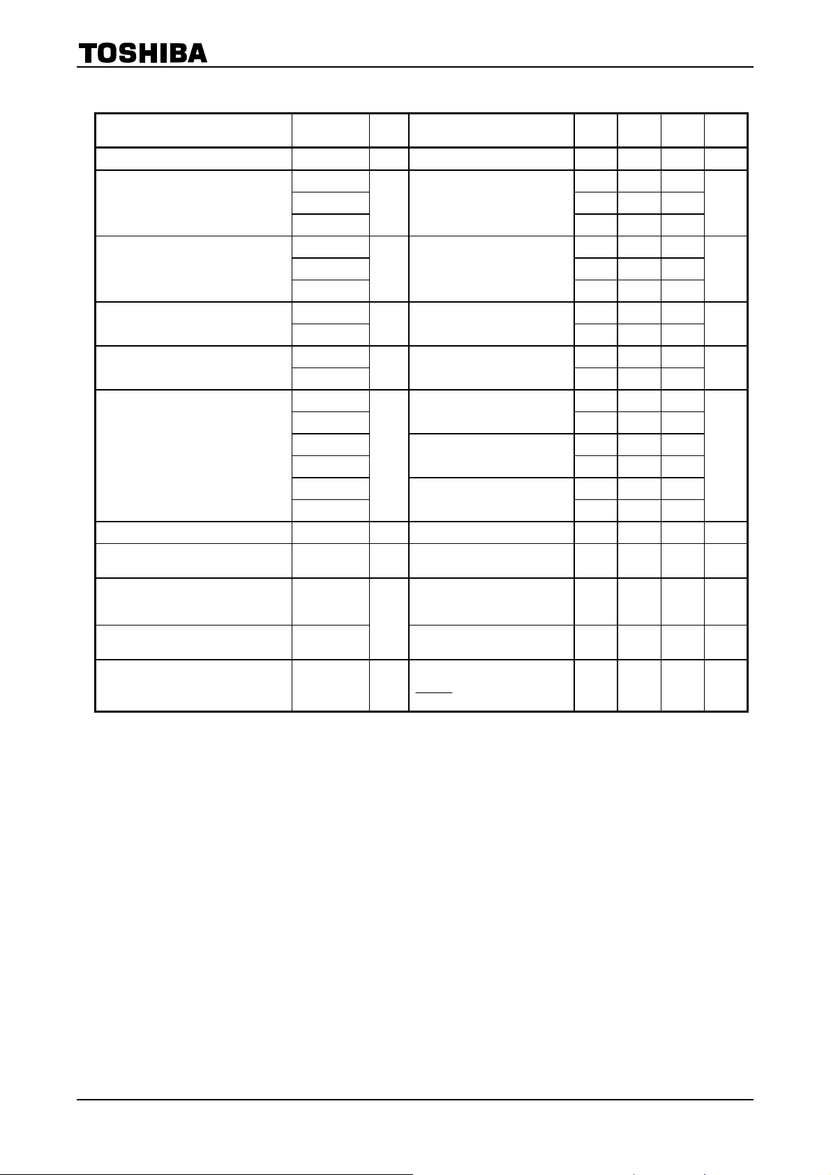
TB62201AFG
AC Characteristics
(Ta = 25°C, VM = 24 V, VDD = 5 V, 6.8 mH/5.7 Ω)
Characteristics Symbol
Clock frequency f
Minimum clock pulse width
Minimum STROBE pulse width
Data setup time
Data hold time
Output transistor switching
characteristic
Noise rejection dead band time t
CR reference signal oscillation
frequency
Chopping frequency range
Chopping frequency f
Charge pump rise time t
Test
Circuit
16 ⎯ 1.0 ⎯ 25 MHz
CLK
tw
40 ⎯ ⎯
(CLK)
twp
(CLK)
t
wn (CLK)
t
STROBE
t
STROBE (H)
t
STROBE (L)
t
suSIN-CLK
t
suST-CLK
t
Hsin-CLK
t
hCLK-ST
tr ⎯ 0.1 ⎯
16
20 ⎯ ⎯
40 ⎯ ⎯
16 ⎯
16
20 ⎯ ⎯
16
Output Load; 6.8 mH/5.7
tf
t
t
t
t
f
chop (min)
f
chop (typ.)
f
chop (max)
⎯ 15 ⎯
pLH (ST)
pHL (ST)
⎯ 1.2 ⎯
pLH (CR)
pHL (CR)
19 I
BLNK
f
20 C
CR
STROBE (↑) to VOUT
18
Output Load; 6.8 mH/5.7
CR to VOUT
Output Load; 6.8 mH/5.7
Output active (I
Step fixed, Ccp1
Ccp2
20
chop
Output active (I
CR CLK
Ccp2
21
ONG
V
Test Condition Min Typ. Max Unit
⎯
20
⎯ ⎯
20 ⎯ ⎯
20
⎯
20 ⎯ ⎯
20
⎯
20
Ω
Ω
Ω
= 1.0 A 200 300 400 ns
out
= 560 pF, R
osc
= 0.01 µF
= 800 kHz
= 0.22 µF, Ccp = 0.01 µF
= 24 V, VDD = 5 V,
M
= L → H
RESET
= 3.6 kΩ ⎯ 736 ⎯ kHz
osc
= 1.0 A)
out
= 0.22 µF,
= 1.0 A)
out
⎯ 0.1 ⎯
⎯ 10 ⎯
⎯ 2.5 ⎯
40 100 150 kHz
⎯ 100 ⎯ kHz
⎯ 2 4 ms
⎯ ⎯
⎯ ⎯
⎯ ⎯
ns
ns
ns
ns
µs
20
2005-04-04
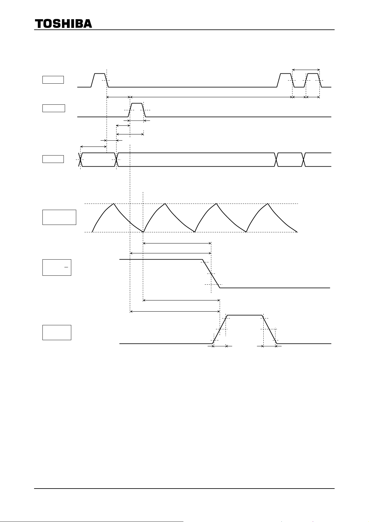
TB62201AFG
Test Waveforms
CLK
STROBE
t
suSIN-CLK
50%
DATA
CR waveform
(reference)
DATA15 DATA0
(Timing waveforms and names)
50%
t
suST-CLK
50%
t
hSIN-CLK
50%
t
STROBE (L)
t
STROBE
t
STROBE (H)
t
hCLK-ST
t
w (CLK)
twn t
wp
OUTPUT
Voltage A
Output
voltage
A
t
pHL (CR)
t
pHL (ST)
t
pLH (CR)
t
pLH (ST)
90%
50%
10%
t
r
10%
50%
90%
90%
50%
10%
tf
21
2005-04-04
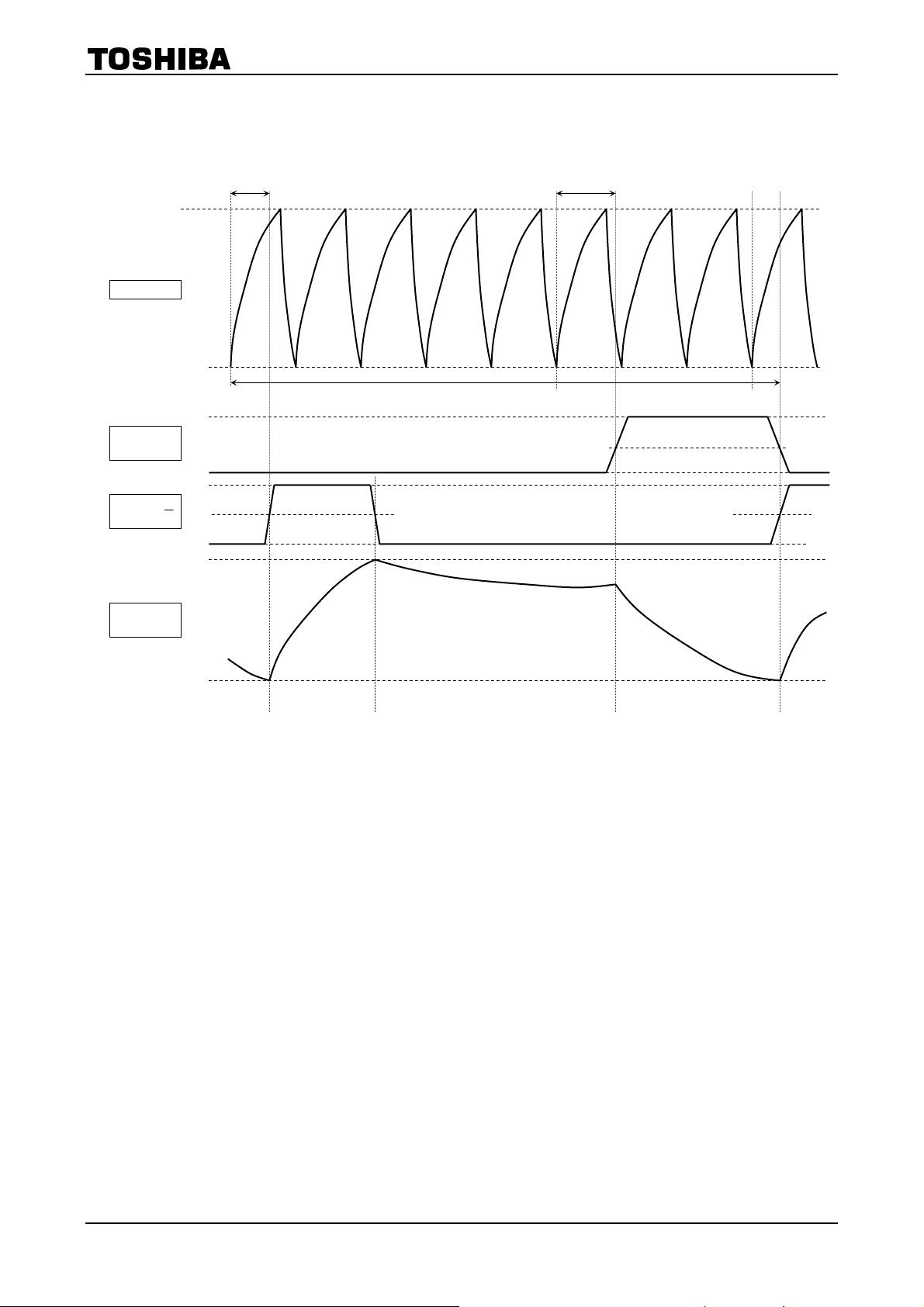
TB62201AFG
Test Waveforms
H
OSC (CR)
L
H
Output
voltage A
L
H
Output
voltage
A
L
Set current
(Timing waveforms and names)
OSC-charge delay
T chop
50%
OSC-fast delay
50%
50%
Output
current
L
Slow Charge
Fast
22
2005-04-04

Calculation of Set Current
TB62201AFG
Determining RRS and V
I
(max) =
out
1/5.0 is V
For example,
to input V
R
(gain): V
ref
RS
1
(GAIN) V
ref
= 0.75 Ω (0.5 W or more) is required.
determines the set current value.
ref
=
× V
(V) ×
ref
attenuation ratio (typ.).
ref
= 3 V and Torque = 100% and to output I
ref
orqueorque
R
RS
out
)( )Ω
= 0.8 A,
Formulas for Calculating CR Oscillation Frequency
The CR oscillation frequency and f
1
1
[Hz]
f
KA (constant): 0.523
KB (constant): 600
f
Example: When Cosc = 1,000 pF and Rosc = 2.0 kΩ are connected, f
At this time, the chopping frequency f
Note: fCR =
CR
chop
=
f
CR
=
8
t
CR
can be calculated by the following formulas:
chop
[Hz]
C)KBR(CKA
××××
CR
CR
chop
is: f
= fCR/8 = 92 kHz.
chop
+=
Charge)-(Dis t (Charge) t t
dataserial input :50% 70, 85, 100, (T T
(Chopping reference frequency)
= 735 kHz.
CR oscillation CR charge CR distance
cycle time time
At this time, t (CR − discharge) is subject to the following condition :
600 ns > t (CR − discharge) > 400 ns.
Be sure to set the CR value in accordance with this condition.
23
2005-04-04

TB62201AFG
CR Circuit Constants
OSC circuit oscillation waveform
t (CR
− charge) t (CR − dis-charge)
E1
E2
= 0 t = 1 t = 2
t
The OSC circuit generates the chopping reference signal by charging and discharging the external capacitor Cosc
through current supplied from the external resistor Rosc in the OSC block.
Voltages E1 and E2 in the diagram are set by dividing the V
The actual current chopping time is 1/8 the CR frequency.
[Important: Setting the cr circuit constants]
by approximately 3/5 (E1) and 2/5 (E2).
DD
The CR oscillation waveform is converted in the IC to the CLK waveform (CR-CLK signal) and used for control.
If the CR waveform discharge time is set outside the range shown below, the operation of the IC is not guaranteed.
Be sure to set the CR waveform discharge time within the following range.
600 ns > t (CR discharge) > 400 ns
24
2005-04-04

TB62201AFG
IC Power Dissipation
IC power dissipation is classified into two: power consumed by transistors in the output block and power consumed
by the logic block and the charge pump circuit.
(1) Power consumed by the Power Transistor (calculated with Ron = 0.6 Ω)
In Charge mode, Fast Decay mode, or Slow Decay mode, power is consumed by the upper and lower transistors
of the H bridges. The following expression expresses the power consumed by the transistors of a H bridge.
P (out) = 2 (T
The average power dissipation for output under 4−bit micro step operation (phase difference between phases A
and B is 90°) is determined by expression (1).
Thus, power dissipation for output per unit is determined as follows (2) under the conditions below.
R
= 0.6 Ω (@ 1.0 A)
on
I
(Peak: max) = 1.0 A
out
V
= 24 V
M
V
= 5 V
DD
P (out) = 2 (T
=1.20 (W)
) × I
r
r
(A) × VDS (V) = 2 × I
out
) × 1.0 (A)^2 × 0.60 (Ω) ................................................................. (2)
^2 × Ron......................................(1)
out
(2) Power consumed by the logic block and IM
The following standard values are used as power dissipation of the logic block and IM at operation.
I (LOGIC) = 2 mA (typ.): /unit
I (IM3) = 12.5 mA (typ.): operation/unit
I (IM1) = 6.0 mA (typ.): stop/unit
The logic block is connected to V
current consumed by output switching) is connected to V
P (Logic & IM) = 5 (V) × 0.002 (A) + 24 (V) × 0.0125 (A).................................... (3)
= 0.31 (W)
(5 V). IM (total of current consumed by the circuits connected to VM and
DD
(24 V). Power dissipation is calculated as follows :
M
(3) Thus, power dissipation for 1 unit (P) is determined as follows by (2) and (3) above.
P = P (out) + P (Logic & IM) = 1.51 (W)
Power dissipation for 1 unit at standby is determined as follows:
P (standby) = 24 (V) × 0.006 (A) + 5 (V) × 0.002 (A)
= 0.154 (W)
When one motor driving = 100 %, power dissipation is determined as follows:
P (all) = 1.51 (W) + 1.664 (W) = 1.66 (W)
For thermal design on the board, evaluate by mounting the IC.
25
2005-04-04
TB62201AFG
Mixed Decay Mode Waveforms
CR pin
input
waveform
DECAY MODE 0
SLOW
DECAY
MODE
37.5%
MIXED
DECAY
MODE
NF
Charge
NF
Charge
(concept of mixed decay mode)
f
chop
Set current value
Slow
Slow
MDT
Set current value DECAY MODE 1
Fast
Monitoring
set current
value
RNF
RNF
DECAY MODE 2
75%
MIXED
DECAY
MODE
DECAY MODE 3
FAST
DECAY
MODE
Charge
Charge
100% 75% 50% 25% 0
A B C D E F G H I
NF
Fast
MDT
NF
Fast
87.5% 62.5% 37.5% 12.5%
Set current value
Monitoring
set current
value
RNF
Set current value
Monitoring
set current
value
RNF
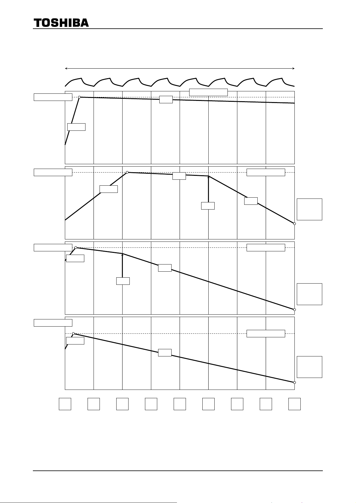
In Decay modes 1 to 4, any point from A to H can be set using 3-bit + 1-bit serial data × 4.
(Slow Decay mode for Decay mode 0 in the above figure can be set by setting current Decay mode X to 0.)
NF is the point where the output current reaches the set current value. RNF is the timing for monitoring the set
current.
In Mixed Decay and Fast Decay modes, where the condition RNF (set current monitor signal) < (output current)
applies, Charge mode is cancelled at the next chopping cycle (charge cancel circuit). Therefore, at the next chopping
cycle, the IC enters Slow + Fast modes (Slow → Fast at MDT).
26
2005-04-04

Mixed Decay Timing which can be Set
f
Internal
CR
waveform
NF
chop
TB62201AFG
Defaults for
Decay mode 0
0%
12.5%
25%
37.5%
50%
NF
NF
NF
NF
MDT
MDT
MDT
MDT
CURRENT MODE (X)
DECAY MODE (X
X: arbitrary value
CURRENT MODE (X)
DECAY MODE (X
RNF
CURRENT MODE (X)
DECAY MODE (X
RNF
Defaults for
Decay mode 1
CURRENT MODE (X)
DECAY MODE (X
RNF
CURRENT MODE (X)
DECAY MODE (X
= 0
− 2, X − 1, X − 0) = (×, ×, ×)
= 1
− 2, X − 1, X − 0) = (0, 0, 0)
= 1
− 2, X − 1, X − 0) = (0, 0, 1)
= 1
− 2, X − 1, X − 0) = (0, 1, 0)
= 1
− 2, X − 1, X − 0) = (0, 1, 1)
62.5%
75%
87.5%
FAST
DECAY
MODE
NF
NF
MDT
NF
MDT
NF
FAST MODE → RNF: CURRENT MONITOR →
(WHEN SET CURRENT VALUE > OUTPUT CURRENT)
CHARGE MODE → FAST MODE
MDT
RNF
CURRENT MODE (X)
DECAY MODE (X
RNF
Defaults for
Decay mode 2
CURRENT MODE (X)
DECAY MODE (X
RNF
CURRENT MODE (X)
DECAY MODE (X
RNF
Defaults for
Decay mode 3
CURRENT MODE (X)
DECAY MODE (X
RNF
= 1
− 2, X − 1, X − 0) = (1, 0, 0)
= 1
− 2, X − 1, X − 0) = (1, 0, 1)
= 1
− 2, X − 1, X − 0) = (1, 1, 0)
= 1
− 2, X − 1, X − 0) = (1, 1, 1)
27
2005-04-04
 Loading...