

查询TB6066FNG供应商
TOSHIBA BiCMOS Linear Integrated Circuit Silicon Monolithic
TB6066FNG
Shock Sensor IC
TB6066FNG detects an existence of external shock through the
shock sensor and output Low-level signal at 7 pin.
It has so excellent characteristic in S/N ratio that user can use
Analog signal for mechanical control systems, like servo control.
Features
• TB6066FNG operates from 2.7 to 5.5 V DC single power
supply voltage.
• Signal from the shock sensor is amplified according to setting
gain, and is detected through the internal window
comparator.
• Input terminal of sensor signal is designed high impedance.
Differential input impedance = 100 MΩ (typ.)
• Three Operatinal-Amplifier is built in for design flexibility. (*Note 1)
• Sensitivity of shock detection can be adjusted by external devices.
• Small package: SSOP16-P-225-0.65B (0.65 mm pitch)
• Excellent S/N ratio: Improved 10dB compared with our TA6038FN/FNG
*Note 1: LPF (low pass filter) circuitry is not bulit in. User needs to make some filter with one
operational-amplifier to cancel the signal of resonant frequency of piezo sensor
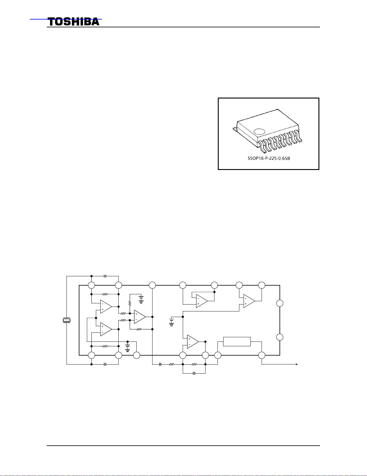
Block Diagram
Weight: 0.07 g (typ.)
TB6066FNG
C1
15 16
50 MΩ
0.63 V
50 MΩ
1
C2
2
Guard
1 V
Diff Amp
×5
3
14
1.2 V
C3 R1 R2
13 12
OP2 AMP
OP3 AMP
4 5
C4
Comparator
6
11 10
OP1 AMP
7
V
9
CC
GND
8
“L” output when shock
detected.
1
2003-05-14
Pin Function
Pin No. Pin Name Function
1 SIA Connection terminal of shock sensor
2 SOA Amp (A) output terminal
3 VR Guard terminal. Reference voltage to protect (1, 16 pin)
4 A3I OP-AMP (3) input terminal
5 A3O OP-AMP (3) output terminal
6 CMI Comparator Input terminal
7 CMO Comparator Output terminal (output = “L” when shock is detected.)
8 GND Ground terminal
9 VCC Power supply voltage
10 A1O OP-AMP (1) output terminal
11 A1I OP-AMP (1) input terminal
12 A2O OP-AMP (2) output terminal
13 A2I OP-AMP (2) input terminal
14 DO Differential-Amp output terminal
15 SOB Amp (B) output terminal
16 SIB Connection terminal of shock sensor
Pin Connection
(top view)
TB6066FNG
SIA
SOA
VR
A3I
A3O
CMI
CMO
GND
1
2
3
4
5
6
7
8
16
15
14
13
12
11
10
9
SIB
SOB
DO
A2I
A2O
A1I
A1O
V
CC
2
2003-05-14

TB6066FNG
Maximum Ratings
Characteristics Symbol Rating Unit
Power supply voltage VCC 6 V
Input voltage VIN −0.3 to VCC + 0.3 V
Power dissipation PD 300 mW
Storage temperature T
(Ta = 25°C)
−55 to 150 °C
stg
Recommend Operating Condition
Characteristics Symbol Rating Unit
Power supply voltage VCC 2.7 to 5.5 V
Operating temperature T
Note: The IC may be destroyed due to short circuit between adjacent pins, incorrect orientation of device’s mounting,
connecting positive and negative power supply pins wrong way round, air contamination fault, or fault by
improper grounding.
−25 to 85 °C
opr
3
2003-05-14
Electrical Characteristics (1) --- Guaranteed data
(unless otherwise specified, VCC = 3.3 V, Ta = 25°C)
TB6066FNG
Characteristics Symbol
Supply voltage VCC 2.7 3.3 5.5 V
Supply current ICC 1
Test
Circuit
Test Condition Min Typ. Max Unit
VCC = 3.3 V 3.5 5
V
= 5.0 V 3.6 5
CC
mA
(DIFF-AMP)
Characteristics Symbol
Gain GvBuf 2 13.6 14 14.4 dB
Output DC voltage VoBuf 3
Output source current IBso 4 Voh = VCC − 1 V 0.6 1.9 mA
Output sink current IBsi 5 Vol = 0.3 V 70 150 µA
Test
Circuit
Test Condition Min Typ. Max Unit
Connect C = 1000 pF between
1 pin and 2 pin,
15 pin and 16 pin,
0.7 1 1.3 V
(OP-AMP1)
Characteristics Symbol
Input voltage 1 Vin1 6 1.135 1.2 1.265 V
Input current Iin 7 40 100 nA
Output voltage range (Low side) Vol 0.3 V
Output voltage range (High side) Voh VCC − 1V
Output source current IAso 8 Voh = VCC − 1 V 200 800 µA
Output sink current IAsi 9 Vol = 0.3 V 100 200 µA
Test
Circuit
Test Condition Min Typ. Max Unit
(OP-AMP2)
Characteristics Symbol
Input voltage range (Low side) Vil 0 V
Input voltage range (High side) Vih VCC − 1V
Input current Iin 10 Input voltage 1.0 V −100 100 nA
Output voltage range (Low side) Vol 0.3 V
Output voltage range (High side) Voh VCC − 1V
Output source current IAso 11 Voh = VCC − 1 V 200 800 µA
Output sink current IAsi 12 Vol = 0.3 V 100 200 µA
Test
Circuit
Test Condition Min Typ. Max Unit
4
2003-05-14

TB6066FNG
(OP-AMP3)
Characteristics Symbol
Input voltage 1 Vin1 13 1.135 1.2 1.265 V
Input current Iin 14 40 100 nA
Output voltage range (Low side) Vol 0.3 V
Output voltage range (High side) Voh VCC − 1V
Output source current IAso 15 Voh = VCC − 1 V 200 800 µA
Output sink current IAsi 16 Vol = 0.3 V 100 200 µA
(Window-Comparator)
Characteristics Symbol
Output pull-up resistance RWu 17 21 27 33 kΩ
Output sink current IWsi 18 Vol = 0.3 V 1.0 3.0 mA
(Guard Terminal)
Characteristics Symbol
Reference Voltage V
ref
Test
Circuit
Test
Circuit
Test
Circuit
0.50 0.63 0.80 V
Test Condition Min Typ. Max Unit
Test Condition Min Typ. Max Unit
Test Condition Min Typ. Max Unit
Note: This terminal should be used to make guard ring for (1, 16 pin). Please don’t use for any other usage.
5
2003-05-14

TB6066FNG
Electrical Characteristics (2) --- Reference data for application (Note)
(DIFF-AMP)
Characteristics Symbol
Input impedance Zin 30 100 MΩ
(OP-AMP1/2/3)
Characteristics Symbol
Cut-off frequency fT 500 kHz
Openloop gain Gvo 80 90 dB
Offset voltage (OP-AMP1/3) Voff −5 0 5 mV
Offset voltage (OP-AMP2) Voff −15 0 15 mV
(Window-Comparator)
Characteristics Symbol
Trip voltage 1 Vtrp1
Test
Circuit
Test
Circuit
Test
Circuit
Test Condition Min Typ. Max Unit
Test Condition Min Typ. Max Unit
Test Condition Min Typ. Max Unit
Vin1
Vin1
±0.37
±0.4
Vin1
±0.43
V
Note: Toshiba can not test these tables of characteristics for all samples. Therefore Toshiba does not guarantee the
data. Please use the data as reference data for customer’s application.
6
2003-05-14

Application Note
=
16
Shock
sensor
Qs (pC/G)
1
Figure 1 The Configuration of G-Force Sensor Amplifier
Figure 1 shows the configuration of G-Force sensor amplifier.
The shock sensor is connected between the pins 1 and 16.
< How to output 0 or 1 from the pin 7 to detect whether there is a shock or not. >
– Using a sensor with the sensitivity Qs (pC/G) to detect the shock g (G). –
a. Setting gain: C1 = C2 (pF), R1 (kΩ), R2 (kΩ)
gQs
×
C1
C1
50 MΩ
50 MΩ
C2
52
15
2
R2
R1
TB6066FNG
1.6 V
C4
R2
×5
14 4
(V)0.4
=×××
R1 C3
5 6
1.2 V
0.8 V
7
Example: Detecting 5 (G)-shock using a sensor
with Qs = 0.34 (pC/G), R1 = 10 (kΩ), R2 = 100 (kΩ).
R2
gQs
C2C1 ×
×
==
0.04
R1
C2C1 =×
==
0.04
100
50.34
×
10
(pF)425
b. Setting the frequency (Hz) of HPF: Setting C3 (µF), R1 (kΩ)
(Hz)fc ×
=
1
3
10
C3R12
××π×
Example: Setting the frequency to 20 Hz with
R1 = 10 (kΩ).
C3 µ=×
=
1
××π×
3
10
20102
F)(0.8
c. Setting the frequency (kHz) of LPF: Setting C4 (pF), R2 (kΩ)
(kHz)fc ×
=
1
6
10
C4R22
××π×
Example: Setting the frequency to 5 kHz with
R2 = 100 (kΩ).
C4 =×
=
1
6
10
51002
××π×
(pF)318
< How to output the voltage according to the shock through the pin 5. >
– Using a sensor with the sensitivity Qs (pC/G), and assuming the shock sensitivity of the system is
Vsystem (mV/G). –
a. Setting gain: C1 = C2 (pF), R1 (kΩ), R2 (kΩ)
Qs
C1
R2
R1
Vsystem
52
3
×=×××
10
(mV/G)
Example: Designing the system with 200 (mV/G)
by using a sensor that Qs = 0.34 (pC/G),
R1
10 (kΩ), R2 = 100 (kΩ).
C2C1
Qs
Vsystem
R2
R1
100
4
××==
(pF)
10
7
0.34
C2C1 =××==
200
10
10
4
(pF)170
2003-05-14

Equivalent Circuit
VCC
TB6066FNG
VCC
VCC
100 Ω
14
DO
100 Ω
12
A2O
100 Ω
10
A1O
VCC
100 Ω
5
A3O
0.8 V
6
CMI
1.6 V
27 kΩ
7
CMO
8
2003-05-14

Test Circuit
(1) Supply current: I
2 MΩ 2 MΩ
5 kΩ
1
SIA
2
SOA
3
VR
4
A3I
5
A3O
6
CMI
7
CMO
8
GND
(2) DIFF-AMP
Gain: GvBuf Gain = (M2-M1)/(0.63-0.47)
Step 1 Step 2
1
SIA
5 kΩ
2
SOA
3
VR
4
A3I
5
A3O
6
CMI
7
CMO
8
GND
2 MΩ
2 MΩ
0.63 V
CC
16
SIB
15
SOB
14
DO
13
A2I
12
A2O
A1I
A1O
VCC
SIB
SOB
DO
A2I
A2O
A1I
A1O
VCC
11
10
9
16
15
14
13
12
11
10
9
5 kΩ
A
2 MΩ
M1
3.3 V
1
SIA
5 kΩ
2
SOA
3
VR
4
A3I
5
A3O
6
CMI
7
CMO
8
GND
2 MΩ
V
2 MΩ
0.63 V
2 MΩ
0.63 V
TB6066FNG
16
SIB
SOB
DO
A2I
A2O
A1I
A1O
VCC
15
14
13
12
11
10
9
2 MΩ
M2
V
2 MΩ
0.47 V
3.3 V
3.3 V
(3) DIFF-AMP
Output DC voltage: VoB uf
1000 pF
5 kΩ
1
SIA
2
SOA
3
VR
4
A3I
5
A3O
6
CMI
7
CMO
8
GND
SIB
SOB
DO
A2I
A2O
A1I
A1O
VCC
16
15
14
13
12
11
10
9
1000 pF
V
3.3 V
9
2003-05-14

TB6066FNG
(4) DIFF-AMP (5) DIFF-AMP
Output source current: IBso Output sink current: IBsi
2 MΩ
2 MΩ
5 kΩ
1
SIA
2
SOA
3
VR
4
A3I
5
A3O
6
CMI
7
CMO
8
GND
SIB
SOB
DO
A2I
A2O
A1I
A1O
VCC
16
15
14
13
12
11
10
9
2 MΩ
2 MΩ
A
2.3 V
5 kΩ
1
SIA
2
SOA
3
VR
4
A3I
5
A3O
6
CMI
7
CMO
8
GND
SIB
SOB
DO
A2I
A2O
A1I
A1O
VCC
16
15
14
13
12
11
10
9
2 MΩ
A
2 MΩ
0.3 V
3.3 V
3.3 V
(6) OP-AMP1 (7) OP-AMP1
Input voltage 1: Vin1 Input current: Iin
5 kΩ
1
SIA
2
SOA
3
VR
4
A3I
5
A3O
6
CMI
7
CMO
8
GND
SIB
SOB
DO
A2I
A2O
A1I
A1O
VCC
16
15
14
13
12
11
10
9
5 kΩ
5 kΩ
V
3.3 V
1
SIA
2
SOA
3
VR
4
A3I
5
A3O
6
CMI
7
CMO
8
GND
Spec (Iin) = IM/2
SIB
SOB
DO
A2I
A2O
A1I
A1O
VCC
16
15
14
13
12
11
10
9
I
M
A
0.6 V
3.3 V
(8) OP-AMP1 (9) OP-AMP1
Output source current: IAso Output sink current: IAsi
5 kΩ
1
SIA
2
SOA
3
VR
4
A3I
5
A3O
6
CMI
7
CMO
8
GND
SIB
SOB
DO
A2I
A2O
A1I
A1O
VCC
16
15
14
13
12
11
10
9
5 kΩ
A
1
SIA
2
SOA
3
VR
4
A3I
5
A3O
6
CMI
7
CMO
8
GND
SIB
SOB
DO
A2I
A2O
A1I
A1O
VCC
16
15
14
13
12
11
10
9
A
1.0 V
2.3 V
3.3 V
3.3 V
1.4 V
0.3 V
10
2003-05-14

TB6066FNG
(10) OP-AMP2
Input current: Iin
1
SIA
2
SOA
3
VR
5 kΩ
4
A3I
5
A3O
6
CMI
7
CMO
8
GND
Spec (Iin) = IM
(11) OP-AMP2 (12) OP-AMP2
Output source current: IAso Output sink current: IAsi
1
SIA
2
SOA
3
VR
5 kΩ
4
A3I
5
A3O
6
CMI
7
CMO
8
GND
SIB
SOB
DO
A2I
A2O
A1I
A1O
VCC
SIB
SOB
DO
A2I
A2O
A1I
A1O
VCC
16
15
14
13
12
11
10
9
16
15
14
13
12
11
10
9
I
3.3 V
M
A
1.0 V
1
SIA
2
SOA
3
VR
5 kΩ
A
3.3 V
2.3 V
4
A3I
5
A3O
6
CMI
7
CMO
8
GND
SIB
SOB
DO
A2I
A2O
A1I
A1O
VCC
16
15
14
13
12
11
10
9
A
0 V
0.3 V
3.3 V
3.3 V
(13) OP-AMP3 (14) OP-AMP3
Input voltage 1: Vin1 Input current: Iin
1
SIA
2
SOA
3
VR
4
A3I
5 kΩ
V
5
A3O
6
CMI
7
CMO
8
GND
SIB
SOB
DO
A2I
A2O
A1I
A1O
VCC
16
15
14
13
12
11
10
9
I
M
A
0.6 V
3.3 V
1
SIA
2
SOA
3
VR
4
A3I
5
A3O
6
CMI
7
CMO
8
GND
Spec (Iin) = IM/2
SIB
SOB
DO
A2I
A2O
A1I
A1O
VCC
16
15
14
13
12
11
10
9
3.3 V
11
2003-05-14

TB6066FNG
(15) OP-AMP3 (16) OP-AMP3
Output source current: IAso Output sink current: IAsi
1
SIA
2
SOA
3
VR
4
A3I
5
A3O
A
2.3 V
1.0 V
6
CMI
7
CMO
8
GND
SIB
SOB
DO
A2I
A2O
A1I
A1O
VCC
16
15
14
13
12
11
10
A
9
0.3 V
1.4 V
1
SIA
2
SOA
3
VR
4
A3I
5
A3O
6
CMI
7
CMO
8
GND
SIB
SOB
DO
A2I
A2O
A1I
A1O
VCC
16
15
14
13
12
11
10
9
3.3 V
3.3 V
(17) Window comparator (18) Window comparator
Output pull-up resistance: RWu Output sink current: Iwsi
M3
A
1.2 V
1
SIA
2
SOA
3
VR
4
A3I
5
A3O
6
CMI
7
CMO
8
GND
RWu = 3.3/M3
SIB
SOB
DO
A2I
A2O
A1I
A1O
VCC
16
15
14
13
12
11
10
9
3.3 V
A
0.7 V
0.3 V
1
SIA
2
SOA
3
VR
4
A3I
5
A3O
6
CMI
7
CMO
8
GND
SIB
SOB
DO
A2I
A2O
A1I
A1O
VCC
16
15
14
13
12
11
10
9
3.3 V
12
2003-05-14

Package Dimensions
TB6066FNG
Weight: 0.07 g (typ.)
13
2003-05-14

TB6066FNG
RESTRICTIONS ON PRODUCT USE
• TOSHIBA is continually working to improve the quality and reliability of its products. Nevertheless, semiconductor
devices in general can malfunction or fail due to their inherent electrical sensitivity and vulnerability to physical
stress. It is the responsibility of the buyer, when utilizing TOSHIBA products, to comply with the standards of
safety in making a safe design for the entire system, and to avoid situations in which a malfunction or failure of
such TOSHIBA products could cause loss of human life, bodily injury or damage to property.
In developing your designs, please ensure that TOSHIBA products are used within specified operating ranges as
set forth in the most recent TOSHIBA products specifications. Also, please keep in mind the precautions and
conditions set forth in the “Handling Guide for Semiconductor Devices,” or “TOSHIBA Semiconductor Reliability
Handbook” etc..
• The TOSHIBA products listed in this document are intended for usage in general electronics applications
(computer, personal equipment, office equipment, measuring equipment, industrial robotics, domestic appliances,
etc.). These TOSHIBA products are neither intended nor warranted for usage in equipment that requires
extraordinarily high quality and/or reliability or a malfunction or failure of which may cause loss of human life or
bodily injury (“Unintended Usage”). Unintended Usage include atomic energy control instruments, airplane or
spaceship instruments, transportation instruments, traffic signal instruments, combustion control instruments,
medical instruments, all types of safety devices, etc.. Unintended Usage of TOSHIBA products listed in this
document shall be made at the customer’s own risk.
• The information contained herein is presented only as a guide for the applications of our products. No
responsibility is assumed by TOSHIBA CORPORATION for any infringements of intellectual property or other
rights of the third parties which may result from its use. No license is granted by implication or otherwise under
any intellectual property or other rights of TOSHIBA CORPORATION or others.
• The information contained herein is subject to change without notice.
000707EAA
14
2003-05-14
 Loading...