Toshiba TA DA9000ES Service Manual
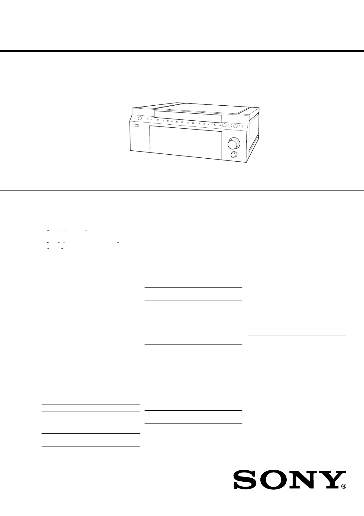
TA-DA9000ES
SERVICE MANUAL
Ver 1.2 2004.09
This amplifier incorporates Dolby* Digital and Pro
Logic Surround and the DTS** Digital Surround
System.
Manufactured under license from Dolby
*
Laboratories.
Dolby
, Pro Logic and the double-D symbol are
trademarks of Dolby Laboratories.
** DTS
,DTS-ES Extended Surround , and
Neo:6 are trademarks of Digital Th eater Systems,
Inc.
AEP Model
E Model
Amplifier section
POWER OUTPUT
Rated Power Output at Stereo Mode
(8 ohms, 20 Hz − 20 kHz, THD 0.15%)
200 W + 200 W
(4 ohms, 20 Hz − 20 kHz, THD 0.15%)
220 W + 220 W
Reference Power Output
(8 ohms, 1 kHz, THD 0.09%)
FRONT
CENTER
SURR
SURR BACK
(4 ohms, 1 kHz, THD 0.09%)
FRONT
CENTER
SURR
SURR BACK
1) Depending on the sound field settings and the
source, there may be no sound output.
2) Measured under the following conditio ns :
Area code Power requirements
CEL 230 V AC, 50/60 Hz
TW 110 V AC, 60 Hz
KR 230 V AC, 60 Hz
Frequency response
PHONO RIAA equalization curve
±0.5 dB
1)
2)
: 200 W + 200 W
2)
: 200 W
2)
: 200 W + 200 W
2)
: 200 W + 200 W
2)
: 220 W + 220 W
2)
: 220 W
2)
: 220 W + 220 W
2)
: 220 W + 220 W
SPECIFICATIONS
Power Amp Block 10 Hz − 50 kHz
± 3 dB (8 ohms)
Inputs (Analog)
PHONO Sensitivity: 3.5 mV
Impedance: 50 kilohms
S/N3): 90 dB (A, 40 mV4))
CD/SACD, TAPE,
MD/DAT, DVD, LD,
TV/SAT, VIDEO 1, 2,
3, 4, 5
3) Input shorted and sealed at VOL MAX.
4) Weighted network + 20 kHz LPF, input level.
Inputs (Digital)
CD/SACD, DVD, LD,
VIDEO 1, TV/SAT
(Coaxial)
CD/SACD, DVD, LD,
TV/SAT, MD/DAT,
VIDEO1, 3 (Optical)
Outputs
Sensitivity: 170 mV
Impedance: 50 kilohms
3)
: 100 dB (A, 2V4))
S/N
Impedance: 75 ohms
S/N: 100 dB
(A Network, 20 kHz LPF)
S/N: 100 dB
(A Network, 20 kHz LPF)
TAPE, MD/DAT
(REC OUT), VIDEO
1, 2, 3 (AUDIO OUT)
FRONT L/R,
CENTER,
SURROUND L/R,
SURROUND BACK
L/R, SUB WOOFER
EQUALIZER
Gain levels ±10 dB, 1 dB step
Video section
Inputs/Outputs
Video: 1 Vp-p, 75 ohms
S-video: Y: 1 Vp-p, 75 ohms
COMPONENT VIDEO:Y: 1 Vp-p, 75 ohms
Voltage: 170 mV
Impedance: 2.2 kilohms
Voltage: 2 V
Impedance: 220 ohms
C: 0.286 Vp-p, 75 ohms
/B-Y: 0.7 Vp-p, 75
P
B/CB
ohms
P
/R-Y: 0.7 Vp-p, 75
R/CR
ohms
– Continued on next page –
MULTI-CHANNEL INTEGRATED AMPLIFIER
9-961-291-03 Sony Corporation
2004I05-1 Audio Group
© 2004.09 Published by Sony Engineering Corporation

TA-DA9000ES
i.LINK section
Pin 4 pins
Transmission speed S200 (Maximum data
transmission speed 200
Mbps)
Transmission protocol A/M transmission protocol
Format (input) Super Audio CD* (DSD
PLAIN)
2 channel linear PCM (IEC-
60958-3)
Sampling frequency: 44.1
kHz
* Conforms to the copy protection technology of
DTLA (Revision 1.2).
General
Power requirements
Area code Power requirements
AEP 230 V AC, 50/60 Hz
Taiwan 110 V AC, 60 Hz
Area code Power requirements
Korean 220 V AC, 60 Hz
Power consumption 600 W
Power consumption (during standby mode)
1 W
AC outlets
Area code AC outlets
AEP 1 switched, 100 W MAX
except AEP − (no AC outlet)
Dimensions 430 × 238 × 480 mm
including projecting parts and
controls
Mass (Approx.) 28.5 kg
Supplied accessories
AC power coad (1)
Easy Setup Guide (1)
Remote commander RM-LJ312 (1)
Operating Instructions for RM-LJ312 (1)
R6 (size-AA) batteries (3)
Design and specifications are subject to change
without notice.
SAFETY-RELATED COMPONENT WARNING!!
COMPONENTS IDENTIFIED BY MARK 0 OR DOTTED
LINE WITH MARK 0 ON THE SCHEMATIC DIAGRAMS
AND IN THE PARTS LIST ARE CRITICAL TO SAFE
OPERATION. REPLACE THESE COMPONENTS WITH
SONY PARTS WHOSE PART NUMBERS APPEAR AS
SHOWN IN THIS MANU AL OR IN SUPPLEMENTS PUBLISHED BY SONY.
2
Notes on chip component replacement
• Never reuse a disconnected chip component.
• Notice that the minus side of a tantalum capacitor may be damaged by heat.
: LEAD FREE MARK
Unleaded solder has the following characteristics.
• Unleaded solder melts at a temperature about 40 ˚C higher than
ordinary solder.
Ordinary soldering irons can be used but the iron tip has to be
applied to the solder joint for a slightly longer time.
Soldering irons using a temperature regulator should be set to
about 350 ˚C.
Caution: The printed pattern (copper foil) may peel away if the
heated tip is applied for too long, so be careful!
• Strong viscosity
Unleaded solder is more viscou-s (sticky, less prone to flow)
than ordinary solder so use caution not to let solder bridges occur such as on IC pins, etc.
• Usable with ordinary solder
It is best to use only unleaded solder but unleaded solder may
also be added to ordinary solder.

TABLE OF CONTENTS
TA-DA9000ES
1. SERVICING NOTES............................................... 5
2. GENERAL
Location of Controls ....................................................... 10
3. DISASSEMBLY
3-1. Disassembly Flow ........................................................... 12
3-2. Case (Top)/(Side-L)/(Side-R) ......................................... 13
3-3. Bracket (J)/(P-B) ............................................................. 13
3-4. AMP Board Block........................................................... 14
3-5. COMPONENT Board Section........................................ 14
3-6. S-VIDEO/VIDEO Board Block ..................................... 15
3-7. SUB Board, PREOUT Board, MAIN Board.................. 15
3-8. I. LINK Board, DIGITAL Board .................................... 16
3-9. MOTHER Board Section................................................ 16
3-10. MOTHER Board ............................................................. 17
4. TEST MODE.............................................................. 18
5. ELECTRICAL ADJUSTMENTS ......................... 21
6. DIAGRAMS
6-1. Block Diagram – AUDIO INPUT Section – ................. 23
6-2. Block Diagram – A/D CONVERTER Section – ........... 24
6-3. Block Diagram – DIGITAL INPUT Section –.............. 25
6-4. Block Diagram – I. LINK Section –.............................. 26
6-5. Block Diagram – DSP Section – ................................... 27
6-6. Block Diagram – DIGIT AL AUDIO Section – ............. 28
6-7. Block Diagram – AUDIO OUTPUT Section – ............. 29
6-8. Block Diagram – POWER AMP Section – ................... 30
6-9. Block Diagram – VIDEO INPUT/OUT Section –........ 31
6-10. Block Diagram – COMPONENT VIDEO Section – .... 32
6-11. Block Diagram – DISPLAY/CONTROL Section –...... 33
6-12. Block Diagram – POWER SUPPLY Section – ............. 34
6-13. Note for Printed Wiring Boards
and Schematic Diagrams ................................................ 35
6-14. Printed W iring Board
– DIGITAL Board (Component Side) – ......................... 36
6-15. Printed W iring Board
– DIGITAL Board (Conductor Side) –........................... 37
6-16. Schematic Diagram – DIGITAL Board (1/11) –........... 38
6-17. Schematic Diagram – DIGITAL Board (2/11) –........... 39
6-18. Schematic Diagram – DIGITAL Board (3/11) –........... 40
6-19. Schematic Diagram – DIGITAL Board (4/11) –........... 41
6-20. Schematic Diagram – DIGITAL Board (5/11) –........... 42
6-21. Schematic Diagram – DIGITAL Board (6/11) –........... 43
6-22. Schematic Diagram – DIGITAL Board (7/11) –........... 44
6-23. Schematic Diagram – DIGITAL Board (8/11) –........... 45
6-24. Schematic Diagram – DIGITAL Board (9/11) –........... 46
6-25. Schematic Diagram – DIGITAL Board (10/11) –......... 47
6-26. Schematic Diagram – DIGITAL Board (11/11) –......... 48
6-27. Schematic Diagram – MAIN Board (1/3) – .................. 49
6-28. Schematic Diagram – MAIN Board (2/3) – .................. 50
6-29. Schematic Diagram – MAIN Board (3/3) – .................. 51
6-30. Printed W iring Board
– MAIN Board (Component Side) – .............................. 52
6-31. Printed W iring Board
– MAIN Board (Conductor Side) – ................................ 53
6-32. Printed W iring Board
– SUB Board (Component Side) – ................................. 54
6-33. Printed W iring Board
– SUB Board (Conductor Side) – ................................... 55
6-34. Schematic Diagram – SUB Board (1/2) –..................... 56
6-35. Schematic Diagram – SUB Board (2/2) –..................... 57
6-36. Printed W iring Board
– I. LINK Board (Component Side) – ............................ 58
6-37. Printed Wir ing Board
– I. LINK Board (Conductor Side) –.............................. 59
6-38. Schematic Diagram – I. LINK Board (1/4) –................ 60
6-39. Schematic Diagram – I. LINK Board (2/4) –................ 61
6-40. Schematic Diagram – I. LINK Board (3/4) –................ 62
6-41. Schematic Diagram – I. LINK Board (4/4) –................ 63
6-42. Printed Wiring Board – PREOUT Board – ................... 64
6-43. Schematic Diagram – PREOUT Board – ...................... 65
6-44. Printed Wiring Board – VIDEO Board –....................... 66
6-45. Schematic Diagram – VIDEO Board – ......................... 67
6-46. Printed Wiring Board – S-VIDEO Board –................... 68
6-47. Schematic Diagram – S-VIDEO Board – ...................... 69
6-48. Printed Wir ing Board
– COMPONENT Section (Component Side) –.............. 70
6-49. Printed W iring Boards
– COMPONENT Section (Conductor Side) – ............... 71
6-50. Schematic Diagram
– COMPONENT Section (1/4) –.................................... 72
6-51. Schematic Diagram
– COMPONENT Section (2/4) –.................................... 73
6-52. Schematic Diagram
– COMPONENT Section (3/4) –.................................... 74
6-53. Schematic Diagram
– COMPONENT Section (4/4) –.................................... 75
6-54. Printed Wir ing Board
– MOTHER Board (Component Side) – ........................ 76
6-55. Printed Wir ing Board
– MOTHER Board (Conductor Side) –.......................... 77
6-56. Schematic Diagram – MOTHER Board (1/3) –............ 78
6-57. Schematic Diagram – MOTHER Board (2/3) –............ 79
6-58. Schematic Diagram – MOTHER Board (3/3) –............ 80
6-59. Schematic Diagram – AMP Board (1/5) – .................... 81
6-60. Schematic Diagram – AMP Board (2/5) – .................... 82
6-61. Schematic Diagram – AMP Board (3/5) – .................... 83
6-62. Schematic Diagram – AMP Board (4/5) – .................... 84
6-63. Schematic Diagram – AMP Board (5/5) – .................... 85
6-64. Printed Wir ing Board
– AMP Board (Component Side) – ................................ 86
6-65. Printed Wir ing Board
– AMP Board (Conductor Side) – .................................. 87
6-66. Printed Wiring Board – FCOIL Board – ....................... 88
6-67. Schematic Diagram – FCOIL Board – .......................... 89
6-68. Printed Wiring Board – RCOIL Board –....................... 90
6-69. Schematic Diagram – RCOIL Board –.......................... 91
6-70. Printed Wiring Boards – SP Section –........................... 92
6-71. Schematic Diagram – SP Section – ............................... 93
6-72. Printed Wiring Board – DISPLAY Section – ................ 94
6-73. Schematic Diagram – DISPLAY Section –................... 95
6-74. Printed Wiring Boards – PANEL Section – .................. 96
6-75. Schematic Diagram – PANEL Section –....................... 97
6-76. Printed Wir ing Board
– DC Board (Component Side) – ................................... 98
6-77. Printed Wir ing Board
– DC Board (Conductor Side) – ..................................... 99
6-78. Schematic Diagram – DC Board – ............................... 100
6-79. Printed Wiring Board – AC Board –............................. 101
6-80. Schematic Diagram – AC Board –................................ 102
6-81. IC Pin Function Description .......................................... 119
3

TA-DA9000ES
7. EXPLODED VIEWS
7-1. Case Section ................................................................... 141
7-2. Disp Board Section ........................................................ 142
7-3. Volume Section .............................................................. 143
7-4. Panel (Door) Section...................................................... 144
7-5. Front Panel Section ........................................................ 145
7-6. Base Panel Section ......................................................... 146
7-7. AMP Board Section ....................................................... 147
7-8. Component Board Section ............................................. 148
7-9. Main Board Section ....................................................... 149
7-10. Digital/I. Link Board Section ........................................ 150
7-11. Back Panel Section......................................................... 151
7-12. Transformer Section....................................................... 152
7-13. MOTHER Board Section ...............................................153
8. ELECTRICAL PARTS LIST .............................. 154
4
TA-DA9000ES
SECTION 1
SERVICING NOTES
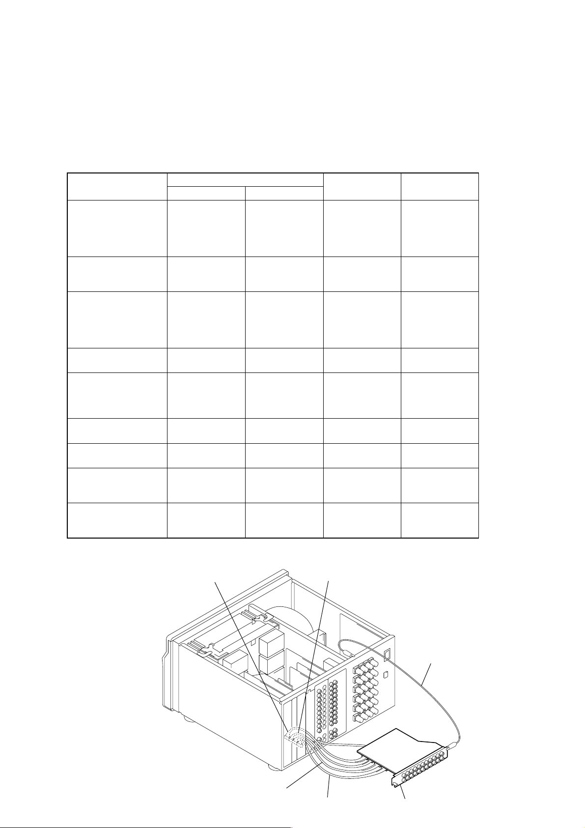
NOTES ON REPLACEMENT OF I. LINK BOARD
New part of microcomputer (IC3002) and EEPROM (IC3001) on the I. LINK board cannot be used. Therefore, if the mounted I. LINK
board (A-4733-835-A) is replaced, exchange new microcomputer and new EEPROM with that used before the replacement.
OPERATION CHECK OF STANDING BOARDS ON THE MOTHER BOARD
The standing boards connected to the MOTHER board via the connectors can be operated using the jig with the standing boards disconnected from the MOTHER board.
In such a case, for the board with the bracket (back panel), remove the board together with the bracket from the MOTHER board, and
connect the bracket to the chassis using a cable attached with alligator clips for GND connection.
Board
DIGITAL board CN2001 CNS801 1.25mm/20 pin J-2501-260-A
I. LINK board CN3501 CNS806 1.25mm/16 pin J-2501-258-A
MAIN board CN101 CNS810 1.25mm/14 pin J-2501-257-A
PREOUT board CN1201 CNS822 1.25mm/16 pin J-2501-258-A
SUB board CN1003 CNS812 1.25mm/14 pin J-2501-257-A
VIDEO board CN302 CNS816 1.25mm/18 pin J-2501-259-A
S-VIDEO board CN402 CNS817 1.25mm/20 pin J-2501-260-A
COMPONENT board CN1303 CNS819 1.25mm/20 pin J-2501-260-A
AMP board CN1501 CN824 2.5mm/20 pin J-2501-262-A
Ref. No. of connector
Each board MOTHER board
CN2002 CNS802 1.25mm/20 pin J-2501-260-A
CN2003 CNS803 1.25mm/16 pin J-2501-258-A
CN2004 CNS804 1.25mm/18 pin J-2501-259-A
CN2005 CNS805 1.25mm/20 pin J-2501-260-A
CN3502 CNS807 1.25mm/18 pin J-2501-259-A
CN3503 CNS808 1.25mm/6 pin J-2501-253-A
CN102 CNS811 1.25mm/14 pin J-2501-257-A
CN103 CNS809 1.25mm/8 pin J-2501-254-A
CN104 CNS825 1.25mm/20 pin J-2501-260-A
CN105 CNS824 1.25mm/10 pin J-2501-255-A
CN1203 CNS823 1.25mm/10 pin J-2501-255-A
CN1002 CNS813 1.25mm/14 pin J-2501-257-A
CN1001 CNS814 1.25mm/8 pin J-2501-254-A
CN1006 CNS826 1.25mm/12 pin J-2501-256-A
CN301 CNS815 1.25mm/8 pin J-2501-254-A
CN401 CNS818 1.25mm/6 pin J-2501-253-A
CN1302 CNS820 1.25mm/16 pin J-2501-258-A
CN1301 CNS821 1.25mm/20 pin J-2501-260-A
CN1507 CN816 2.5mm/6 pin J-2501-261-A
CN1508 CN815 2.5mm/6 pin J-2501-261-A
Pitch/Pin Part No. of jig
Example of Connection
connecting jig connecting jig
connecting jig
connecting jig
aligator clip
board
5
TA-DA9000ES
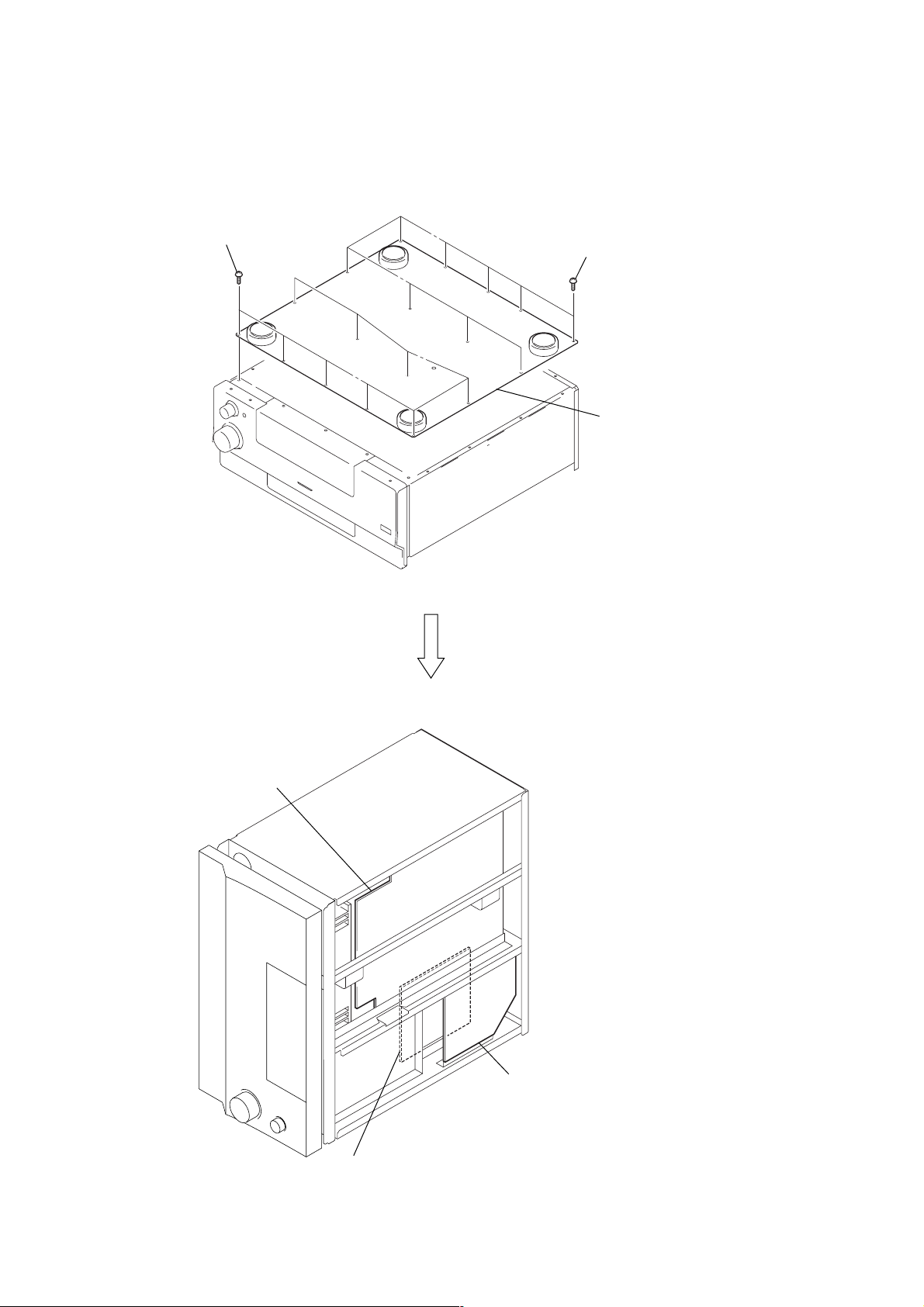
Note: Follow the disassembly procedure in the numerical order given.
– BOTTOM VIEW –
1
nine screws
×
8)
(BV3
2
nine screws
(BV3
3
×
8)
bottom plate
mother board
DC board
FSP board
NOTE:
•
FSP board can be removed in this state.
•
In the same state after removing a FSP board,
the check of DC board can be performed.
6
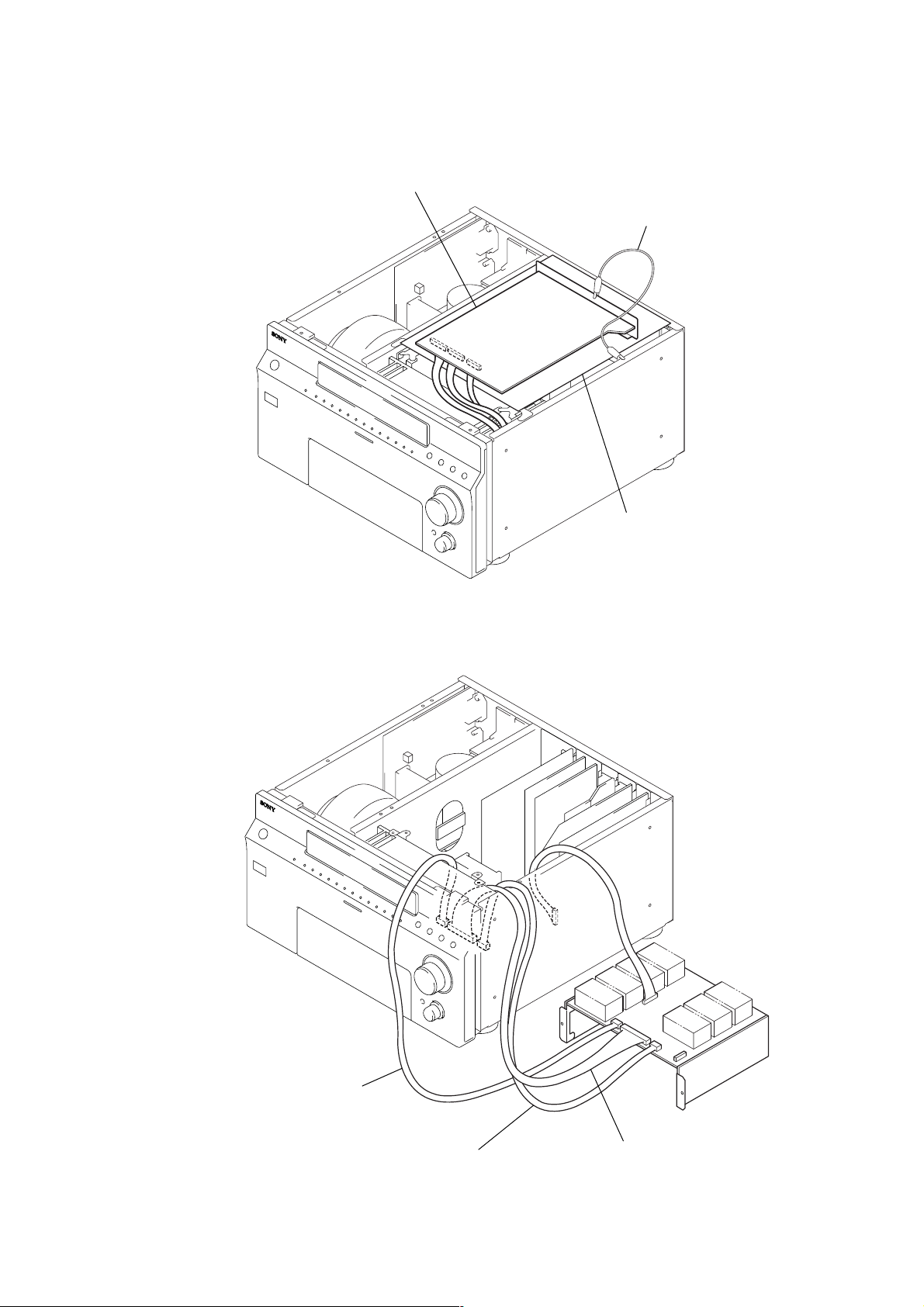
DIGITAL BOARD SERVICE POSITION
Note: Case (top) and Case (side-L)/(side-R) are removed.
digital board
TA-DA9000ES
aligator clip
AMP BOARD SERVICE POSITION
Please place a sheet
for insulation.
Connect jig (J-2501-253-A)
to the AMP board (CN1508)
and mother board (CN815).
Connect jig (J-2501-253-A)
to the AMP board (CN1507)
and mother board (CN816).
Connect jig (J-2501-260-A)
to the AMP board (CN1501)
and mother board (CN824).
7
TA-DA9000ES
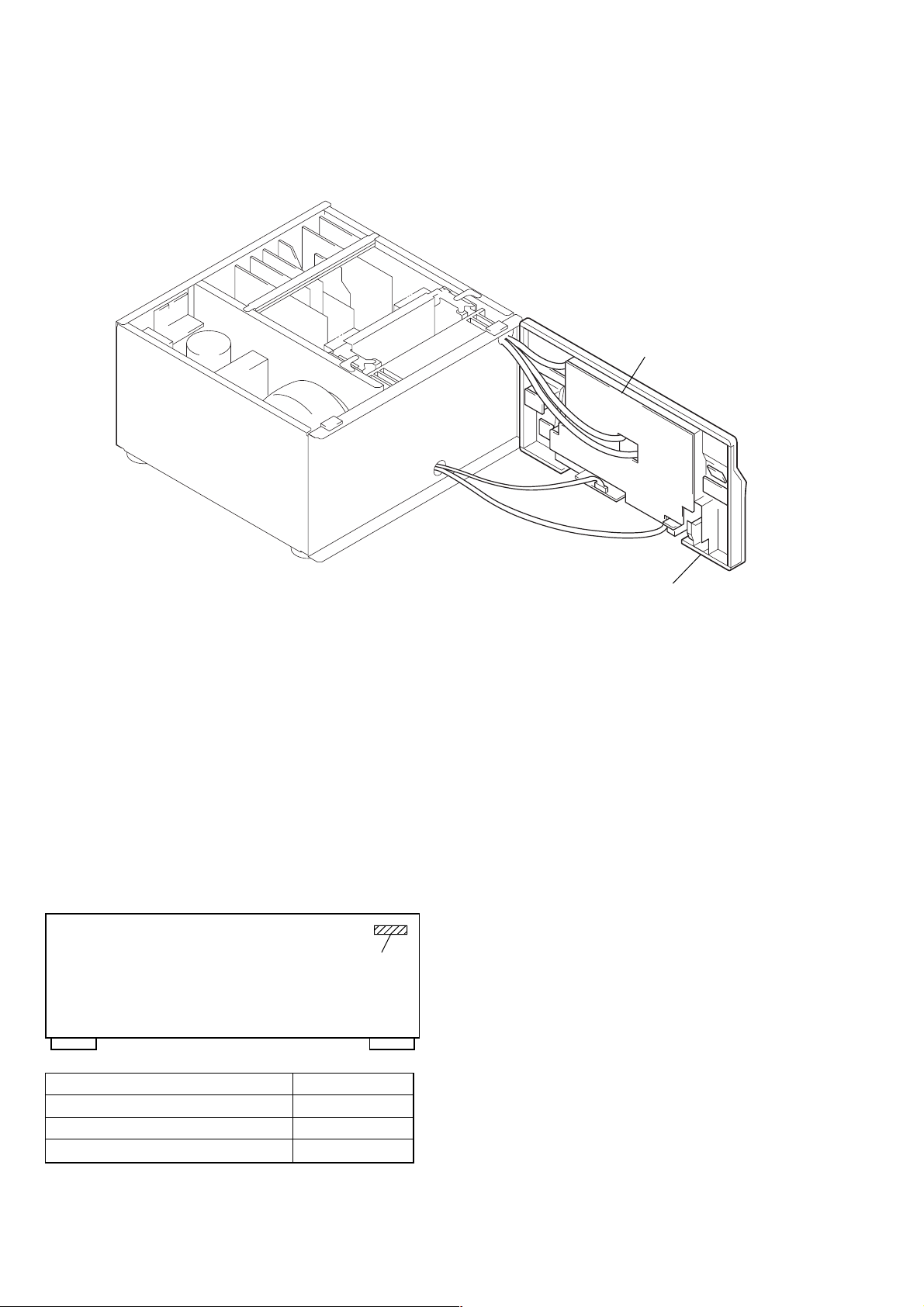
DISP BOARD SERVICE POSITION
Note: Please open a front panel on the right hand side of the set front.
DISP board
• MODEL IDENTIFICATION
– Back Panel –
front panel section
PART No.
Model PART No.
AEP model 4-248-144-1
Korean model 4-248-144-2
Taiwan model 4-248-144-3
8
[]
[]
[]
TA-DA9000ES
Ver 1.2
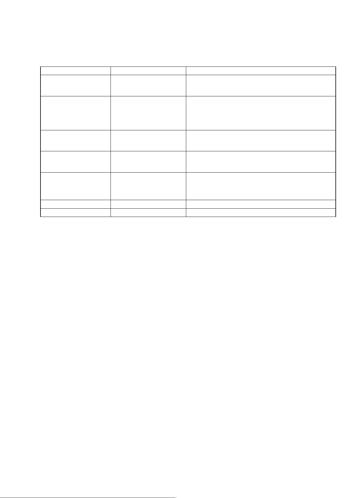
ERROR MESSAGES
If there is a malfunction, the display shows a code of two numbers and a message. You can check the condition of the system by message.
Refer to the following table to solve the problem.
messages check code cause and response
DECODE ERROR 01 Appears when the signal which the receiver can not decode
(example DSD-CD) is input when “DEC. PRI.” in the CUSTOM
IZE menu is set to “PCM”. Set to “AUTO”.
PROTECTOR 11 Irregular current output to the speakers. Turn off the receiver and
check the speaker connection. Then turn on the power again. Be
comes this display, When short current flowed with breakage of
the power MOS, or when detection resistor becomes open in
connection with it.
PROTECTOR 12 The amplifier section is overheated. Turn off the receiver and
check that the ventilation hole is not covered. Leave the receiver
for a while and turn on the power again.
PROTECTOR 13 The power supply section is overheated. Turn off the receiver and
check that the ventilation hole is not covered. leave the receiver
for a while and turn on the power again.
PROTECTOR 21 DC between speaker terminal is detected (abnomalities such as
DSD 0DATA and signal clip can be considered). Turn off the
receiver and check the speaker connection. Then turn on the power
again.
PROHIBITED 71 The receiver can't output the sound due to the copyright protection.
UNKNOWN SIGNAL 72 The receiver isn't compatible with the format of the input signal.
9
TA-DA9000ES
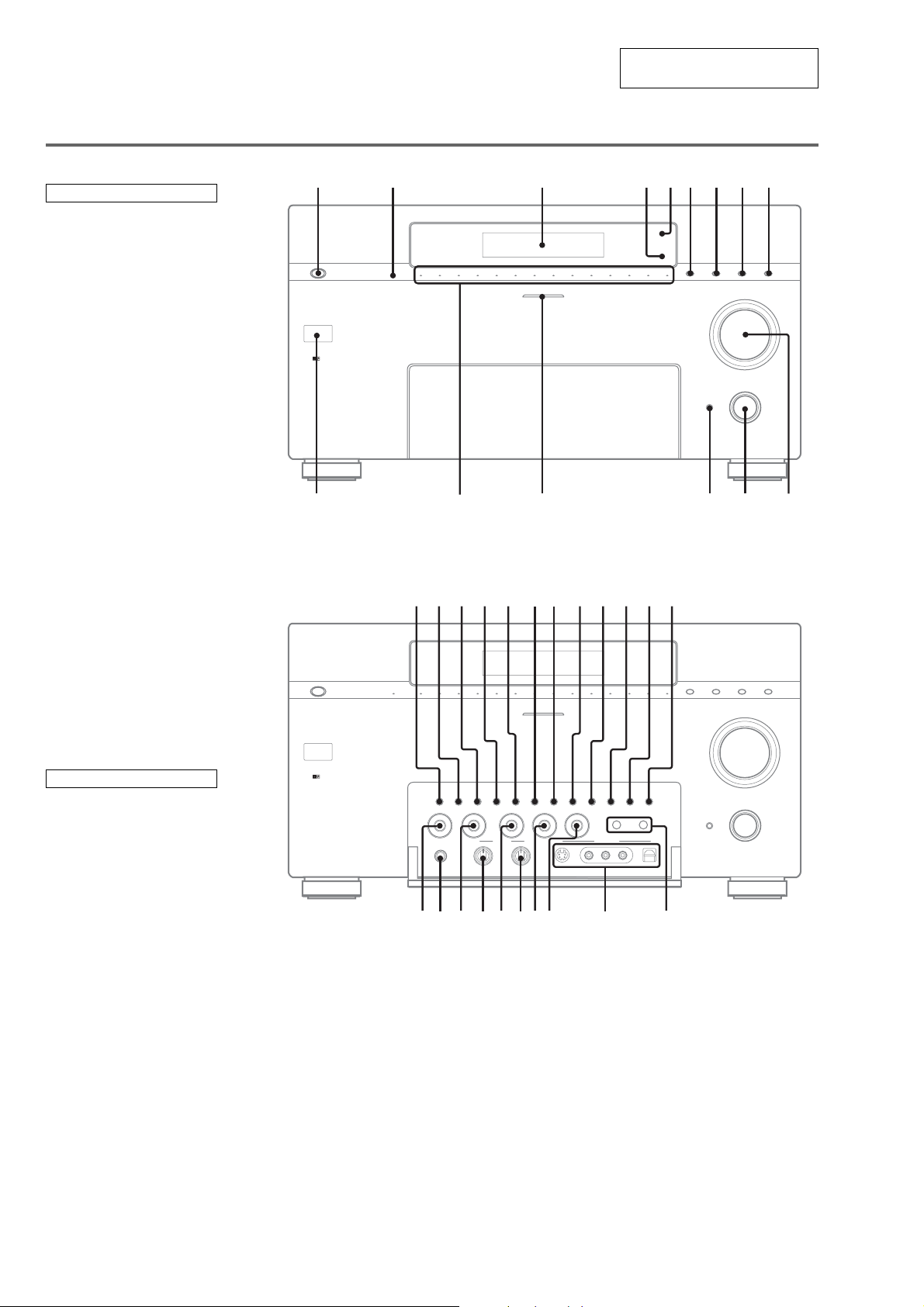
LOCATION OF CONTROLS
SECTION 2
GENERAL
This section is extracted from
instruction manual.
Main unit
ALPHABETICAL ORDER
A.F.D. 7
BASS ej
DECODE PRIORITY wf
Digital Cinema Sound indicator 5
DIMMER qh
DIRECT wg
DIRECT indicator 2
DISPLAY wd
Display 3
ENTER wa
Input indicators qf
INPUT MODE qs
INPUT SELECTOR qa
IR receptor qg
MAIN MENU ed
MASTER VOLUME q;
MENU ea
MOVIE 8
MULTI CH IN 1/2 wh
MULTI CHANNEL DECODING
indicator qd
MUSIC 9
NIGHT MODE qk
ON SCREEN ql
PHONES jack eh
REC OUT SELECTOR +/− wk
SB DEC indicator 4
SLEEP qj
SPEAKERS FRONT switch ef
SPEAKERS SURROUND switch es
SURR BACK DECODING wj
TEST TONE w;
TREBLE eg
USER PRESET ws
VIDEO 5 INPUT jacks wl
1 2 354 7 8 9
qf
qdqg qaqs
6
v
wjqlqkqjqh w; wa ws wd wf
wg wh
0
NUMBERS AND SYMBOLS
2CH 6
?/1 (power) 1
−/+ e;
eh efeg edej es wleae; wk
10

– Remote Commander –
TA-DA9000ES
?/1
AV ?/1TV ?/1
wj
SOUND FIELD
SYSTEM STANDBY
RM SET UP
INPUT SELECTOR
wh
wg
wf
wd
ws
wa
Ii
.> m M
HX x
TOP MENU/GUIDE AV MENU
MASTER
VOL
+
MUTING
w;
ql
qk
qj
DISPLAY
RETURN/EXIT
TV VOL TV CH TV/VIDEO
+—+
—
O
MAIN
MENU
WIDE
—
ON SCREEN
qh
?/1
1
Press to turn the receiver on or off.
AV ?/1
2
Press to turn on or off the components that
the remote is programmed to operate. For
details on programming procedure, see
P rogramming the remote on page 16.
If you press the ?/1 switch (1) at the
same time, it will turn off the main
component and other Sony audio/video
components (SYSTEM STANDBY).
Note
The function of the AV ?/1 switch changes
automatically each time you press INPUT
SELECTOR (4). Depending on the component,
the above operation may not be possible or may
operate differently than described.
AV MENU
ws
Press to display the menus of the VCR,
DVD player, or satellite tuner on the TV
screen. Then use the control button to
perform the menu operations.
Control button
1
2
3
4
5
6
7
8
9
0
qa
qs
DISPLAY
qd
qf
qg
Display window
Easy scroll key
INPUT SELECTOR
MAIN MENU
MASTER VOL +/–
MUTING
ON SCREEN
w;
After pressing MAIN MENU, TOP
MENU/GUIDE, or AV MENU, move the
control button up, down, left or right to
select the settings. When you press TOP
MENU/GUIDE or AV MENU, press the
button to enter the selection.
To perform menu operations on the VCR,
DVD player, or SAT tuner, do the
procedure below. If you do not do this, the
cursor buttons merely operate the receiver.
1
Press INPUT SELECTOR and move the
easy scroll key to select the input, then
press the key to enter the selection.
2
Press MAIN MENU, TOP MENU/
GUIDE, or AV MENU.
The CURSOR TYPE list appears. If the
list has disappeared before you go on to
step 3, press any of the cursor buttons to
restore the list.
3
Move the easy scroll key to select the
component that you selected in step 1,
then press the key to enter the selection.
ql
Press to select information displayed on the
TV screen.
3
The current status of the selected
component or a list of selectable items
appears here.
Note
Characters other than letters of the alphabet or
numbers may be displayed incorrectly on the
remote, even if they appear correctly in the
display window on the main unit.
wg
While displaying a list, move up or down to
select an item from the list, and then press
to enter the selection.
4
Press to display the input (component) list.
qd
Press repeatedly to select a menu
(SURROUND, etc.) for the receiver.
qa
Press to adjust the volume level of all
speakers at the same time.
q;
Press to mute the sound.
qf
Press to display the menus of the receiver
on the TV screen.
RETURN O/EXIT
qk
Press to return to the previous menu or exit
the menu while the menu or guide of the
VCR, DVD player, or satellite tuner is
displayed on the TV screen.
RM SET UP
5
Press to display the set up list.
SOUND FIELD
wh
Press to display the sound field list.
TOP MENU/GUIDE
wa
Press to display the menu or guide of the
DVD player or satellite tuner on the TV
screen. Then use the control button to
perform the menu operations.
TV ?/1
wj
Press to turn TV on or off.
TV/VIDEO
qs
Press to change the input mode of the TV.
TV CH +/–
qh
Press to switch the channel of TV.
TV VOL +/–
qj
Press to adjust the volume of TV.
WIDE
qg
Press to switch the TV to the wide mode.
I/i
6
Press to change the information displayed
on the display. Press the I button
repeatedly to display the RECEIVER
menu, press the i button repeatedly to
display the SUB menu or NUM menu.
In the NUM menu, move the easy scroll key
to select the numeric value, then press the
key to enter the selection.
H
wd
Press to start play of the playback medium.
X
9
Press to pause play or recording, or press to
start recording when the component is in
recording standby.
x
8
Press to stop play.
./>
wf
Press to skip tracks.
m/M
7
Press to fast-forward or rewind, or search
tracks in the forward or backward direction.
11
TA-DA9000ES
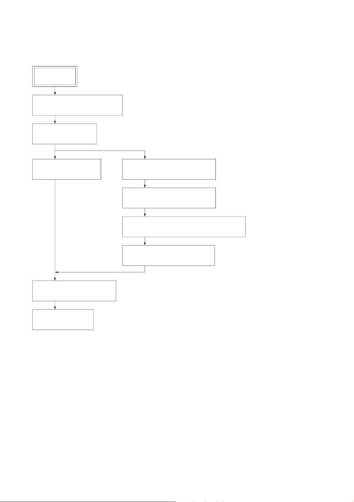
• This set can be disassembled in the order shown below.
3-1. DISASSEMBLY FLOW
SET
3-2. CASE (TOP)/(SIDE-L)/(SIDE-R)
(Page 12)
3-3. BRACKET (J)/(P-B)
(Page 12)
SECTION 3
DISASSEMBLY
3-4. AMP BOARD BLOCK
(Page 13)
3-9. MOTHER BOARD SECTION
(Page 15)
3-10. MOTHER BOARD
(Page 16)
3-5. COMPONENT BOARD SECTION
(Page 13)
3-6. S-VIDEO/VIDEO BOARD BLOCK
(Page 14)
3-7. SUB BOARD, PREOUT BOARD, MAIN BOARD
(Page 14)
3-8. I. LINK BOARD, DIGITAL BOARD
(Page 15)
12

Note: Follow the disassembly procedure in the numerical order given.
3-2. CASE (TOP)/(SIDE-L)/(SIDE-R)
3
case (top)
4
four screws
1
three screws
(BV/ring)
TA-DA9000ES
2
two screws
5
case (side-L)
3-3. BRACKET (J)/(P-B)
8
bracket (P-B)
7
three screws
(BV3
7
case (side-R)
6
four screws
1
four screws
(BV3
×
8)
×
8)
6
bracket (P-B)
5
three screws
(BV3
3
three screws
(BV3
4
bracket (D-H)
2
bracket (J)
×
8)
×
8)
13
TA-DA9000ES
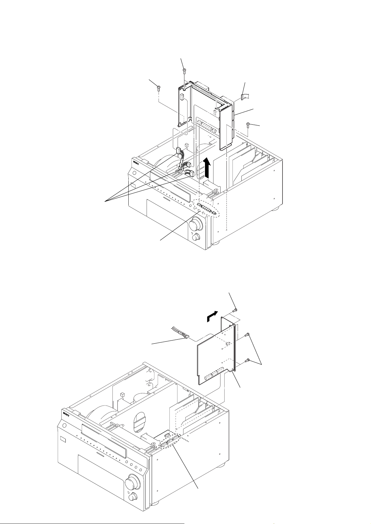
3-4. AMP BOARD BLOCK
7
three connectors
(CN1506, 1512, 1516)
2
screw
(BV3 × 8)
3
two screws
(BV3 × 8)
5
6
connector (CN1503)
8
AMP board
1
screw
(BV3 × 8)
4
three connectors
(CN815, 816, 824)
3-5. COMPONENT BOARD SECTION
5
connector
(CN1306)
1
two screws
(BV/ring)
4
2
four screws
(BV/ring)
6
component board section
14
3
three connectors
(CN819, 820, 821)

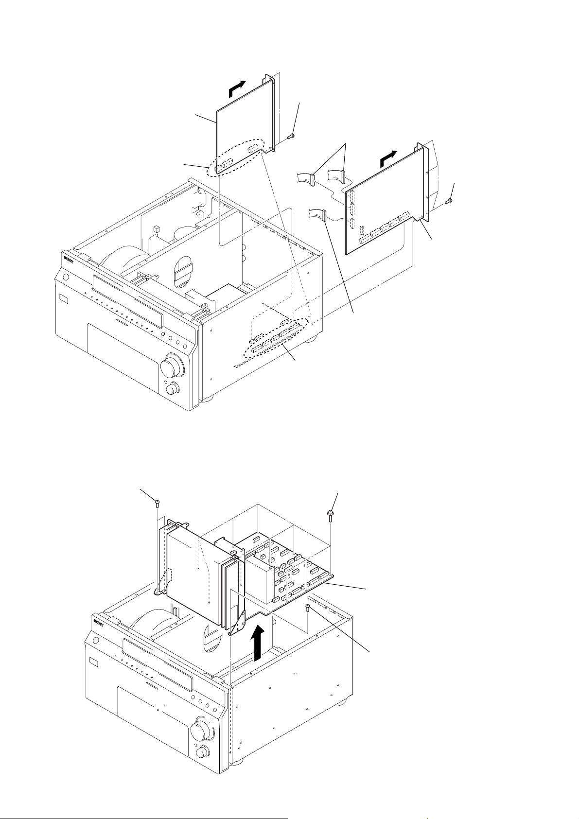
TA-DA9000ES
0
five connectors
(CN101, 102, 103, 104, 105)
qa
main board
9
two screws
(BV/ring)
1
two screws
(BV/ring)
5
SUB board
3
4
connector
(CN1005)
7
connector
(CN1202)
6
two connectors
(CN1201, 1203)
8
preout board
2
four connectors
(CN1001, 1002, 1003, 1006)
3-6. S-VIDEO/VIDEO BOARD BLOCK
3
two connectors
(CN303, 403)
4
S-video/video board block
2
four connectors
(CN815, 816, 817, 818)
1
four screws
(BV/ring)
3-7. SUB BOARD, PREOUT BOARD, MAIN BOARD
15
TA-DA9000ES
3-8. I. LINK BOARD, DIGITAL BOARD
3
I. link board
2
three connectors
(CN3501, 3502, 3503)
1
two screws
(BV/ring)
6
two connectors
(CN2007, 2008)
4
four screws
(BV3
8
digital board section
×
8)
3-9. MOTHER BOARD SECTION
2
two screws
(BV3 × 8)
7
connector (CN2006)
5
five connectors
(CN2001, 2002, 2003, 2004, 2005)
3
ten screws
(transistor)
4
mother board section
16
1
two screws
(BV3 × 8)
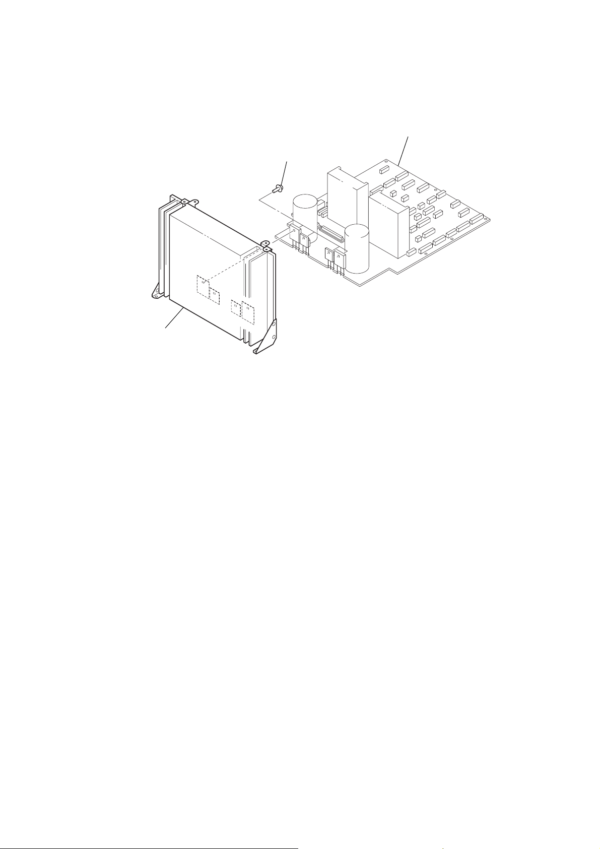
3-10. MOTHER BOARD
1
four screws
(transistor)
3
mother board
TA-DA9000ES
2
heat sink
17

TA-DA9000ES
Ver 1.1
SECTION 4
TEST MODE
TUNER FACTORY PRESET MODE
All preset contents are reset to the default setting.
Procedure:
1. While pressing the [SURR BACK DECODING] and [SLEEP]
buttons, press the I/1 button to turn on the main power.
2. The message “FACTORY PRESET” appears and the present
contents are reset to the default values.
MEMORY CLEARING MODE
All preset contents are cleared when this mode is activated. Use
this mode before returning the product to clients upon completion
of repair.
Procedure:
1. While pressing the [INPUT MODE] and [ENTER] buttons,
press the I/1 button to turn on the main power.
2. The message “MEMORY CLEARING...” appears and the
memories are reset to the default values.
3. When done, the message “MEMORY CLEARED !” appears.
SWAP MODE
Procedure:
1. While pressing the [2CH] and [ENTER] buttons, press
the I/1 button to turn on the main power.
2. The message “SWAP MODE !” appears.
3. Press the [DISPLAY] button.
4. The message “–35.5dB” appears. (Volume level is “MID”)
5. Press the [DISPLAY] button once again.
6. The message “+22.0dB” appears. (Volume level is “MAX”)
7. Press the [DISPLAY] button once again.
8. The message “–oodB” appears. (Volume level is “MIN”)
OPERATION CHECK OF i. LINK TERMINAL
Connect the set to a unit equipped with the i. LINK terminal to
check if the communication can be made correctly . By this operation check, a loose connection of the connector or a disconnection
of the i. LINK cable can be confirmed.
Procedure:
1. Press the I/1 button to turn on the power, and rotate the
[INPUT SELECTOR] knob to set the function to the “i. LINK”
so that the “No LINC” is displayed.
2. Turn on the power of the unit equipped with the i. LINK terminal.
3. Connect the set to the unit equipped with the i. LINK terminal
using the i. LINK cable.
At this time, check that “i. LINK CONNECTING” is displayed
on the set.
4. After the display of “i. LINK CONNECTING”, check that the
equipment information is displayed.
5. Moving the i. LINK cable with the i. LINK connection maintained, check that the “i. LINK CONNECTING” is not displayed.
If nothing is displayed in step 3 and 4, or if “i. LINK CONNECT ING” is displayed continuously, the i. LINK cable will be disconnected or the connector connection will be loose.
If “i. LINK CONNECTING” is displayed in step 5 though the
cable is not removed, the i. LINK cable will be disconnected or
the connector connection will be loose.
FLUORESCENT INDICATOR TUBE PATTERN
CHECK MODE
All fluorescent segments are tested. When this test is acti vated, all
segments turn on at the same time, then each segment turns on one
after another.
Procedure:
1. While pressing the [DISPLAY] and [ENTER] buttons, press
the I/1 button to turn on the main power.
2. All segments and all LEDs turn on.
SOUND FIELD INITIALIZE MODE
The preset sound field is cleared when this mode is activ ated. Use
this mode before returning the product to clients upon completion
of repair.
Procedure:
1. While pressing the [MUSIC] button, press the I/1 button to
turn on the main power.
2. The message “S. F. Initialize” appears and initialization is performed.
COMMAND MODE CHANGE MODE
The command mode of the remote-commander which this set receives can be changed.
Procedure:
1. While pressing the [INPUT MODE] button, press the I/ 1 button to turn on the main power.
2. Either the message “COMMAND MODE [AV1]” or “COMMAND MODE [AV2]” appears. Select the desired mode.
SF LOCK ON/OFF CHANGE MODE
Procedure:
1. While pressing the [MUSIC] and [ENTER] buttons, press
the I/1 button to turn on the main power.
2. Either the message “SF LOCK [OFF]” or “SF LOCK [ON]”
appears.
18
TA-DA9000ES
SPECIAL MENU MODE
Procedure:
1. Press the I/ 1 button to turn on the main power, then while pressing the [ENTER] button, press the [MUSIC], [DIRECT], [MOVIE]
button in order.
2. The message “MENU SPECIALIZED !” appears.
3. Each time the [MENU] dial is turned clockwise, the item is switched in order as follows.
4. To release from this mode, while pressing the [ENTER] button, press the [MUSIC], [DIRECT], [MOVIE] button in order again.
5. The message “MENU SPECIALIZED OFF” appears.
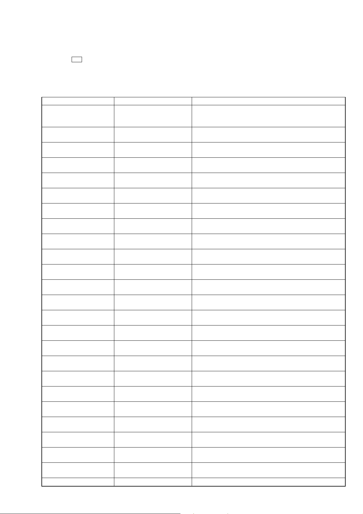
Items Display Remark
Version display SPECIAL ###: distination,
A9ES ### v*.** XXXX XXXX: Sum value of flash memory
in the main microprocessor
Distinatin change SPECIAL
FL display fonts test SPECIAL Not used for the servicing
FL display test ALL ON Each time
Audio swap SPECIAL Switching with
SWAP [XXXXXXXXXXX
DSP reset SPECIAL XXX: ON or OFF (switching with
DSP RESET [XXX
DSP 1 IRAM DSP 1 IRAM Not used for the servicing
DSP 1 ARAM DSP 1 ARAM Not used for the servicing
DSP 2 IRAM DSP 2 IRAM Not used for the servicing
DSP 2 ARAM DSP 2 ARAM Not used for the servicing
DSP 2 ARAM DSP 2 ARAM Not used for the servicing
1st bass gain SPECIAL Not used for the servicing
1st bass frequency SPECIAL Not used for the servicing
2nd bass gain SPECIAL Not used for the servicing
2nd bass frequency SPECIAL Not used for the servicing
Bass select SPECIAL Not used for the servicing
Bass management SPECIAL Not used for the servicing
BASS MAN. [
DSP boot error SPECIAL Not used for the servicing
DSP write 1 error SPECIAL Not used for the servicing
DSP write 2 error SPECIAL Not used for the servicing
DSP write 3 error SPECIAL Not used for the servicing
DSP read 1 error SPECIAL Not used for the servicing
DSP read 2 error SPECIAL Not used for the servicing
DSP read 3 error SPECIAL Not used for the servicing
DSP HALT SPECIAL XXX: ON or OFF (switching with
****
]
]
] XX
: destination, XX: at or fx (switching with [--/+] dial)
****
MODEL [
FL FONT 0x** = [X
AE9S
[DISPLAY] button to change as follows.
all on t test pattern 1 t test pattern 2 t all off t all on
[
I
*****
[
D
*****
[
I
*****
[
D
*****
[
D
*****
1st BASS GAIN X.XdB
1st BASS FREQ XXXHz
2nd BASS GAIN X.XdB
2nd BASS FREQ XXHz
BASS SELECT [1st or 2nd]
DSP BOOT ERROR:XXX
DSP WRT1 ERROR:XXX
DSP WRT2 ERROR:XXX
DSP WRT3 ERROR:XXX
DSP RAD1 ERROR:XXX
DSP RAD2 ERROR:XXX
DSP RAD3 ERROR:XXX
]=
]=
]=
]=
]=
: main microprocessor software version
*.**
]
****
XX
]
[--/+] dial
[--/+] dial)
XXXX
XXXXXXXX
XXXX
XXXXXXXX
XXXXXXXX
[--/+] dial)
19

TA-DA9000ES
Ver 1.2
Items Display Remark
DSP HALT SPECIAL XXX: ON or OFF (switching with
DSP HALT [XXX
DSP Version display SPECIAL XXX: DSP version
Volume value display SPECIAL
(FL/FR) FL
Volume value display SPECIAL
(SL/SR) SL
Volume value display SPECIAL
Volume value display SPECIAL
(SBL/SBR) SBL
EEPROM debug SPECIAL Not used for the servicing
Super reset SPECIAL Not used for the servicing
2nd volume value display SPECIAL XX: 2nd zone volume value (oo to
3rd volume value display SPECIAL XX: 3rd zone volume value (oo to
FL display duty change SPECIAL XXX: Duty value of FL display (0% to 100%)
SDRAM check SPECIAL Check the operation of LIP SYNC
Error count display SPECIAL Not used for the servicing
Version displa y SPECIAL XXX: sub microprocessor software version
958 hats off SPECIAL Not used for the servicing
I.link test mode SPECIAL Not used for the servicing
YUV Y DRIVE SPECIAL Not used for the servicing
YUV U DRIVE SPECIAL Not used for the servicing
YUV V DRIVE SPECIAL Not used for the servicing
Analog direct SPECIAL Not used for the servicing
****
****
(CT/SW) CT
****
EEPROM
SUPER RESET [XXX
2nd VOLUME –XX (switching with [--/+] dial)
3RD VOLUME –XX (switching with [--/+] dial)
DARK OUT DUTY [XXX%
SDRAM CHECK [XXXXX
SCOM ERROR COUNT XXX
Sub Micom Ver. X.XX
958 HATS OFF [SPDIF or PCM]
i.LINK TEST MODE IN?
YUV Y DRIVE [XX]
YUV U DRIVE [XX]
YUV V DRIVE [XX]
ANALOG DIRECT [2Fs or 4FS]
]
DSP V er 1:vXXX,2:vXXX
: Front L-ch volume value,
FR XXXX XXXX: Front R-ch volume value
SR XXXX XXXX: Surround R-ch volume value
SBR XXXX XXXX: Surround back R-ch volume value
[
****
]
XX
]
****
: Surround L-ch volume value,
****
: Center volume value,
****
****
If super reset is performed, “up convert signal level adjustment”
will also be initialized
When EEPROM initialization is required, perform the “memory
clearing mode” (see page 18)
]
(switching with [--/+] dial)
]
XXXXX: PASS (OK) or ERROR (NG)
SW XXXX XXXX: Volume value display
****
: Surround back L-ch volume value,
[--/+] dial)
)
∞
)
∞
20
OSD ADJUSTMENT
r
Connection
TA-DA9000ES
SECTION 5
ELECTRICAL ADJUSTMENTS
frequency counte
COMPONENT board
CN1309 pin 1 or pin
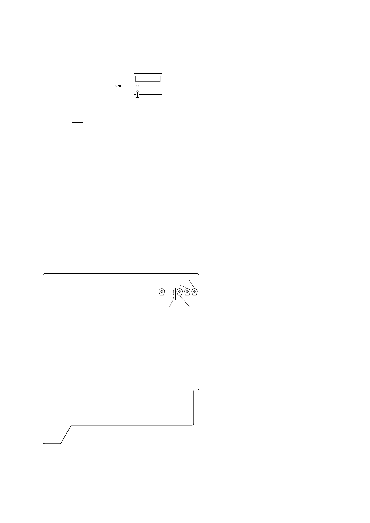
1. Connect a frequency counter to the CN1309 pin 1 on the
COMPONENT board.
2. Press the I/1 button to turn on the main power.
3. Perform the MEMORY CREARING MODE. (See page 17)
4. Press the [ON SCREEN] button on the remote commander (RMLJ312) to display “ON SCREEN [ON]”.
5. Turn the [MAIN MENU] dial to display “<< CUSTOMIZE >>”.
6. Turn the [MENU] dial to display “COLOR SYSTEM”.
7. Turn the [--/+] dial to select PAL.
8. Adjust the CT1304 so that the frequency counter reading is 7.20
MHz.
9. Connect a frequency counter to the CN1309 pin 2 on the
COMPONENT board.
10. Adjust the CT1302 so that the frequency counter reading is
4.433618 MHz ± 50 Hz.
11. Turn the [--/+] dial to select NTSC.
12. Adjust the CT1303 (AEP and UK models) or CT1301 (Taiwan
and Korean models) so that the frequency counter reading is
3.579545 MHz ± 50 Hz.
Note: The steps 5 to 7, 10 and 11 should be performed to AEP and UK
models.
Adjustment and Connection Location:
2
+
–
– COMPONENT BOARD (Component Side) –
CT1302
CT1303
CT1304
4
1
CN1309
CT1301
21
TA-DA9000ES
e
p
e
UP CONVERT SIGNAL LEVEL ADJUSTMENT
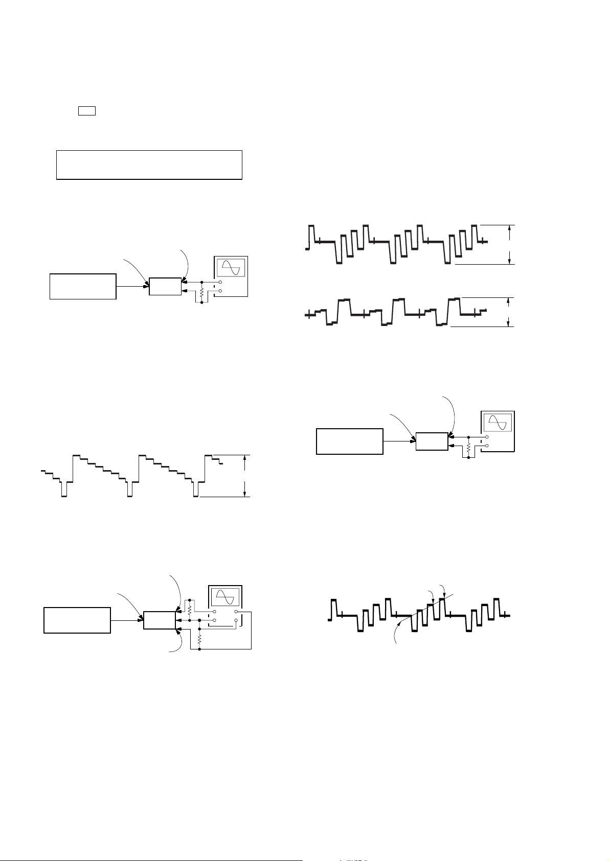
Enter the test mode
1. While pressing the [INPUT MODE] and [DISPLAY] buttons,
press the I/1 button to turn on the main power.
2. It enters the test mode, and display as below figure.
Display
HUE
[7]
1. Y LEVEL ADJUSTMENT
Setting:
S-VIDEO board
VIDEO 1
S2 VIDEO IN jack
(J406)
color pattern
generator
color bars 100%
Procedure:
1. Connect a color pattern generator to the VIDEO 1 S2 VIDEO
IN jack (J406) on the S-VIDEO board, and connect an
oscilloscope to the COMPONENT VIDEO MONITOR OUT
Y jack (J1305) on the COMPONENT board. (75Ω terminated)
2. Enter the test mode.
3. Input color bars signal from the color pattern generator.
4. Adjust the
[MENU] dial so that the Vp-p value of waveform
becomes 1 Vp-p.
Y waveform:
2. COLOR LEVEL ADJUSTMENT
Setting:
S-VIDEO board
VIDEO 1
S2 VIDEO IN jack
(J406)
color pattern
generator
color bars 100%
COMPONENT board
COMPONENT VIDEO
MONITOR OUT
P
R/CR
(J1305)
CONTRAST
[7]
COMPONENT board
COMPONENT
MONITOR OUT
VIDEO Y jack
(J1305)
set
COMPONENT board
COMPONENT VIDEO
MONITOR OUT
P
B/CB
/B-Y jack
(J1305)
75
set
/R-Y jack
COLOR
[7]
75
oscilloscope
Ω
75
Ω
oscilloscop
(AC range)
+
–
Ω
(AC range)
+
–
1 Vp-p
Procedure:
1. Connect a color pattern generator to the VIDEO 1 S2 VIDEO
IN jack (J406) on the S-VIDEO board, and connect an
oscilloscope to the COMPONENT VIDEO PB/CB/B-Y jack and
COMPONENT VIDEO PR/CR/R-Y jack (J1305) on the
COMPONENT board. (75Ω terminated)
2. Enter the test mode.
3. Input color bars signal from the color pattern generator.
4. Display two waveforms of CB and CR simultaneously.
5. Adjust the [--/+] dial so that the Vp-p v alue of wa veforms of C
and CR both may be most set to 0.7V closely.
CB waveform:
0.7 Vp-
CR waveform:
0.7 Vp-p
3. HUE LEVEL ADJUSTMENT
Setting:
COMPONENT board
COMPONENT VIDEO
MONITOR OUT
S-VIDEO board
VIDEO 1
S2 VIDEO IN jack
(J406)
color pattern
generator
color bars 100%
PB/CB/B-Y jack
(J1305)
set
75
Ω
oscilloscop
(AC range)
+
–
Procedure:
1. Connect a color pattern generator to the VIDEO 1 S2 VIDEO
IN jack (J406) on the S-VIDEO board, and connect an
oscilloscope to the COMPONENT VIDEO P
/B-Y jack on
B/CB
the COMPONENT board. (75Ω terminated)
2. Enter the test mode.
3. Input color bars signal from the color pattern generator.
4. Adjust the [MAIN MENU] dial so that the waveform as bellow.
CB waveform:
Adjust so that the height of
A and B may be located in a line
on this line.
B
A
B
22

SECTION 6
DIAGRAMS
6-1. BLOCK DIAGRAM – AUDIO INPUT Section –
VIDEO
AUDIO
AUDIO
MULTI
CHANNEL
IN 1
MULTI
CHANNEL
IN 2
VIDEO 1
IN
VIDEO 2
IN
VIDEO 3
IN
VIDEO 4
IN
LD IN
DVD IN
TV/SAT
IN
PHONO IN
TUNER IN
FRONT
SURROUND
SURR
BACK
FRONT
SURROUND
SURR
BACK
CENTER
SUB
WOOFER
CENTER
SUB
WOOFER
J1006 (1/2)
L
R
J1005 (1/2)
L
R
J1004 (1/2)
L
R
J1003 (1/2)
L
R
L
R
J1002 (1/2)
L
R
L
R
L
R
L
R
L
R
L
R
L
R
L
R
L
R
L
R
J1001
J103
J104
J105
J106
R-CH
R-CH
R-CH
R-CH
R-CH
R-CH
R-CH
R-CH
R-CH
R-CH
R-CH
R-CH
R-CH
R-CH
R-CH
LINE AMP
IC1017
LINE AMP
IC1016
LINE AMP
IC1014
LINE AMP
IC1013
LINE AMP
IC1012
LINE AMP
IC1011
LINE AMP
IC1009
1F-L
1S-L
1SB-L
1SW
2F-L
2S-L
2SB-L
2SW
DVD-L
TV/SAT-L
EQUALIZER
IC1002
LINE AMP
IC1006
1C
2C
V1-L
V2-L
V3-L
V4-L
LD-L
AMP
TAPE-L
MD-L
CD-L
V1-L
V2-L
V3-L
V4-L
V5-L
LC-L
DVD-L
TV/SAT-L
V5-L
PHONO-L
TUNER-L
LINE AMP
IC126
LINE AMP
IC125
LINE AMP
IC124
BUFFER
IC1018
R-CH
R-CH
R-CH
R-CH
INPUT SELECT
2
VIDEO 1
41 VIDEO 1
5 VIDEO 2
38 VIDEO 2
6 VIDEO 3
37 VIDEO 3
7 VIDEO 4
36 VIDEO 4
4 VIDEO 5
39 VIDEO 5
11 CD
32 CD
13 DVD
30 DVD
9 TV/SAT
34 TV/SAT
RY1003
J101 (1/3)
J102 (1/2)
IC1015
J702 (1/2)
V1 26
V2 25
V3 24
MAIN 15
2ND 28
REC IN
27
23
LAT
22
DATA
CLK
21
L
R
RELAY DRIVE
Q1005, 1006
L
R
L
R
L
R
VIDEO 5
TAPE
IN
MD/DAT
IN
CD/SACD
IN
AUDIO
INPUT
MAIN AV L
2ND AV L
LAT927
DATA2
CLK2
RY3
AUDIO
PHONO-L
TUNER-L
CD-L
MD-L
TAPE-L
MAIN AV L
2ND AV L
1S-L
2S-L
1S-BL
2S-BL
1C
2C
1F-L
2F-L
1SW
2SW
INPUT SELECT
IC105
2 PHONO
41 PHONO
4 TUNER
39 TUNER
6 CD/SACD
37 CD/SACD
8 MD/DAT
35 MD/DAT
10 TAPE/CD-R
33 TAPE/CD-R
12 AV IN
31 AV IN
INPUT SELECT
IC102
41 CH1 SL
39 CH2 SL
35 CH1 SBL
34 CH2 SBL
31 CH1 C
30 CH2 C
28 CH1 L
26 CH2 L
12 W
13 W
TAPE
MD
AV OUT
REC OUT 16
REC OUT
DSD 15
MAIN
LAT 23
DATA
CLK
COM L
COM SL
COM SBL 33
COM C 29
COM W
LAT
DATA
CLK
TA-DA9000ES
J1006 (2/2)
L
VIDEO 1
OUT
J1005 (2/2)
J1004 (2/2)
J101 (2/2)
J102 (2/2)
R
VIDEO
AUDIO
L
VIDEO 2
OUT
R
L
VIDEO 3
OUT
R
L
TAPE
OUT
R
AUDIO
L
MD/DAT
OUT
R
AMP
IC112, 123
SBL
W
34
35
9
C
R-CH
R-CH
SL
C
W
8
31
8
39
41
4
2
AUDIO MIX
IC101
LAT 23
DATA
CLK
33
10
29
14
3738
65
22
21
R-CH
LAT1
DATA1
CLK1
MIX AMP
IC107
MIX AMP
IC108
RY3
2QC
S-IN
LAT
CLK 11
OE
RELAY CONTROL
IC1005
• R-CH is omitted due to same as L-CH.
• SIGNAL PATH
: AUDIO (ANALOG)
LEVEL
SHIFT
IC122
LEVEL
SHIFT
IC1001
D/A-L
W
C
SBR
SBL
SR
SL
L
L
SL
SBL
C
W
R-CH D/A-R
W
C
SBR-CH
SBL
SR-CH
SL
R-CH R
SL
SBL
C
W
DATA2
14
LAT
12
CLK2
13
DATA1
CLK1
LAT1
LAT3
DATA2
CLK2
LATVOL
LAT927
2
(Page 27)
3
(Page 29)
4
(Page 24)
LAT-DM
LAT-927X
DATA
LAT-595
CLK
LAT-VOL
OE
5
(Page 25)
R-CH
R-CH
R-CH
R-CH
R-CH
26
25
24
AMP
IC106
27
19
LAT1
DATA1
22
CLK1
21
24
37
14
LAT3
23
DATA1
22
CLK1
21
BUFFER
IC111
BUFFER
IC109
BUFFER
IC127
BUFFER
IC110
2323
TA-DA9000ES
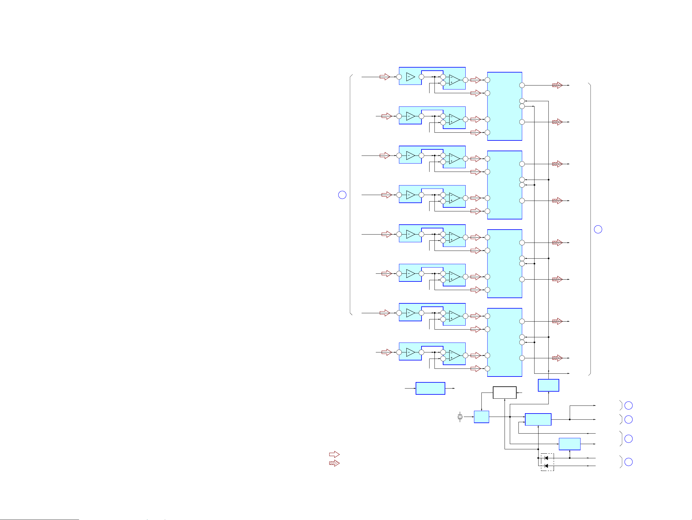
6-2. BLOCK DIAGRAM – A/D CONVERTER Section –
AMP
IC115
6 7 2
3
VREF
6 7 2
VREF
6 7 2
VREF
6 7 2
VREF
6 7 2
VREF
6 7 2
VREF
6 7 2
VREF
6 7 2
VREF
+15V VREF
+5V REGULATOR
IC113
AMP
IC114
3
AMP
IC119
3
AMP
IC118
3
AMP
IC117
3
AMP
IC116
3
AMP
IC121
3
AMP
IC120
3
X2301
22.5792MHz
1
1
1
1
1
1
1
1
IC2304
(Page 23)
L
R-CH
C
W
4
SL
SR-CH
SBL
SBR-CH
OSC
A/D CONVERTER
4 VINL+
5 VINL–
17 VINR+
16 VINR–
A/D CONVERTER
4 VINL+
5 VINL–
17 VINR+
16 VINR–
A/D CONVERTER
4 VINL+
5 VINL–
17 VINR+
16 VINR–
A/D CONVERTER
4 VINL+
5 VINL–
17 VINR+
16 VINR–
B+ SWITCH
Q2302, 2303
IC2011
IC2031
IC2021
IC2041
DSDR
DSDR
11DSDL
9SCKI
10BCK
12DSDR
11DSDL
9DSDL
10BCK
12DSDR
11DSDL
9DSDL
10BCK
12
11DSDL
9DSDL
10BCK
12
D3.3V
CLOCK SELECT
1/2 DIVIDER
IC2306
IC2051
AD-L
AD-R
AD-C
AD-W
AD-SL
AD-SR
AD-SBL
AD-SBR
AD-BCK
(Page 28)
6
I LINK/AD512
I LINK/AD512
7
8
(Page 27)
(Page 28)
• R-CH is omitted due to same as L-CH.
• SIGNAL PATH
: AUDIO (ANALOG)
: AUDIO (DIGITAL)
2424
D2301
SWITCHING
IC2308
I512
22.5792
HATS ON/OFF
595C
10
9
(Page 26)
(Page 25)
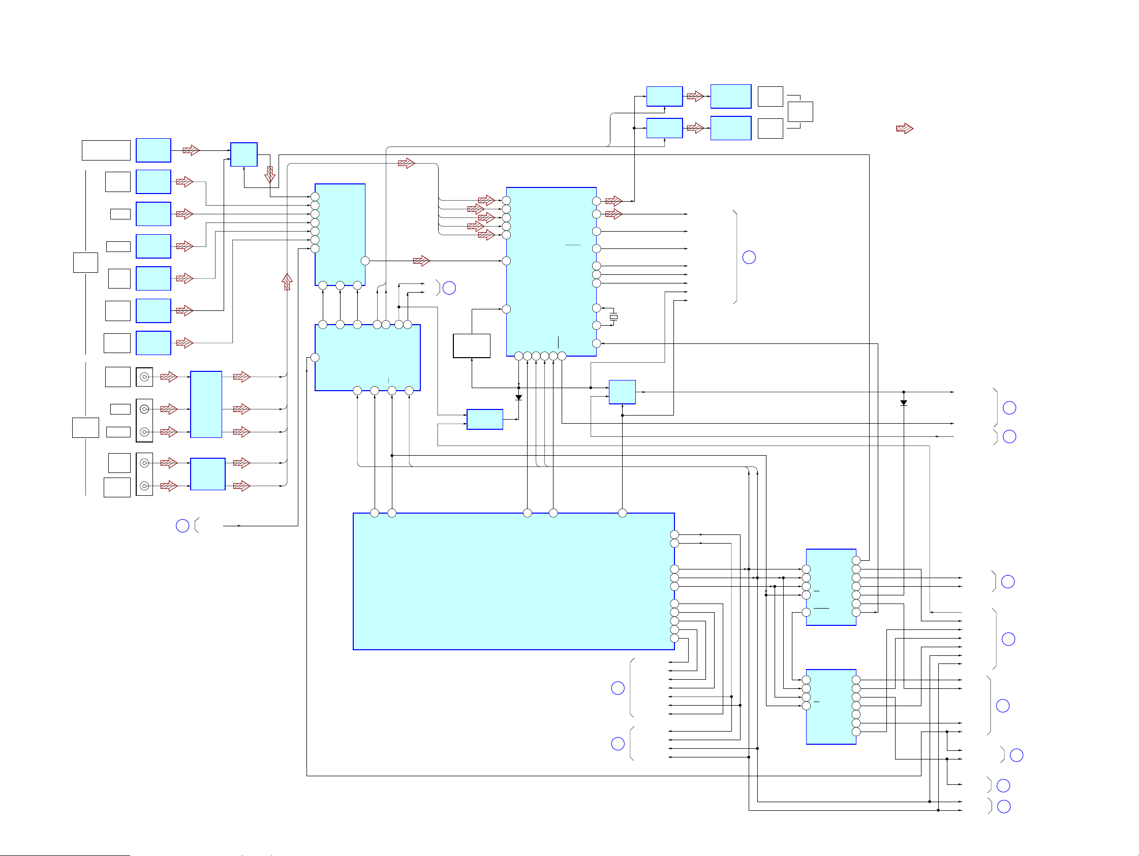
6-3. BLOCK DIAGRAM – DIGITAL INPUT Section –
INPUT SELECT
VIDEO 5 INPUT
DIGITAL OPTICAL
DIGITAL
OPTICAL
DIGITAL
COAXIAL
VIDEO 1
IN
LD IN
DVD IN
TV/SAT
IN
MD/DAT
IN
CD/SACD
IN
VIDEO 1
IN
LD IN
DVD IN
TV/SAT
IN
CD/SACD
IN
OPTICAL
RECEIVER
IC707
OPTICAL
RECEIVER
IC2082
OPTICAL
RECEIVER
IC2084
OPTICAL
RECEIVER
IC2085
OPTICAL
RECEIVER
IC2086
OPTICAL
RECEIVER
IC2087
OPTICAL
RECEIVER
IC2088
J2080
J2081
J2082
(Page 26)
11
WAVE
SHAPER
IC2091
WAVE
SHAPER
IC2092
958OUT
IC2095
B
A
Y
14 D5
15 D4
1D3
2D2
3D1
4D0
12 D7
2QR
VIDEO1
LD
DVD
TV/SAT
CD/SACD
INPUT SELECT
IC2093
A1
A0
10
11
6QG5
QF
5Y
A2
9
QE
7
QE
QH
DIGITAL
INPUT/OUTPUT
CONTROL
IC2451
CLK12LAT13OE
11
COM1-CLK
D-SEL-LAT
34
D595-LAT1
QD
3QD4
D-595OE
33
1
15
QA
14
COM1-DAT
D595-OE
TA-DA9000ES
SWITCHING
Y
COM2-DAT 38
COM2-CLK 39
COM1 DAT 37
COM2 CLK 36
D595-LAT2 35
RY595-LAT
D. MIX LAT 47
RY595-OEOE40
SVOL LAT 48
LAT-VOL
LAT-DM
LAT-927X
LAT-595
COM2-CLK
COM2-DAT
COM1-CLK
COM1-DAT
IC2089
SWITCHING
IC2090
FUN LAT
CLK
DATA
D. SD
DIR-RMCK
DIR-AUDIO
DIR-BCK
DIR-LRCK
DIR-MCK
DIR-RERR
ERR/AUD SEL
42
46
QE
QD
DIGITAL AUDIO
INTERFACE RECEIVER
IC2121
VIDEO1
LD
DVD
TV/SAT
CD/SACD
A
(Page 27)
12
B
QB
S-IN
PLL CLOCK
SELECT
Q2122, 2123
SWITCHING
IC2211
4 RX2
5 RX3
8 RX4
9 RX5/VI
10 RX6/UI
2 RX0
13 LPF
RERR
D2201
MAIN SYSTEM
CONTROLLER
IC2601 (1/4)
21
DIR-DO
39CE40CL38DI37DO36
COM1-DAT
COM1-CLK
20
CKST
34
DIR-CE
XIN 29
XOUT 28
XMODE 41
(Page 23)
(Page 33)
1RXOUT
21RDATA
16RMCK
33AUDIO/V0
17RBCK
20RLRCK
27XMCK
X2121
24.576MHz
SWITCHING
IC2602
A
B
104
ERR/AUD-SEL
5
44
OPTICAL
TRANSCEIVER
IC2081
OPTICAL
TRANSCEIVER
IC2083
VIDEO 1
MD/DAT
(Page 27)
13
COM1-CLK
COM1-DAT
OUT
OUT
DIGITAL
OPTICAL
14 S-IN
11 CLK
12 LAT
13 OE
14 S-IN
11 CLK
12 LAT
13 OE
DATA DECODER
IC2461
9 S-OUT
DATA DECODER
IC2462
QA
QB
QC 2
QD
QF
QG
QH
QB 1
QC
QD
QE
QF
QG
QH
• R-CH is omitted due to same as L-CH.
• SIGNAL PATH
: AUDIO (DIGITAL)
DIR ERR
D2602
DIR CKST
ERROR-3210
15
1
3
5
6
7
2
3
4
5
6
7
V POWER
I POWER
CLKSEL
SELFS1
SELFS2
SELCF1
SELCF2
COM1-CLK
COM1-DAT
TA-RST
SWAP1
SWAP2
595C
595C
HATS ON/OFF
18
14
15
16
17
(Page 28)
(Page 26)
(Page 34)
(Page 28)
(Page 28)
(Page 24)
10
I512 OFF
CLK
DATA
19
20
(Page 26)
(Page 32)
2525

TA-DA9000ES
6-4. BLOCK DIAGRAM – I. LINK Section –
J3002
i. LINK S200
AUDIO IN
TAIP
TAIN
TBIP
TBIN
4
3
2
1
BIAS
14
TRA1P
143
TRA1N
142
TRB1P
141
TRB1N
145
DI1O
DI2O
DI5O
DI6O
DI3O
DI4O
VALIB OUT
ERR_OUT
SYTOUT
DIVIDER
IC3009
QC
15
16
19
20
17
18
3
174
24
DSD-L
DSD-R
DSD-SL
DSD-SR
DSD-C
DSD-W
64FS
22
(Page 28)
SWITCHING
IC3007 (1/2)
1 CLR
2CK
1 CLR
2CK
LOAD
DIVIDER
IC3006
LOAD
ENT
ENP
C0
ENP
12
10
15
9
7
9
7
IC3007 (2/2)
• SIGNAL PATH
ERROR-3210
: AUDIO (DIGITAL)
ERROR-3210
15
(Page 25)
(Page 25)
(Page 24)
21
(Page 27)
11
9
I512
DATA
MILES AUDIO
MILES RESET
LEVEL SHIFT
IC3013
164
27
167
171
172
DOUT958OUT
FSS12 OUT
FSS1222.5792
SACKOBCK
LRCKOLRCK
I. LINK INTERFACE
IC3003
XRAS
XCAS
XWE
XOE
XRD
XWR
XCS
XRDY
PWD
XRESETO
XRESETL
47 – 40, 38 – 31
DATA0 – DATA15
55 – 62
ADDRESS8
ADDRESS1 –
129
XO
XI
130
90 – 83
99 – 92,
DT0 – DT15
69 – 66
A0 – A9
76 – 71,
78
79
81
80
52
51
50
53
119
122
165
X3001
24.576MHz
SD-RAM
IC3008
D0 – D15
2 – 5, 7 – 10,
41 – 44, 46 – 49
27 – 32
A0 – A9
21 – 24,
18
XRAS
34
UCAS
35
LCAS
17
XWE
33
XOE
D0 – D15 D0 – D15
A1 – A8
EEPROM
IC3001
D0 – D7
15 – 19
D0 – D7
11 – 13,
25 – 23
A0 – A12
10 – 2, 21,
20 48CE EEP_CS
OE RD
22 44
27
WE
VCO
IC3005
DATA BUS
A1 – A13
A1 – A13
ADDRESS BUS
35 ERR CLR
88 – 73
D0 – D15
61 – 57
A1 – A13
71 – 65, 63,
46 WR
18 MIES AUDIO
49
CXD3270_XCS
39
RDY
89
PHY_BIAS
90
PHY_RST
92
LINK_RST
I. LINK SYSTEM
CONTROLLER
IC3002
UN-MUTE
XOUT
XIN
10
7 – 1, 100
HD0 – HD7
51HCNTL0
52HCNTL1
19AKE_XF
21HRDY
22XHAS
23XHDS1
24XHDS2
25XHCS
26XRS
54HRW
53HBIL
30IIC DATA
29IIC CLK
12RESET
13
15
58, 69, 81, 95,
39 HCNTL0
46 HCNTL1
27 XF
55 HRDY
13 HAS
127 HDS1
129 HDS2
17 HCS
98 RS
18 HR/W
62 HBIL
RESET SWITCH
IC3011
X3002
10MHz
HD0 – HD7
120, 124, 135, 6
I. LINK DSP
IC3012
X2/CLKIN
96
X1
X3003
20MHz
97
I2C-DATA
I2C-CLK
23
(Page 33)
19
(Page 25)
I512 OFF
REFOUT
PLLCKI
4FINA
23
25
5FINB
3 VCOO
10VCOX
2626
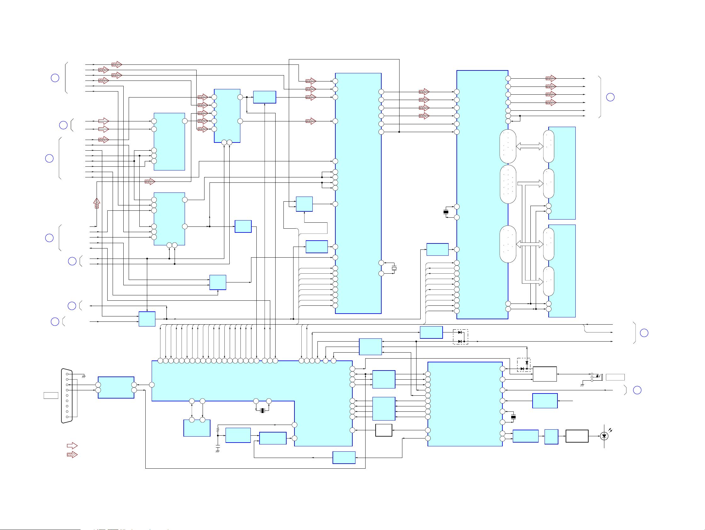
6-5. BLOCK DIAGRAM – DSP Section –
TA-DA9000ES
(Page 28)
13
(Page 25)
21
(Page 26)
(Page 24)
RS232C
24
2
(Page 23)
ERR/AUD SEL
(Page 28)
7
J3501
1
2
3
4
5
6
7
8
9
F2 SBLR
F2 FLFR
F2 CSW
F2 SLSR
F2 LRCK
F2 BCK
D/A-R
D. SD
DIR-AUDIO
DIR-RMCK
DIR-LRCK
DIR-BCK
DIR-MCK
DIR-RERR
DATA
BCK
LRCK
MILES AUDIO
MILES RESET
A
12
MCK
25
I LINK/AD512
B
TXD
DTR
(Page 25)
• SIGNAL PATH
: AUDIO (ANALOG)
: AUDIO (DIGITAL)
RS-232C DRIVER
IC3501
T1OUT
17
16 R1IN
DSP1
IC2201
DIGITAL AUDIO SELECT
IC2208
6 1C0
2XRST
12
2XRST
1HACN
11
SCL
114
6
SCL
5 1C1
3 1C3
10
11 2C1
SWITCHING
IC2204
A
B
1HCS
1HDOUT
10
8
1HACN
1HDOUT
2C0
S
1BST
7
1HCS
1BST
A
B
214
Y
1PM
1GP9
6
5
1PM
1GP9
RESET SIGNAL
BUFFER
IC2604
1XRST
4
1XRST
A/D CONVERTER
IC2001
IC2205
2HACN
17
2HACN
A
B
214
2HCS
2HDOUT
16
2HCS
2HDOUT
2BST
15
12DOUTD/A-L
71Y
92Y
2BST
2GP3
14
2GP3
2PM
13
2PM
SDA
113
5
SDA
EEPROM
IC2603
1
2 VINR
11 BCK
10 LRCK
15 SCKI
CLOCK SELECT
6 1C0
5 1C1
3 1C3
2C0
10
11 2C1
13 2C3
S
A
Y
B
CLOCK
SELECT
IC2307
2EXLOCK
19
18
2EXLOCK
109 SOUT1
13T1IN
15R1OUT
71Y
92Y
BUFFER
IC2210
1BST SEL
3
1BST SEL
DSP CLK
DSP HDIN
2
1
89
DSP CLK
DSP HDIN
57
SWITCHING
IC2209
125
72
FSRATE
PCM-SEL
X1
58
X2601
16.5MHz
RESET SWITCH
IC2605
SWITCHING
IC2207
A
B
IBST
IBST SEL
1HACN
1HDOUT
1GP9
1PM
1XRST
DSP HDIN
DSP CLK
1HCS
STOP
23
ILINK RST
DIR-DTAAO
MAIN SYSTEM CONTROLLER
X0
78
STOP
IC2601 (2/4)
69 RST TRG
55 RSTX
Y
S
LEVEL SHIFT
IC2203
POW RY2
75
76
POW RY
POW RY2
115 S D I 4
114 S D I 3
30 SDI2
18 SDI1VINL
59 EXLOCK
17 BCKI1
29 BCKI2
28 LRCKI2
15 LRCKI1
56 BST
22 KFSIO
69 GP8
32 HACN
35 HDOUT
68 GP9
112 P M
2 XRST
33 HDIN
34 HCLK
36 HCS
52
60
54
MD2
A1IN
51A1 OUT
MD0
110SIN1
70END-FLAG
71A1-LAT
50MBUS-STS0
64MBUS-STS1
65MBUS-STS2
66MBUS-STS3 42 STAT3
67MBUS-STS4 41 STAT4
BUFFER
IC2703 (2/3)
BUFFER
IC2703 (1/3)
IC2704 (2/2)
23SDO1
24SDO2
25SDO3
26SDO4
20BCKO
19LRCKO
9MCLK1
12MCLK2
BUFFER
BUFFER
IC2702
BUFFER
Q2703
X2201
13.5MHz
LEVEL SHIFT
IC2254
2EXLOCK
2HACN
2HDOUT
2HCS
2BST
2GP3
2PM
2XRST
DSP HDIN
DSP CLK
BUFFER
IC2704 (1/2)
26 URTIN
25 ENDFLG
5 CTRL-LATCH
23 OUTHI2
24 OUTLO2
1 STAT0
44 STAT1
43 STAT2
19 RESETC
X2251
13.5MHz
27 SDI1
28 SDI2
35 SDI3
39 SDI4
38 BCKI1
29 LRCKI1
144 MCLK1
139 MCLK2
62 KFSIO
136 EXLOCK
83 HACN
82 HDOUT
76 HCS
141 B S T
120 G P 3
140 P M
8 XRST
74 HDIN
75 HCLK
D2603
SUB SYSTEM
CONTROLLER
IC2701
DSP2
IC2251
D16 – 31
A0 – 15
D0 – 15
SDO1
60
SDO2
61
SDO3
25
BCKO
64
LRCKO
111
GP7
79 68 67 58 – 56
122 114 113 106 105
129 128 125 – 123
85WEO
84CSO
12A1-IN
11A1-OUT
10SIRCS_INPUT
14RESET
15XIN
16XOUT
2CARRIER-OUT
33SIRCS-OUT
31 22 – 20
53 – 51 44 43 32
59 50 42 41 34
95 86 78 77 70 69
116 115 104 103
94 – 92 89 – 87 80
D2701
X2701
7.28MHz
SIRCS SWITCH
IC2705
7 – 10 13 – 16
44 – 42 27 – 24
17 WE
6CE
7 – 10 13 – 16
44 – 42 27 – 24
17 WE
6CE
CONTROL A1
INTERFACE
Q2701, 2702
RESET SIGNAL
GENERATOR
IC2706
LEVEL
SHIFT
IC704
D0 – 15
29 – 32 35 36
A0 – 15
21 – 18 5 – 1
D0 – 15
29 – 32 35 36
A0 – 15
21 – 18 5 – 1
S-RAM
IC2252
S-RAM
IC2253
D+5V
LED DRIVE
Q701 – 703
SD01
SD02
SD03
SD0426SDO4
BCK
LRCK63
STOP
ROW-RY2
26
(Page 28)
J3533
CTRL A1
STOP
ROW-RY2
POW-RY1
II
SIRCS
(Page 33)
D710 – 713,
D716, 717
(IR RECEPTER)
27
(Page 34)
28
2727
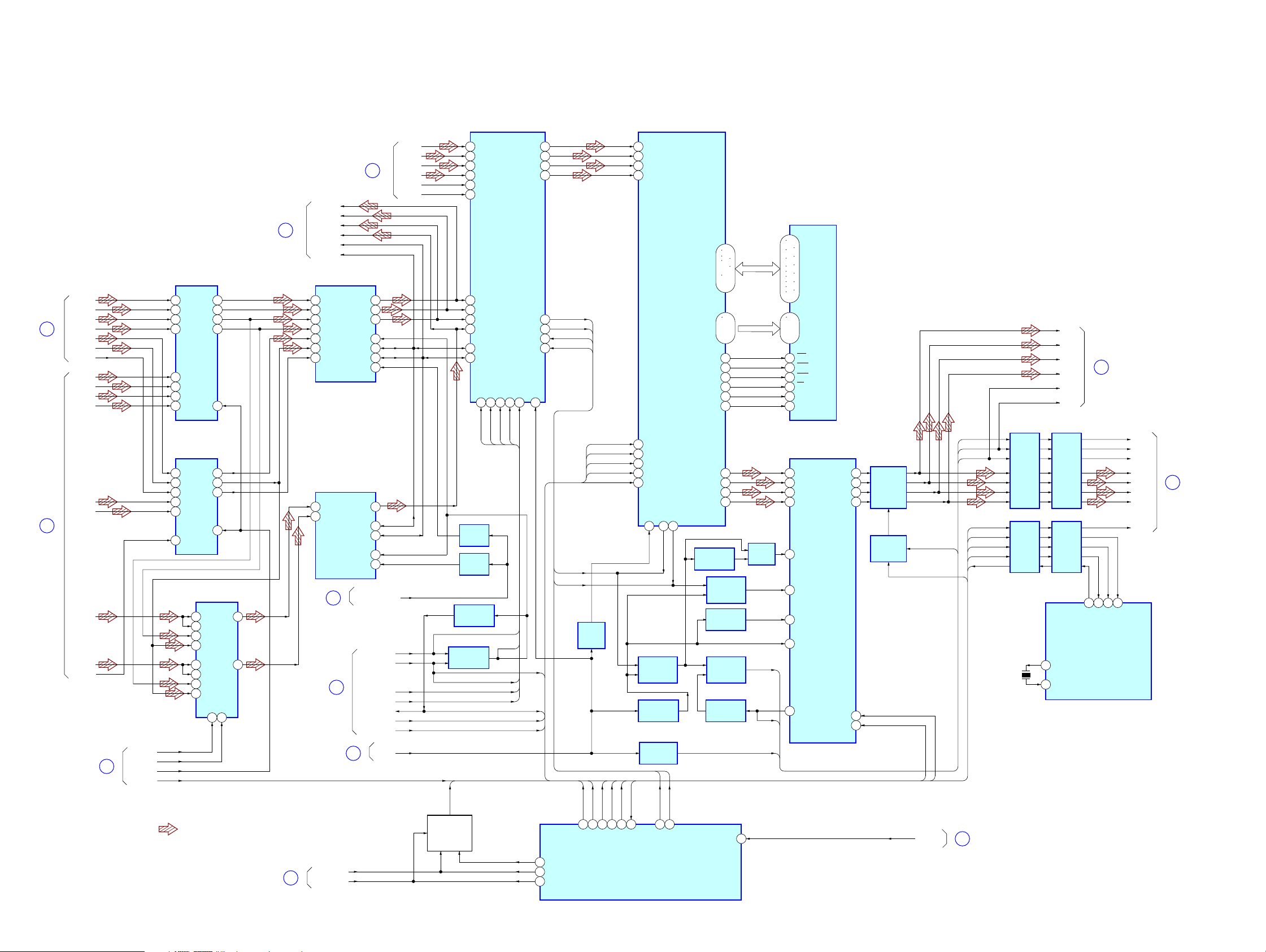
TA-DA9000ES
6-6. BLOCK DIAGRAM – DIGITAL AUDIO Section –
22
(Page 26)
6
(Page 24)
DSD-L
DSD-R
DSD-SL
DSD-SR
DSD-C
DSD-W
64FS
AD-L
AD-R
AD-SL
AD-SR
AD-C
AD-W
AD-SBL
AD-SBR
AD-BCK
18
(Page 25)
SWAP1
SWAP2
595C
TA-RST
DSD SELECT
IC2063
2A0
5A1
11 A2
14 A3
3B0
6B1
10 B2
13 B3
DSD SELECT
IC2064
2A0
5A1
11 A2
3B0
6B1
10 B2
DSD SELECT
IC2052
10 1C0
11 1C1
12 1C2
13 1C3
62C0
52C1
42C2
32C3
DC CUT
DIGITAL FILTER
IC2401
SDO1
SDO2
SDO3
26
(Page 27)
F2 FLFR
F2 CSW
24
(Page 27)
4Y0
7Y1
9Y2
12Y3
1S
4Y0
7Y1
9Y2
1S
91Y
72Y
F2 SLSR
F2 SBLR
F2 BCK
F2 LRCK
DSD/PCM CONVERTER
IC2161
39 DSIFL
40 DSIFR
41 DSICT
42 DSISW
43 DSISL
44 DSISR
38 DSBCK
DSD/PCM CONVERTER
IC2163
39 DSIFL
40 DSIFR
I LINK/AD512
8
(Page 24)
17
AB
142
(Page 25)
COM1-CLK
COM1-DAT
25
(Page 27)
SDO4
BCK
LRCK
23POFLR
22POCSW
21POSLR
3SEL4FS
19PBCK
20PLRCK
27MCK
23POFLR
19PBCK
20PLRCK
3SEL4FS
27MCK
SELFS1
SELFS2
SELCF1
SELCF2
CLKSEL
MCK
TA-XRST
32 PIA12
33 PIA34
34 PIA56
35 PIA78
29 PA BCK
30 PA WCK
41 PIB12
42 PIB34
43 PIB56
44 PIB78
38 PBBCK
39 PBMCK
BUFFER
IC2162
BUFFER
IC2164
BUFFER
IC2428 (3/5)
SWITCHING
IC2402
45
PID
SELCF2
SELPID
5
SCF2
SELCF1
4
SCF1
SFS1
PID
FS
SFS2
SCF1
SCF2
SELFS2
2
3
SFS2
SFS1
CLKSEL
CLK
DAT
SELFS1
27
MCK
20PIO12
21PIO34
22PIO56
23PIO78
P0BCK
17P0BCK
P0WCK
18P0WCK
INIT
47INIT
BBSEL
11BBSEL
CLK
DAT
TA-SO
TA-XCS
TA-XRST
P0WCK
P0BCK
LEVEL
SHIFT
IC2303
LIP SYNC ADJUST
66 FLFRI
65 SLSRI
64 CSWI
63 DLDRI
72 SCLK
74 SI
75 SO
73 XCS
70 XRST
CK51259LRCKI60BCKI
68
SHIFT
REGISTER
IC2429 (1/2)
BUFFER
IC2428 (1/5)
1/2 DIVIDER
IC2305
IC2301
D0 – 15
A0 – 11
BUFFER
IC2428 (5/5)
IC2429 (2/2)
IC2428 (2/5)
IC2428 (4/5)
100 1 – 5 7 8
17 – 22
10WE
11CAS
12RAS
13CS
14CLK
15CKE
47FLFRO
46SLSRO
45CSWO
44BL_BRD
SHIFT
REGISTER
BUFFER
SHIFT
REGISTER
IC2430
BUFFER
90 – 95 97 98
24 – 29
DELAY
IC2427
LRCKO
BCKO
MCK1
DQ0 – 15
2 3 5 6 8 9 11 12 39
40 42 43 45 46 48 49
A0 – 11
19 – 24
27 – 32
15 WE
16 CAS
17 RAS
18 CS
35 CLK
34 CKE
35 DATA_1
36 DATA_2
37 DATA_3
38 DATA_4
PROGRAMMABLE
LOGIC DEVICE
IC2426
1 EDGE
2 BCKIN
3 BCK2IN
5 MCK
12 MCKOUT
SD-RAM
IC2302
22DIOUT_1
21DIOUT_2
20DIOUT_3
19DIOUT_4
32CLKSEL
33FS
MUTING
IC2511
MUTING
CONTROL
IC2512
FS
LRCKO
MUTE
CLKSEL
MCK1
BCKO
LRCKO
RESET
MUTE
U-MAIN
U-SUB1
U-SUB2
X1501
8MHz
BUFFER
IC2501
BUFFER
IC2503
D01
D02
D03
D04
LRCK
BCK
BUFFER
IC2504
BUFFER
IC2506
OUTPUT CONTROLLER
23 X1
22 X0
29
(Page 29)
60
U-SUB242U-SUB114U-MAIN
IC1800 (1/2)
64
MUTE
MCK1
BCKO
LRCKO
DATA1
DATA2
DATA3
DATA4
RESET
30
(Page 30)
• SIGNAL PATH
: AUDIO (DIGITAL)
14
(Page 25)
DIR ERR
DIR CKST
MUTE
SYSTEM
MUTING
SWICTH
Q2601 – 2603
84 S-MUTE
22 DIR-ERROR
24 DIR-CKST
TA-XCS
29
TA-XCS
TA-SO
30
TA-SO
RESET
83
85
SUB-RST
U-MAIN
U-SUB1
87
MAIN CLK
U-SUB2
86
SUB DATA
MAIN DATA
2828
INIT
BBSEL
25
88
9776-INIT
BBSEL
MAIN SYSTEM
CONTROLLER
IC2601 (3/4)
115HP IN
HP SW
31
(Page 29)
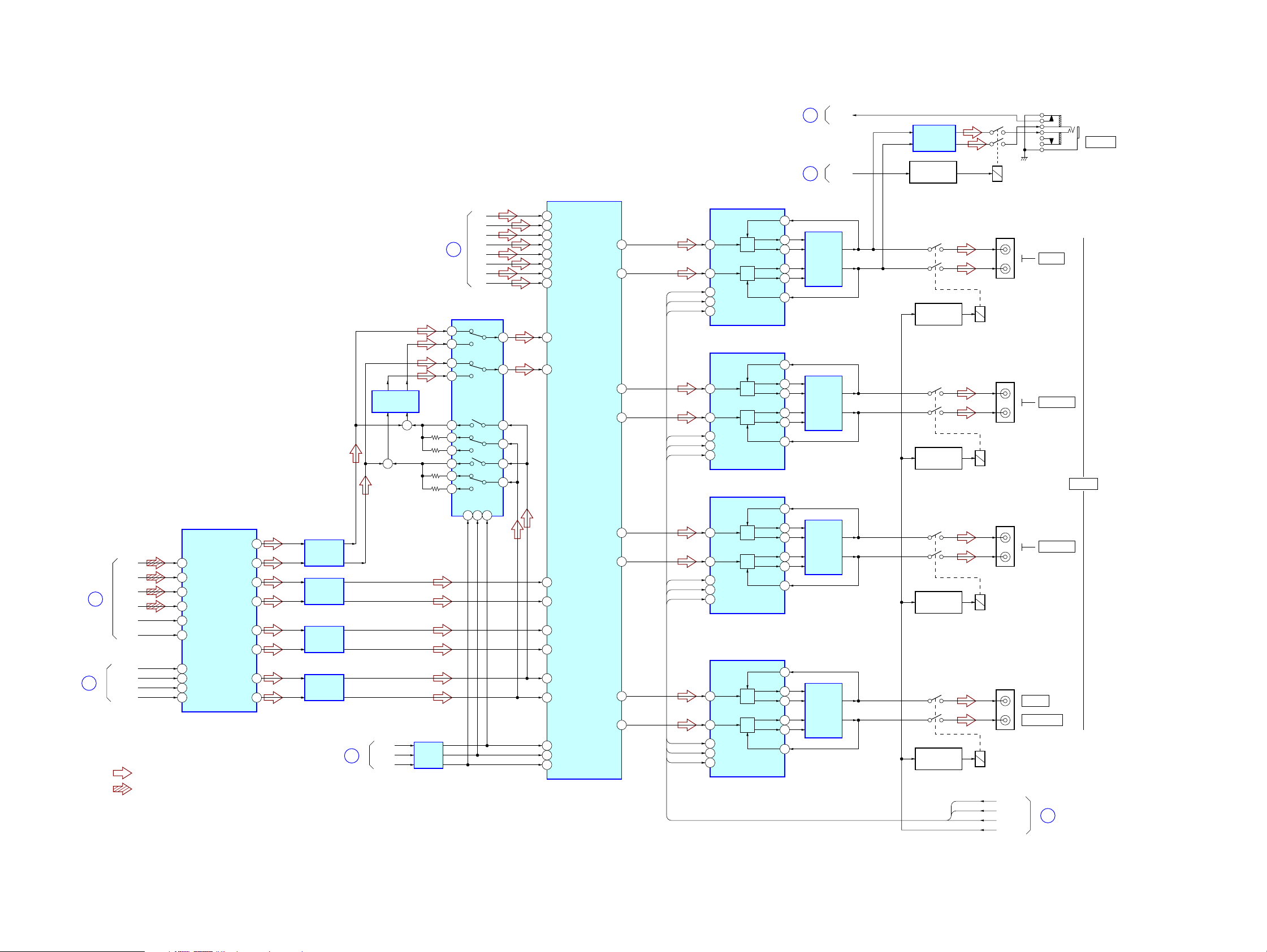
6-7. BLOCK DIAGRAM – AUDIO OUTPUT Section –
31
(Page 28)
HP SW
HEADPHONE
AMP
IC1315
TA-DA9000ES
J701
PHONES
29
(Page 28)
32
(Page 33)
• SIGNAL PATH
: AUDIO (ANALOG)
: AUDIO (DIGITAL)
DATA145D01
DATA246D02
DATA347D03
DATA431D04
BCK40BCK
LRCK41LRCK
MDI34DA-DAT
MC35DA-CLK
MDO33DA-OUT
ML36DA-LAT
D/A CONVERTER
IC2901
VOUT1
VOUT2
VOUT3
VOUT4
VOUT7
VOUT8
VOUT5
VOUT6
HP RY
23
24
25
23
24
25
23
24
25
23
24
25
4
6
5
4
6
5
4
6
5
4
6
5
35
(Page 32)
LINE AMP
IC1314
LINE AMP
IC1308
LINE AMP
IC1306
LINE AMP
IC1303
AUDIO SELECT
SWITCH
IC1205
ANA L28
34
ANA R15
ANA SL41
ANA SR2
ANA SBL35
ANA SBR8
ANA C31
ANA W12
DIGI L26
DIGI R1725
DIGI SL39
DIGI SB4
DIGI SBL
DIGI SBR9
DIGI C30
DIGI W13
DATA22
LAT23
CLK24
COM LL24
COM R 19
DATA
CLK
VOL-LAT
COM SL 37
COM SR 6
DATA
CLK
VOL-LAT
COM SBL 33
COM SBR 10
DATA
CLK
VOL-LAT
COM C 29
COM W 14
DATA
CLK
VOL-LAT
R
SL
(Page 23)
MIX AMP
IC1203, 1204
+
+
L
14
13
12
11
16
20
10
9
R
SL
SR
SBL
SBR
C
W
LOW-PASS
FILTER
IC1206
LOW-PASS
FILTER
IC1207
LOW-PASS
FILTER
IC1209
LOW-PASS
FILTER
IC1208
33
(Page 33)
DATA
LAT
CLK
LEVEL
SHIFT
IC1201
3
3
2
26
27
5
6
21
23
24
SR
SBL
SBR
C
W
SWITCHING
IC1202
LA
CLK
1614 15
4
128
7
17
22
DA
ELECTRICAL VOLUME
IC1313
M-IN
9
M-IN
20
16 DATA
13 CK
17 STB
ELECTRICAL VOLUME
IC1307
M-IN
9
M-IN
20
16 DATA
13 CK
17 STB
ELECTRICAL VOLUME
IC1305
M-IN
9
M-IN
20
16 DATA
13 CK
17 STB
ELECTRICAL VOLUME
IC1302
M-IN
9
M-IN
20
16 DATA
13 CK
17 STB
T-IN
M-OUT
T-OUT
M-OUT
T-OUT
T-IN
T-IN
M-OUT
T-OUT
M-OUT
T-OUT
T-IN
T-IN
M-OUT
T-OUT
M-OUT
T-OUT
T-IN
T-IN
M-OUT
T-OUT
M-OUT
T-OUT
T-IN
RELAY DRIVE
Q1305
RELAY DRIVE
Q1304
RELAY DRIVE
Q1303
RELAY DRIVE
Q1302
RELAY DRIVE
Q1301
DATA
CLK
VOL-LAT
RY1305
J1304 (1/2)
RY1304
J1304 (2/2)
RY1303
J1303 (1/2)
RY1302
J1303 (2/2)
RY1301
DATA
CLK
VOL-LAT
PRE OUT
(L)
(R)
(L)
(R)
(L)
(R)
CENTER
SUB WOOFER
(Page 32)
FRONT
SURROUND
PRE OUT
SURR BACK
34
2929
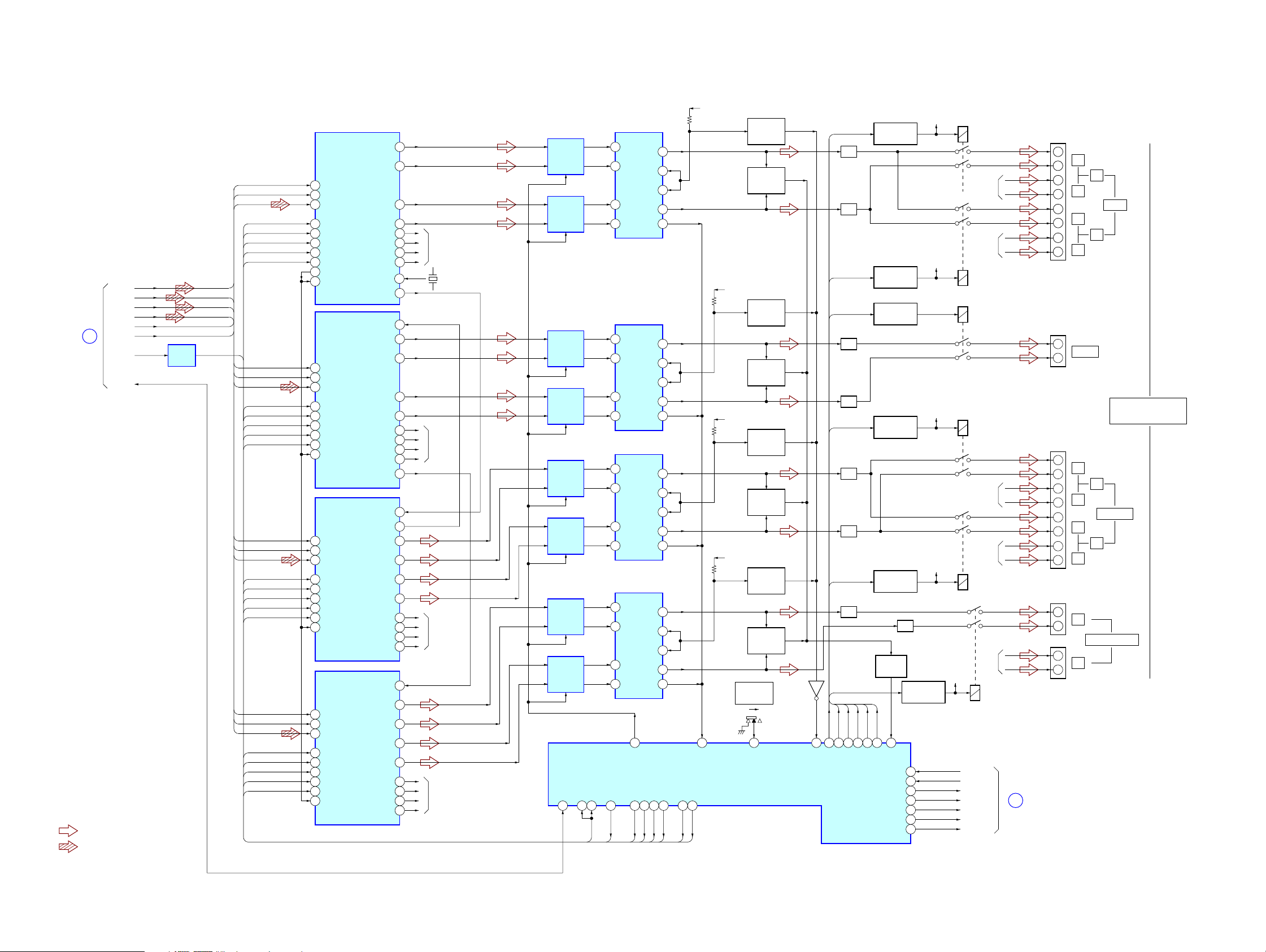
TA-DA9000ES
6-8. BLOCK DIAGRAM – POWER AMP Section –
LRCK
BCK
DATA1
INIT
SCDT
SHIFT
LAT1
SCK
DATA1
DATA2
DATA3
DATA4
LRCKO
30
BCKO
MCK1
RESET
BUFFER
IC1531
(Page 28)
• R-CH is omitted due to same as L-CH.
• SIGNAL PATH
: AUDIO (ANALOG)
: AUDIO (DIGITAL)
DATA1
DATA2
DATA3
DATA4
LRCK
BCK
SCK
LRCK
BCK
DATA3
INIT
SCDT
SHIFT
LAT3
SCK
LRCK
BCK
DATA2
INIT
SCDT
SHIFT
LAT2
SCK
LRCK
BCK
DATA4
INIT
SCDT
SHIFT
LAT4
SCK
PCM/PWM
PROCESSOR
IC1505
45 LRCK
44 BCK
43 DATA
41 INIT
38 SCDT
37 SCSHIFT
36 SCLATCH
64 XFSIIN
73 FSOCLK
74 FSOI
PCM/PWM
PROCESSOR
IC1504
45 LRCK
44 BCK
43 DATA
41 INIT
38 SCDT
37 SCSHIFT
36 SCLATCH
64 XFSIIN
74 FSOI
PCM/PWM
PROCESSOR
IC1517
45 LRCK
44 BCK
43 DATA
41 INIT
38 SCDT
37 SCSHIFT
36 SCLATCH
64 XFSIIN
74 FSOI
PCM/PWM
PROCESSOR
IC1516
45 LRCK
44 BCK
43 DATA
41 INIT
38 SCDT
37 SCSHIFT
36 SCLATCH
64 XFSIIN
74 FSOI
OUT R1–
XFSO IN
OUT R1–
OUT R1–
OUT R1–
+V1
LPF
RELAY DRIVE
Q615
15AC-OFF
3TEMP
344/8 OUT
26VOL-DATA
25VOL-CLK
27VOL-LAT
28DAC-MUTE
R-CH
R-CH
R-CH
R-CH
R-CH
RY603
R-CH
R-CH
RY601
RY605
RY607
R-CH
R-CH
RY606
R-CH
AC OFF
TEMP
4/8 RY
VOL DATA
VOL CLK
VOL LAT
D/A MUTE
RY610
36
(Page 34)
TM601
+
−
+
−
+
−
+
−
TM603 (1/2)
+
−
TM602
+
−
+
−
+
−
+
−
TM604
+
−
TM603 (2/2)
+
−
L
A
R
L
B
R
CENTER
L
A
R
SURROUND
L
B
R
L
SURROUND BACK
R
FRONT
SPEAKERS
IMPEDANCE USE 4 – 16Ω
A+B USE 8 – 16Ω
CURRENT
LIMITER
+V1
+V2
+V2
S601
IMPEDANCE
SELECTOR
4Ω 8Ω
Q1505
OVER LOAD
DETECT
Q601, 602
CURRENT
LIMITER
Q1503
OVER LOAD
DETECT
Q605, 606
CURRENT
LIMITER
Q1509
OVER LOAD
DETECT
Q607, 608
CURRENT
LIMITER
Q1507
OVER LOAD
DETECT
Q611, 612
4I-LIMIT
Q1513
18OUT L2+
15OUT L2–
24OUT L1+
21OUT L1–
10OUT R1+
7
1OUT R2+
4OUT R2–
28
77XFSOUT
28XFSO IN
15OUT L2+
18OUT L2–
24OUT L1+
21OUT L1–
10OUT R1+
7
1OUT R2+
4OUT R2–
77XFSOUT
28XFSO IN
77XFSOUT
24OUT L1+
21OUT L1–
15OUT L2+
18OUT L2–
10OUT R1+
7
1OUT R2+
4OUT R2–
28XFSO IN
24OUT L1+
21OUT L1–
15OUT L2+
18OUT L2–
10OUT R1+
7
1OUT R2+
4OUT R2–
R-CH
X1502
49.125MHz
R-CH
R-CH
R-CH
DEAD TIME
IC1511
DEAD TIME
IC1508
DEAD TIME
IC1509
DEAD TIME
IC1506
DEAD TIME
IC1525
DEAD TIME
IC1521
DEAD TIME
IC1523
DEAD TIME
IC1519
RST
19
MD0
21
20
8
9
3
4
DIGITAL POWER AMP
DIGITAL POWER AMP
8
9
3
4
DIGITAL POWER AMP
8
9
3
4
DIGITAL POWER AMP
8
9
3
4
SO1/SCDT
MD1
52
SCDT
MD2
2–
2+
1–
1+
2–
2+
1–
1+
2–
2+
1–
1+
2–
2+
1–
1+
IC1515
IC1513
IC1529
IC1527
36
EN
LAT145LAT2
46
LAT1
OUT2
VBB
VBB
OUT1
THP
OUT2
VBB
VBB
OUT1
THP
OUT2
VBB
VBB
OUT1
THP
OUT2
VBB
VBB
OUT1
THP
LAT2
LAT343LAT4
44
LAT3
11
12
16
15
5
11
12
16
15
5
11
12
16
15
5
11
12
16
15
5
LAT4
INIT51SHIFT
38
INIT
35
SHIFT
DIAG
OUTPUT
CONTROLLER
IC1800 (2/2)
FA-RY
131
50 47 48
4/8 IN
F-A RY
FA-RY
LPF
LPF
FB-RY
C-RY
LPF
LPF
SUR-A-RY
LPF
LPF
SUB-B-RY
LPF
SB-RY
C-RY
FB-RY
54
C RY
F-B RY
SB-RY
SUB-A-RY
55
53
SB RY
SR-A RY
RELAY DRIVE
Q619
RELAY DRIVE
Q620
RELAY DRIVE
Q617
RELAY DRIVE
Q616
RELAY DRIVE
Q618
PROTECT
Q834
SUB-B-RY
32
DC
SI1/SR-B RY
3030
 Loading...