

T oshiba Matsushita Display Technology Co., Ltd
PRODUCT INFORMATION
21cm COLOR TFT-LCD MODULE
(8.4 TYPE)
LTA084C270F
(p-Si TFT)
All information is subject to change without notice. Please read bottom notes.
FEATURES
(1) 8.4” SVGA color display with High Brightness (350cd/m2).
(2) Wide viewing angle and wide operating temperature.
(3) Built in Long Life CCFLs (MTBF:50,000 h).
( Conditions / Ta:25°C I
(4) Replaceable structure of lamp units.
(5) RoHS compatible
(6) Mounting compatible with LTM08C351 series.
:6.0mA(rms)(continuing lighting), fFL:40kHz )
FL
TENTATIVE
RoHS compatible
MECHANICAL SPECIFICATIONS
Item Specifications
Dimensional Outline (Typ.) 199.5 (W) x 149.5 (H) x 12.0 (D) mm
Number of Pixels 800 (W) x 600 (H) pixels
Active Area 170.4 (W) x 127.8 (H) mm
Pixel Pitch 0.213 (W) x 0.213 (H)
Weight (approximately) (TBD)
Backlight Sidelight ( 2 CCFLs )
ABSOLUTE MAXIMUM RATINGS
Item Min. Max. Unit
(VDD) -0.3 4.0 V Supply Voltage
(V
) 0 2.0 kV(rms)
FL
FL Driving Frequency (fFL) --- 100 kHz
Input Signal Voltage (VIN) -0.3 VDD+0.3 V
Operating Temperature -20 70 °C
Storage Temperature -30 80 °C
Storage Humidity
(Max. wet bulb temp. = 39°C)
10 90 %(RH)
ELECTRICAL SPECIFICATION (RECOMMENDED OPERATION CONDITION)
Item Min. Typ. Max. Unit Remarks
(VDD) 3.0 3.3 3.6 V Supply Voltage
(V
) --- 480 --- V(rms) IFL=6.0 mA(rms)
FL
FL Start Voltage (V
Differential Input Voltage (VID) 0.1 --- 0.6 V
Common Mode Input Voltage (VCM) 1.0 1.25 2.4-(VID)/2 V
Power Consumption
*1 : 8 color bars pattern *2 : Excepting the efficiency FL inverter
*1*2
--- (TBD) --- W IFL=6.0 mA(rms)
) 1300 --- 1600 V(rms) Ta=0°C
SFL
*1
(IDD)
--- (TBD) --- mA Current Consumption
*2
(I
)
3.0 --- 6.5 mA(rms)
FL
OPTICAL SPECIFICATION (Ta=25°C)
Item Min. Typ. Max. Unit Remarks
Contrast Ratio (CR) (TBD) (TBD) --- ---
(Upper+Lower) --- 100 --- ° Viewing Angle
(CR ≥ 10)
Luminance (L) (280) (350) --- cd/m2 IFL=6.0mA(rms)
Lamp Life Time (MTBF)*3 *4 50,000 h
*3 : Conditions ;Ta=25°C, IFL=6.0mA(rms), continuous lighting
*4 : Definitions of failure ; 1) Lcd luminance becomes half of the minimum value. 2) Lamp doesn’t light normally .
*The information contained herein is presented only as a guide for the applications of our products. No responsibility is assumed by
Toshiba Matsushita Display Technology or other rights of the third parties which may result from its use. No license is granted by
implication or otherwise under any patent or patent rights of Toshiba Matsushita Display Technology or others.
*The information contained herein may be changed without prior notice. It is therefore advisable to contact Toshiba Matsushita
Display Technology before proceeding with the design of equipment incorporating this product.
(Left+Right) --- 120 --- °
(tON) --- (20) --- ms Response Time
(t
) --- (25) --- ms
OFF
(1/11) 2007-08-24 (Ver.0.4R)
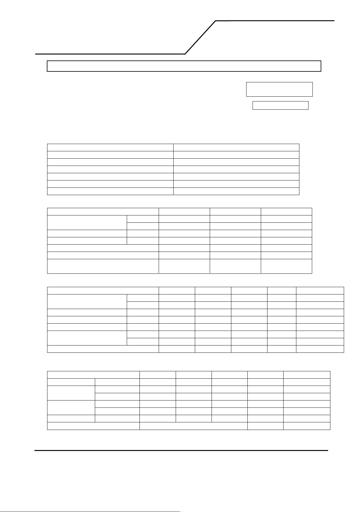
DIMENSIONAL OUTLINE (front)
CN2
LTA084C270F
Unit : mm
Standard tolerance :±0.5
4-7
4-4
(4.5)
MAX12.0
80+/-10
(99.75)
199.5
193.6
191.6
(99.75)
174.8(Bezel Opening)
12.35
191.7+/-0.3
170.4(Active Area)
7.9
3.9
14.55
24.4
12.95
10.75
(76.85)(72.65)
149.5
104.9+/-0.3
127.8(Active Area)
132.2(Bezel Opening)
(2/11) 2007-08-24 (Ver.0.4R)
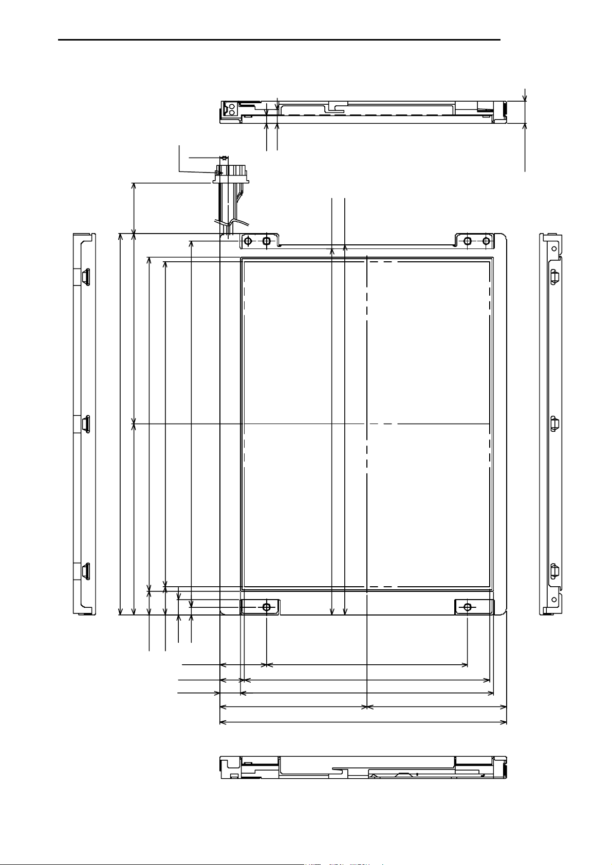
LTA084C270F
DIMENSIONAL OUTLINE (rear)
Unit : mm
Standard tolerance :±0.5
(103.85)
(11)
CN1
Note) The different points between LTA084C270F and LTM08C351L are below.
1) The lamp unit of LTM08C351L can not use for LTA084C270F.
But the lamp unit of LTA084C270F can use for LTM08C351L.
2) The rear structure is changed.
The Metal PCB shield is added and the Plastic frame design is different from LTM08C351L.
There are slight differences. (Refer to page.3 rear dimensional outline in detail.)
3) LTA084C270F Bezel Opening is wider than that of LTM08C351L.
4) The reverse function (REV) is added.
(Refer to page.7 Pin Assignment No.17.)
5) LTA084C270F Viewing angle and Operating temperature are wider than LTM08C351L.
6) LTA084C270F total weight is different from LTM08C351L. (Refer to page.1 mechanical specification.)
(3/11) 2007-08-24 (Ver.0.4R)
BLOCK DIAGRAM
DC/DC
Converter
CN1
Gray Scale
Manipulation
Voltage
Generation
Circuit
*1 Build up LCD drivers on the glass substrate
I/F Connector
Panel
Controller
800 pixels
1, 1 2, 1
1, 2 2,2
X2
X2
n-1
n-1
CCFL Backlight
LCD Panel
800 x 600 pixels
Y-Driver IC
X-Driver IC
, 1 X2n, 1
, 2 X2n, 2
LTA084C270F
Connector
CN2
800, 1
800, 2
1, Y 2, Y
X
, Y X2n, Y
2n-1
1, 600 2, 600
X
, 600 X2n, 600
2n-1
SEQUENCE OF POWER SUPPLIES AND SIGNALS
V
DD
V0.2
10ms (max.)
0.5ms (min.)
3.0
V
40ms (max.)
0ms (min.)
CLK+/RxIN0+/RxIN1+/RxIN2+/-
250ms(min.)
100ms (max.)
0.1ms (min.)
40ms (max.)
0ms (min.)
3sec (min.)
2sec(min.) 0ms(min.)
500ms (min.)
VV3.0
0.2
V
CM
800, Y
800,600
0.2
V
||
ID
V
SFL
600 pixels
V
FL Input Voltage
10%
V
FL
V
SFL
10%
V
FL
(4/11) 2007-08-24 (Ver.0.4R)

r
TIMING CHART
LTA084C270F
ticalTiming
3
t
797 ,Y 799 ,Y
X,598 X,599 X,600
1
2
t
t
3
t
X,Y
X,4
X,3X,2X,1
4
3
t
t
5
t
800 ,Y798 , Y
X,Y
7,Y6,Y5,Y
4,Y
3,Y
2,Y1,Y
NCLK
(1 ) Ve
ENAB
RGB Da ta
(2 ) Hor izon ta l T iming
(5/11) 2007-08-24 (Ver.0.4R)
NCLK
ENAB
RGB Da ta

LTA084C270F
TIMING SPECIFICA TION *
1 *2 *3 *4 *5 *6
Item Symbol Min. Typ. Max. Unit Remarks
Frame Period t1 604 x t3 628 x t3
16.58
Vertical
Display Term
One Line
Scanning Time
Horizontal
Display Term
Clock Period t5 24.7 25.0 27.8 ns
*1 Refer to “TIMING CHART” and LVDS (DC90C365) specifications by National Semiconductor Corporation.
*2 If ENAB is fixed to "H" or "L" level for certain period while NCLK is supplied, the panel displays black with some
flicker.
*3 Don't fix NCLK to "H" or "L" level while the VDD is supplied.
If NCLK is fixed to "H" or "L" level for certain period while ENAB is spplied, the panel may be damaged.
When It holds on, DC voltage supplies to liquid crystal materials and It may cause damage to liquid crystal materials.
*4 Please adjust LCD operating signal timing and FL driving frequency, to optimize the display quality.
There is a possibility that flicker is observed by the interference of LCD operating signal timing and FL driving
condition (especially driving frequency), even if the condition satisfies abov e timing specifications and recommended
operating conditions shown on page 1.
*5 Do not make t1, t2 and t3 fluctuate.
If t1, t2 and t3 are fluctuate, the panel displays black.
*6 Keep constant the number of clock within one line scanning time a nd the number of scanning line within one flame
period.
t2 600 x t3
t3 944 x t5
26.3
t4 800 x t5 800 x t5 800 x t5 ---
600 x t3
1056 x t5
26.4
677 x t3
17.86
600 x t3
1064 x t5
---
---
ms
---
--μs
(6/11) 2007-08-24 (Ver.0.4R)

CONNECTOR PIN ASSIGNMENT FOR INTERFACE
CN1 INPUT SIGNAL
Connector : 20268-020E-12F / I-PEX CO., LTD.
Mating Connector : 20230-020B-F or 20230-T20-F or 20230-W20B-F / I-PEX CO.,LTD.
DF19G-20S-1C(Plug), DF19-2830SCFA(Crimp contact) / HIROSE ELECTRIC CO., LTD.
Terminal No. Symbol Function
1 VDD +3.3V POWER SUPPLY
2 VDD +3.3V POWER SUPPLY
3 GND*1
4 GND*1
5 RxIN0- Negative LVDS differential data input (R0-R5, G0)*3
6 RxIN0+ Positive LVDS differential data input (R0-R5, G0) *3
7 GND*1
8 RxIN1- Negative LVDS differential data input (G1-G5, B0-B1) *3
9 RxIN1+ Positive LVDS differential data input (G1-G5, B0-B1) *3
10 GND*1
11 RxIN2- Negative LVDS differential data input (B2-B5, HS, VS, DE) *3
12 RxIN2+ Positive LVDS differential data input (B2-B5, HS, VS, DE) *3
13 GND*1
14 CLK- Clock Signal (-)
15 CLK+ Clock Signal (+)
16 GND*1
17 REV Display Reverse(“L” level or Open;Normal, “H” l evel; Reverse)
18 GND*1
19 NC*2 Non Connection (open)
20 GND*1
*1 Please connect GND pin to ground. Don’t use it as no-connect nor connection with high impedance.
*2 Please connect NC pin to nothing. Don’t connect it to ground nor to other signal input.
*3 Refer to next page.
CN2 CCFL POWER SOURCE
Connector : BHR-04VS-1/JAPAN SOLDERLESS TERMINAL MFG CO., LTD.
Mating Connector *
Terminal No. Symbol Function
1 VFLH CCFL POWER SUPPLY (HIGH VOLTAGE)
2 VFLH CCFL POWER SUPPLY (HIGH VOLTAGE)
3 NC *2
4 VFLL CCFL POWER SUPPLY (LOW VOLTAGE)
*4 Take away terminal No.3 of the mating connector. If does not take away, it may cause smoke burn of
Electrical parts by high voltage.
4
: SM04(4.0)B-BHS-1-TB/JAPAN SOLDERLESS TERMINAL MFG CO., LTD.
LTA084C270F
(7/11) 2007-08-24 (Ver.0.4R)

LTA084C270F
RECOMMENDED TRANSMITTER (DS90C365)TO LTA084C270F INTERFACE ASSIGNMENT
Case1: 6bit Transmitter
DS90C365
Input Terminal No.
(Graphics controller output signal)
Symbol Terminal Symbol Function
Input Signal
Output Signal
Symbol
TxIN0 44 R0 Red Pixels Display Data (LSB)
TxIN1 45 R1 Red Pixels Display Data
TxIN2 47 R2 Red Pixels Display Data
TxIN3 48 R3 Red Pixels Display Data
TxIN4 1 R4 Red Pixels Display Data
TxOUT0TxOUT0+
TxIN5 3 R5 Red Pixels Display Data (MSB)
TxIN6 4 G0 Green Pixels Display Data (LSB)
TxIN7 6 G1 Green Pixels Display Data
TxIN8 7 G2 Green Pixels Display Data
TxIN9 9 G3 Green Pixels Display Data
TxIN10 10 G4 Green Pixels Display Data
TxIN11 12 G5 Green Pixels Display Data (MSB)
TxOUT1TxOUT1+
TxIN12 13 B0 Blue Pixels Display Data (LSB)
TxIN13 15 B1 Blue Pixels Display Data
TxIN14 16 B2 Blue Pixels Display Data
TxIN15 18 B3 Blue Pixels Display Data
TxIN16 19 B4 Blue Pixels Display Data
TxIN17 20 B5 Blue Pixels Display Data (MSB)
TxIN18 22 NC*1 Non Connection (open)
TxOUT2TxOUT2+
TxIN19 23 NC*1 Non Connection (open)
TxIN20 25 DE Compound Synchronization Signal
TxCLK IN 26 NCLK Data Sampling Clock TxCLK OUT-
TxCLK OUT+
LTA084C270F
Interface
(CN1)
Terminal Symbol
No.5
No.6
No.8
No.9
No.11
No.12
No.14
No.15
RxIN0RxIN0+
RxIN1RxIN1+
RxIN2RxIN2+
CLKCLK+
IN0+ / -
IN1+ / -
IN2+ / -
Tx IN6 Tx IN5 Tx IN4 Tx IN3 Tx IN2 T x IN1 Tx IN0
G0
TxIN13 Tx IN12 Tx IN11 TxIN10 Tx IN9 Tx IN8
B1
Tx IN20
DE
R5
B0
TxIN19 TxIN18 Tx IN17 TxIN16 Tx IN15
NC
R4
G5
NC
R3 R2 R1 R0
G4
B5
G3
B4
G2
Tx IN7
G1
Tx IN14
B2B3
(8/11) 2007-08-24 (Ver.0.4R)

LTA084C270F
RECOMMENDED TRANSMITTER (DS90C385)TO LTA084C270F INTERFACE ASSIGNMENT
Case2: 8bit Transmitter
DS90C385
Input Terminal No.
(Graphics controller output signal)
Symbol Terminal Symbol Function
Input Signal
Output Signal
Symbol
TxIN0 51 R0 Red Pixels Display Data (LSB)
TxIN1 52 R1 Red Pixels Display Data
TxIN2 54 R2 Red Pixels Display Data
TxIN3 55 R3 Red Pixels Display Data
TxIN4 56 R4 Red Pixels Display Data
TxOUT0TxOUT0+
TxIN6 3 R5 Red Pixels Display Data (MSB)
TxIN7 4 G0 Green Pixels Display Data(LSB)
TxIN8 6 G1 Green Pixels Display Data
TxIN9 7 G2 Green Pixels Display Data
TxIN12 11 G3 Green Pixels Display Data
TxIN13 12 G4 Green Pixels Display Data
TxIN14 14 G5 Green Pixels Display Data(MSB)
TxOUT1TxOUT1+
TxIN15 15 B0 Blue Pixels Display Data (LSB)
TxIN18 19 B1 Blue Pixels Display Data
TxIN19 20 B2 Blue Pixels Display Data
TxIN20 22 B3 Blue Pixels Display Data
TxIN21 23 B4 Blue Pixels Display Data
TxIN22 24 B5 Blue Pixels Display Data (MSB)
TxIN24 27 NC*1 Non Connection (open)
TxOUT2TxOUT2+
TxIN25 28 NC*1 Non Connection (open)
TxIN26 30 DE Compound Synchronization Signal
TxIN27 50 NC*1 Non Connection (open)
TxIN5 2 NC*1 Non Connection (open)
TxIN10 8 NC*1 Non Connection (open)
TxIN11 10 NC*1 Non Connection (open)
TxIN16 16 NC*1 Non Connection (open)
TxOUT3TxOUT3+
TxIN17 18 NC*1 Non Connection (open)
TXIN23 25 NC*1 Non Connection (open)
TxCLK IN 31 NCLK Data Sampling Clock TxCLK OUT-
TxCLK OUT+
*1 Please connect NC pin to nothing. Don't connect it to ground nor to other signal input.
LTA084C270F
Interface
(CN1)
Terminal Symbol
No.5
No.6
No.8
No.9
No.11
No.12
No.14
No.15
RxIN0RxIN0+
RxIN1RxIN1+
RxIN2RxIN2+
CLKCLK+
IN0+ / -
IN1+ / -
IN2+ / -
IN3+ / -
Tx IN7 Tx IN6 Tx IN4 Tx IN3 Tx IN2 Tx IN1 Tx IN0
G0
Tx IN18 Tx IN15 Tx IN14 Tx IN13 Tx IN12 Tx IN9
B1
Tx IN26
DE
Tx IN23 Tx IN17 Tx IN16 Tx IN11 Tx IN10 Tx IN5 Tx IN27
NC
R5
B0
Tx IN25 Tx IN24 Tx IN22 Tx IN21 Tx IN20
NC
NC
R4
G5
NC
NC
R3 R2 R1 R0
G4
NC
B5
G3
B4
NC
G2
NC
Tx IN8
G1
Tx IN19
B2B3
NC
(9/11) 2007-08-24 (Ver.0.4R)

LTA084C270F
256k (k=1024) COLORS COMBINATION TABLE
Display R5 R 4 R 3 R2 R 1 R 0 G5 G4 G3 G2 G1 G0 B5 B4 B3 B2 B1 B0 Gray Scale Level
Black L L L L L L L L L L L L L L L L L L ---
Blue L L L L L L L L L L L L H H H H H H ---
Green L L L L L L H H H H H H L L L L L L --Basic
Color
Gray
Scale of
Red
Gray
Scale of
Green
Gray
Scale of
Blue
Gray
Scale of
White &
Black
Light Blue L L L L L L H H H H H H H H H H H H ---
Red H H H H H H L L L L L L L L L L L L --Purple H H H H H H L L L L L L H H H H H H --Yellow H H H H H H H H H H H H L L L L L L ---
White H H H H H H H H H H H H H H H H H H --Black L L L L L L L L L L L L L L L L L L L 0
L L L L L H L L L L L L L L L L L L L 1
Dark
↑
↓
Light
Red H H H H H H L L L L L L L L L L L L Red L63
Black L L L L L L L L L L L L L L L L L L L 0
Dark
↑
↓
Light
Green L L L L L L H H H H H H L L L L L L Green L63
Black L L L L L L L L L L L L L L L L L L L 0
Dark
↑
↓
Light
Blue L L L L L L L L L L L L H H H H H H Blue L63
Black L L L L L L L L L L L L L L L L L L L 0
Dark
↑
↓
Light
White H H H H H H H H H H H H H H H H H H White L63
L L L L H L L L L L L L L L L L L L L 2
:
:
H H H H L H L L L L L L L L L L L L L61
H H H H H L L L L L L L L L L L L L L62
L L L L L L L L L L L H L L L L L L L 1
L L L L L L L L L L H L L L L L L L L 2
:
:
L L L L L L H H H H L H L L L L L L L61
L L L L L L H H H H H L L L L L L L L62
L L L L L L L L L L L L L L L L L H L 1
L L L L L L L L L L L L L L L L H L L 2
:
:
L L L L L L L L L L L L H H H H L H L61
L L L L L L L L L L L L H H H H H L L62
L L L L L H L L L L L H L L L L L H L 1
L L L L H L L L L L H L L L L L H L L 2
:
:
H H H H L H H H H H L H H H H H L H L61
H H H H H L H H H H H L H H H H H L L62
:
:
:
:
:
:
:
:
:
:
:
:
:
:
:
:
L3…
L60
L3…
L60
L3…
L60
L3…
L60
(10/11) 2007-08-24 (Ver.0.4R)

LTA084C270F
!
FOR SAFETY
LCD module is generally designed with precise part s to achieve light weighted thin mechanical dimensions.
In using our Modules, make certain that you fully understand and put into practice the warnings and safety precautions
detailed in Engineering Information No.EE-N001,"CAUTIONS AND INSTRUCTIONS FOR TOSHIBA LCD MODULES".
Refer to individual specifications and TECHNICAL DATA sheets (hereinafter called "TD") for more detailed technical
information.
1) SPECIAL PURPOSES
A) Toshiba Matsushita Display Technology's Standard LCD Modules have not been customized for operation in extreme
environments or for use in applications where performance failures could be life-threatening or otherwise catastrophic.
B) Since Toshiba Matsushita Display Technology's Standard LCD Modules have not been designed for operation in extreme
environments, they must never be used in devices that will be exposed to abnormally high levels of vibration or shock which
exceed Toshiba Matsushita Display Technology's published specification limits.
C) In addition, since Toshiba Matsushita Display Technology Standard LCD Modules have not been designed for use in
applications where performance failures could be life-threatening or catastrophic, they must never be installed in aircraft
navigation control systems (such as, but not limited to Traffic Collision Avoidance System and Air Traffic Indicator), in military
defense or weapons systems, in critical industrial process-control systems (e.g., those involved in the production of nuclear
energy), or in critical medical device or patient life-support systems.
2) DISASSEMBLING OR MODIFICATION
DO NOT DISASSEMBLE OR MODIFY the module. It may damage sensitive parts inside LCD module, and may cause
scratches or dust on the display.
Toshiba Matsushita Display Technology doses not warrant the module, if customer disassembled or modified it.
3) BREAKAGE OF LCD PANEL
DO NOT INGEST liquid crystal material, DO NOT INHALE this material, and DO NOT CONTACT the material with skin, if
LCD panel is broken and liquid crystal material spills out.
If liquid crystal material comes into mouth or eyes, rinse mouth or eyes out with water immediately.
If this material contact with skin or cloths, wash it off immediately with alcohol and rinse thoroughly with water.
4) GLASS OF LCD PANEL
BE CAREFUL WITH CHIPS OF GLASS that may cause injuring fingers or skin, when the glass is broken.
5) ELECTRIC SHOCK
DISCONNECT POWER SUPPLY before handling LCD module.
DO NOT TOUCH the parts inside LCD module and the fluorescent lamp's connector or cables in order to prevent electric
shock, because high voltage is supplied to these parts from the inverter unit while power supply is turned on.
6) ABSOLUTE MAXIMUM RATINGS AND POWER PROTECTION CIRCUIT
DO NOT EXCEED the absolute maximum rating values under the worst probable conditions caused by the supply voltage
variation, input voltage variation, variation in parts' constants, environmental temperature, etc., otherwise LCD module may
be damaged.
Employ protection circuit for power supply, whenever the specification or TD specifies it.
Suitable protection circuit should be applied for each system design.
7) RECOMMENDED OPERATION CONDITIONS
The performance and quality of the LCD panel are warranted only when the LCD panel is used within “the recommended
operation conditions”. Toshiba Matsushita Display Technology Co., Ltd. never warrants the performance and quality of the
LCD panel when you use the LCD panel over “the recommended operation conditions”, although within “the absolute
maximum rating”.
To use the LCD panel over “the recommended operation conditions” may have bad influence on the characteristics and
reliability of the LCD panel and may shorten the life of the LCD panel.
Therefore, when designing the whole set, not to be over “the recommended operation conditions”, you should fully take care
of supply voltage change, characteristic of connection parts, serge of input-and-output line, and surround ing temperature.
8) DISPOSAL
When dispose LCD module, obey to the applicable environmental regulations.
(11/11) 2007-08-24 (Ver.0.4R)
 Loading...