TOSHIBA HD-EP10 Service Manual
SERVICE MANUAL
HD DVD PLAYER
HD-EP10
FILE NO. 810-200751GR
The above models are classified as green products (*1), as indicated by the underlined serial numbers.
This Service Manual describes replacement parts for the green products. When repairing these green
product(s), use the part(s) described in this manual and lead-free solder (*2).
For (*1) and (*2), see the next page.
Apr., 2007 GREEN

(*1) GREEN PRODUCT PROCUREMENT
The EC is actively promoting the WEEE & RoHS Directives that define standards for recycling
and reuse of Waste Electrical and Electronic Equipment and for the Restriction of the use of
certain Hazardous Substances. From July 1, 2006, the RoHS Directive will prohibit any marketing of new products containing the restricted substances.
Increasing attention is given to issues related to the global environmental. Toshiba Corporation
recognizes environmental protection as a key management tasks, and is doing its utmost to
enhance and improve the quality and scope of its environmental activities. In line with this,
Toshiba proactively promotes Green Procurement, and seeks to purchase and use products,
parts and materials that have low environmental impacts.
Green procurement of parts is not only confined to manufacture. The same green parts used in
manufacture must also be used as replacement parts.
(*2) LEAD-FREE SOLDER
This product is manufactured using lead-free solder as a part of a movement within the consumer products industry at large to be environmentally responsible. Lead-free solder must be
used in the servicing and repair of this product.
WARNING
This product is manufactured using lead free solder.
DO NOT USE LEAD BASED SOLDER TO REPAIR THIS PRODUCT !
The melting temperature of lead-free solder is higher than that of leaded solder by 86°F to
104°F (30°C to 40°C). Use of a soldering iron designed for lead-based solders to repair product
made with lead-free solder may result in damage to the component and or PCB being soldered.
Great care should be made to ensure high-quality soldering when servicing this product especially when soldering large components, through-hole pins, and on PCBs as the level of heat
required to melt lead-free solder is high.

SAFETY INSTRUCTIONS
WARNING: BEFORE SERVICING THIS CHASSIS, READ THE 웃SAFETY PRECAUTION웃
AND 웃PRODUCT SAFETY NOTICE웃INSTRUCTIONS BELOW.
SAFETY PRECAUTION
WARNING: SERVICE SHOULD NOT BE ATTEMPTED BY ANYONE UNFAMILIAR WITH THE NECESSARY
PRECAUTIONS ON THIS RECEIVER. THE FOLLOWING ARE THE NECESSARY PRECAUTIONS TO BE
OBSERVED BEFORE SERVICING THIS CHASSIS.
ሩAn isolation transformer should be connected in the power line between the product and the AC line before any service
is performed on the product.
ሩWhen replacing a chassis in the cabinet, always be certain that all the protective devices are put back in place, such as;
nonmetallic control knobs, insulating covers, shields, isolation resistor-capacitor network etc.
ሩAlways advise users to keep children away. There is danger of injury to children from tools, disassembled products, etc.
ሩAlways disconnect the power plug before starting work whenever power is not required. Failure to disconnect the power
plug before starting work can result in electrical shock.
ሩDepending on the model, use an insulation transformer or wear gloves when servicing with the power on, and disconnect
the power plug to avoid electrical shock when replacing parts. In some cases, alternating current is also impressed in
the chassis, so electrical shock is possible if the chassis is contacted with the power on.
ሩAlways use the replacement parts specified for the particular model when making repairs. The parts used in products
have the necessary safety characteristics such as inflammability, voltage resistance, etc. ; therefore, use only
replacement parts that have these same characteristics. Use only the specified parts when the mark is
include in a circuit diagram or parts list.
ሩParts mounting and routing of the wiring should be the same as that used originally. For safety purposes, insulating materials
such as tubing or tape is sometimes used and printed circuit boards are sometimes mounted floating. Also make sure that
wiring is routed and clamped to avoid parts that generate heat and which use high voltage. Always follow the original scheme.
ሩAfter a repair has been completed, reassemble all disassembled pars, and route and reconnect the wiring, in accordance with
the original scheme. Do not allow internal wiring to be pinched by cabinets, panels, etc. Any error in reassembly or wiring
can result in electrical leakage, flame, etc.,and may be hazardous.
ሩNever remodel the product in any way. Remodeling can result in improper operation, malfunction, or electrical leakage and
flame, which may be hazardous.
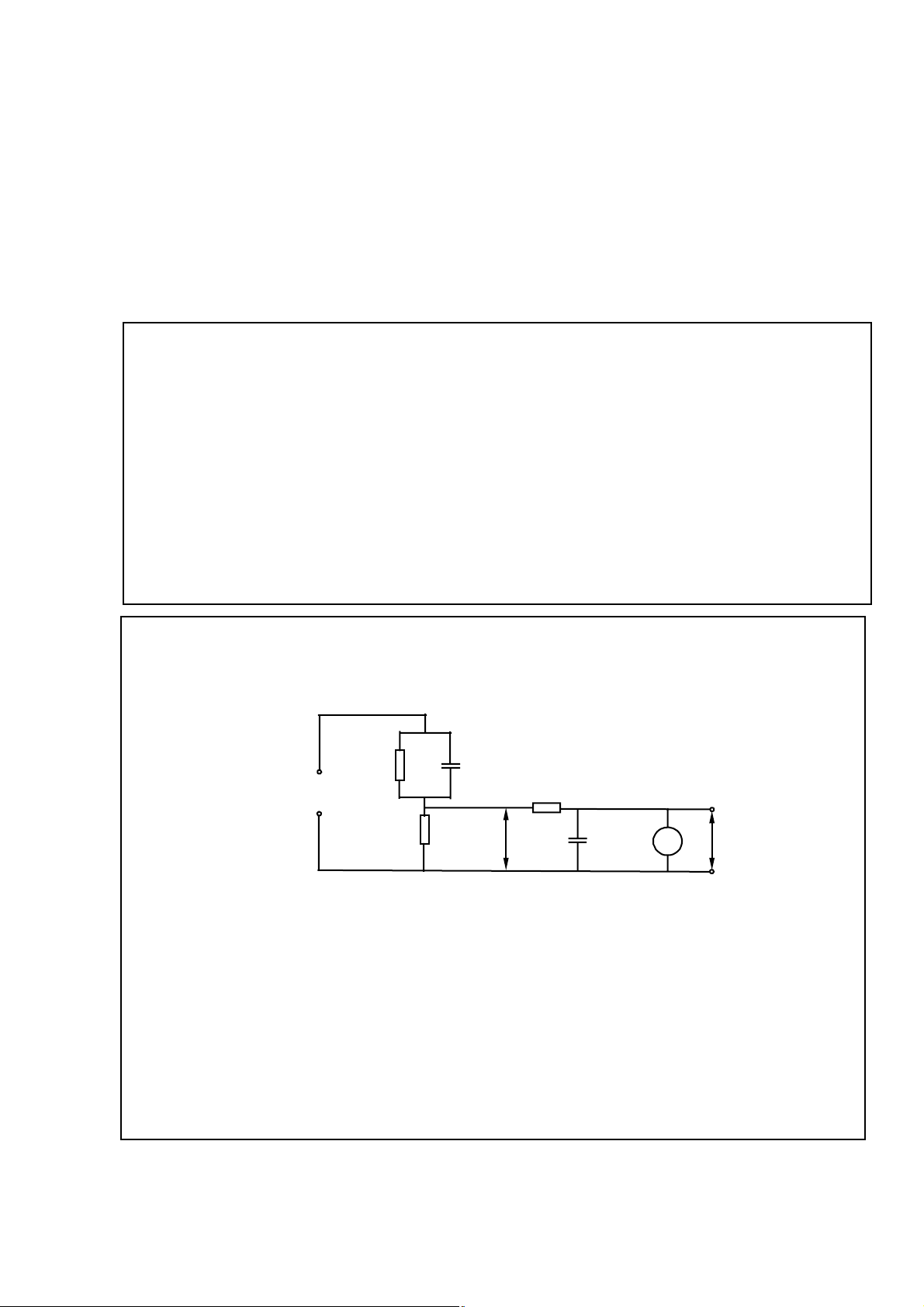
Touch current check
(After completing the work, measure touch current to prevent an electric shock.)
ሩPlug the AC cord directly into the AC outlet. Do not use an isolation transformer for this check..
ሩConnect a measuring network for touch currents between each exposed metallic part on the set and a good earth
ground such as a water pipe, as shown in Figure D.1
ሩThe potential at any point(TOUCH CURRENT) expressed as voltage U
The part or contact of a TERMINAL is not HAZARDOUS LIVE if:
a) the open-circuit voltage does not exceed 35 V (peak) a.c or 60 V d.c.,
or,if a)is not met,
b) the measurement of the TOUCH-CURRENT shall be carried out in accordance with IEC 60990, with the measuring network
described in annex D of this standard.
The TOUCH CURRENT expressed as voltages U
- for a.c.:U
- for d.c.:U
NOTE 5 -The limit values of U
mA 2,0mA d.c.
The limit value U
1
= 35 V(peak)and U2=0.35 V (perk);
1
= 1,0 V,
2
=0.35 V (peak) for a.c. and U1=1.0 V for d.c. correspond, to the values 0,7mA (peak) a.c. and 2,0
1
= 35 V (peak) for a.c. corresponds to the value 70mA (peak) a.c. for frequencies greater than 100 kHz.
1
and U2 does not exceed the following value:
1
and U2, does not exceed the following values:
Measuring network for TOUCH CURRENTS
Annex D
(normative)
Test TERMINALS
A
B
Rs=
1 500ǡ
R
b
500ǡ
=
Cs=
0.22uF
10kǡ
U
1
0.022uF
V
(V)
U
2
Resistance values in ohms(˖)
V: Voltmeter or oscilloscope
(r.m.s or peak reading)
Input resistance: 싫1 M˖
Input capacitance: 싪 200 pF
Frequency range: 15 Hz to 1 MHz and d.c. respectively
NOTE-Appropriate measures should be taken to obtain the correct value in case of non-sinusoidal waveforms.
2
The measuring instrument is calibrated by comparing the frequency factor of U
with the solid line in figure F.2 of
IEC 60990 at various frequencies. A calibration curve is constructed showing the deviation of U
curve as a function of frequency.
TOUCH CURRENT=U
2
/500(peak value)
IEC 802/96
2
from the ideal
Fig.D.1
PRODUCT SAFETY NOTICE
The use of substitute replacement parts which do not have the same safety characteristics as specified in the parts list
Many electrical and mechanical parts in this chassis have special safety-related characteristics. These characteristics
are often passed unnoticed by a visual inspection and the protection afforded by them cannot necessarily be obtained by
using replacement components rated for higher voltage, wattage, etc. Replacement parts which have these special
safety characteristics are identified in this manual and its supplements; electrical components having such features are
identified by the international hazard symbols on the schematic diagram and the parts list.
Before replacing any of these components, read the parts list in this manual carefully.
may create shock, fire, or other hazards.
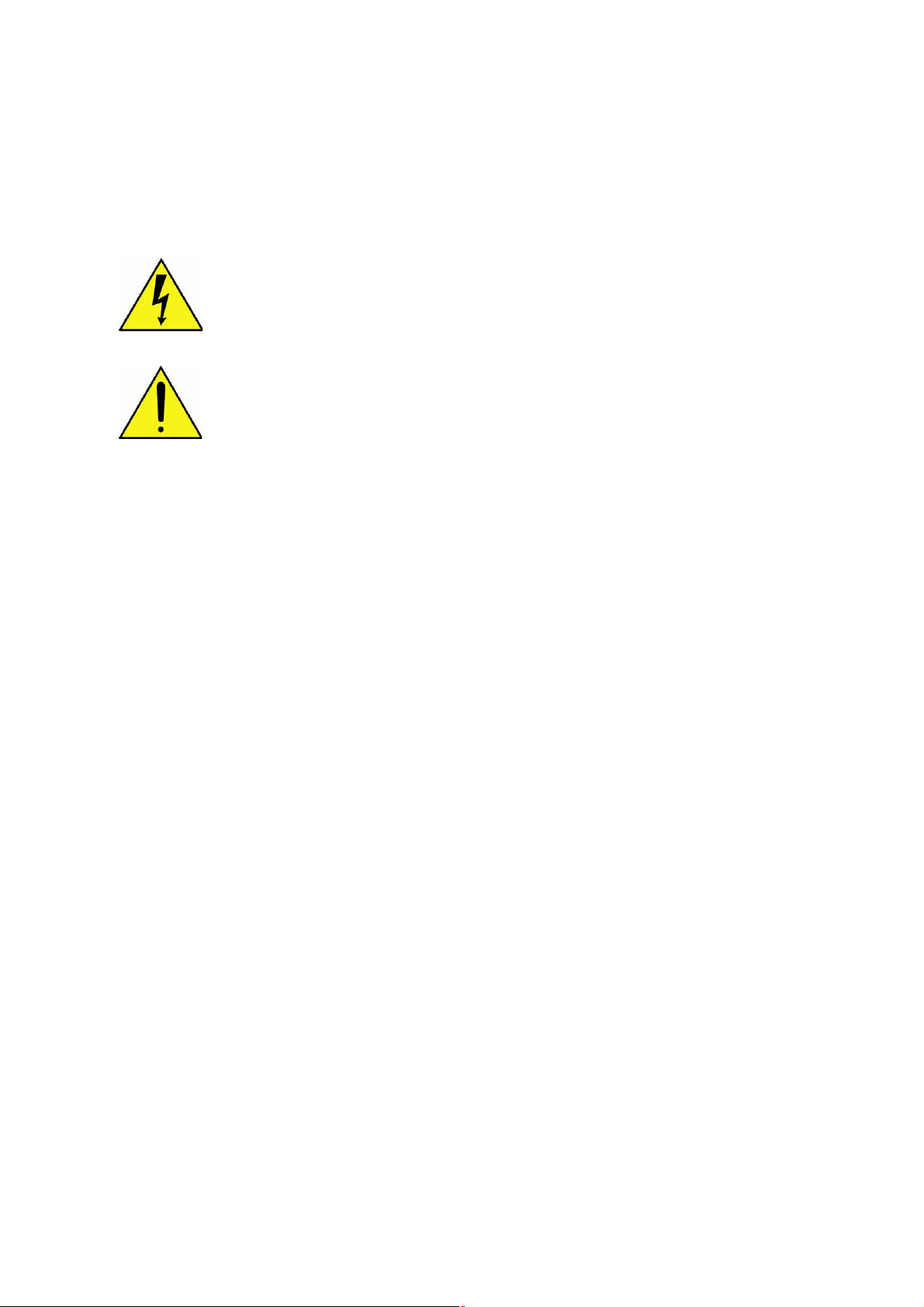
The lightning flash with arrowhead symbol, within an equilateral triangle, is intended to alert the user
to the presence of uninsulated “ dangerous voltage ” within the products enclosure that may be of
sufficient magnitude to constitute a risk of electric shock to persons.
The exclamation point within an equilateral triangle is intended to alert the user to the presence of
important operating and maintenance (servicing) instructions in the literature accompanying the
appliance.
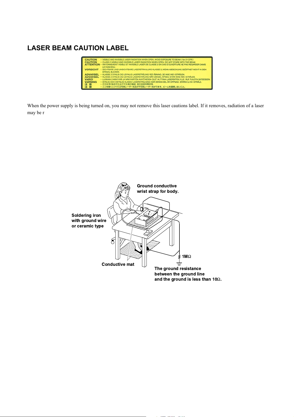
LASER BEAM CAUTION LABEL
When the power supply is being turned on, you may not remove this laser cautions label. If it removes, radiation of a laser
may be received.
PREPARATION OF SERVICING
Pickup Head consists of a laser diode that is very susceptible to external static electricity.
Although it operates properly after replacement, if it was subject to electrostatic discharge during replacement,
its life might be shortened. When replacing, use a conductive mat, soldering iron with ground wire, etc. to
protect the laser diode from damage by static electricity.
And also, the LSI and IC are same as above.
Ground conductive
wrist strap for body.
Soldering iron
with ground wire
or ceramic type
1M
9
Conductive mat
Dolby features manufactured under license from Dolby Laboratories. Dolby and the double-D symbol are trademarks of Dolby Laboratories.
·
Manufactured under license from DTS, Inc. under one or more of the following U.S. Pat. No's. 5,451,942; 5,956,674; 5,974,380; 5,978,762; 6,226,616;
·
6,487,535 and other U.S. and world-wide patents issued and pending. "DTS" and "DTS Digital Surround" are registered trademarks of DTS, Inc.
HDMI, the HDMI logo and High-Definition Multimedia Interface are trademarks or registered trademarks of HDMI Licensing LLC.
·
SHARC is a registered trademark and Melody is a trademark of Analog Devices, Inc.
·
All other brand and product names mentioned in this manual are trademarks and/or registered trademarks of their respective holders.
·
The ground resistance
between the ground line
and the ground is less than 109.

1. OPERATING INSTRUCTIONS
CONTENTS
SECTION 1
GENERAL DESCRIPTIONS
2. LOCATION OF MAIN PARTS
2-1. Location of Main Parts
2-2. Location of PC Boards
1. REPLACEMENT OF MECHANICAL PARTS
1-1. Front Panel, Front PC Boards
1-2. Main/Power PC Boards
1-3. DVD Drive
1. CIRCUIT SYMBOLS AND
SUPPLEMENTARY EXPLANATION
1-1. Precautions for Part Replacement
1-2. Solid Resistor Indication
1-3. Capacitance Indication
1-4. Inductor Indication
1-5. Waveform and Voltage Measurement
1-6. Others
2. PRINTED WIRING BOARD AND
SCHEMATIC DIAGRAM
3. SYSTEM BLOCK DIAGRAM
4. CIRCUIT DIAGRAMS
4-1. Power Supply Circuit Diagram
4-2. Front Circuit Diagram
4-2-1. Front FIP Circuit Diagram
4-2-2. Power Switch Circuit Diagram
4-2-3. Front Switch/USB Circuit Diagram
4-3. ATAPI Conversion Circuit Diagram
PART REPLACEMENT PROCEDURES
SECTION 2
2. WIRING CONNECTION DIAGRAM
2-1. Wiring Connection Diagram
2-2. Supplementary Instructions for Reassembling
SECTION 3
SERVICING DIAGRAMS
4-4. Main Circuit Diagram
4-4-1. AV Output Circuit Diagram
4-4-2. Timer Circuit Diagram
5. PC BOARDS
5-1. Front FIP PC Board
5-2. Power Switch PC Board
5-3. Front Switch/USB PC Board
5-4. ATAPI PC Board
SAFETY PRECAUTION
NOTICE
ABBREVIATIONS
1. EXPLODED VIEWS
1-1. Packing Assembly
1-2. Chassis Assembly
2. PARTS LIST
SECTION 4
PARTS LIST

GENERAL DESCRIPTIONS
SECTION 1
GENERAL DESCRIPTIONS
1. OPERATING INSTRUCTIONS
Please refer to the owner's manual about the contents.
SECTION 1
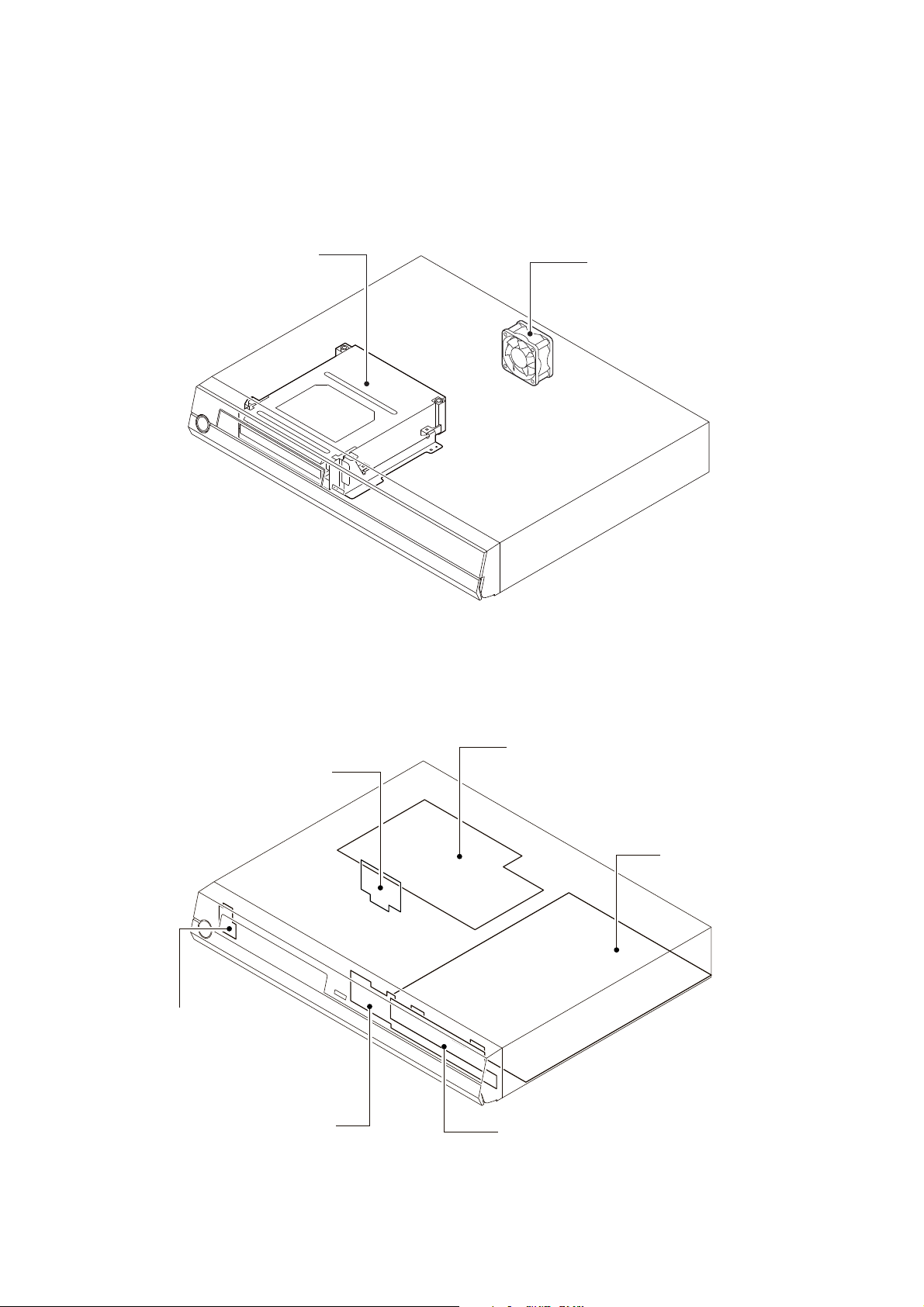
2. LOCATION OF MAIN PARTS
2-1. Location of Main Parts
RAM1 DVD Drive
FAN1 Fan
Fig. 1-2-1
2-2. Location of PC Boards
ATA1 ATAPI PC board
PSW1 Power switch PC board
USB1 Front switch/USB PC board
PWR1 Power PC board
U001 Main PC board
FRT1 Front FIP PC board
Fig. 1-2-2
SECTION 2
PART REPLACEMENT PROCEDURES
CAUTIONS BEFORE STARTING PART REPLACEMENT
Electronic parts are susceptible to static electricity and may easily damaged, so do not forget to ground as required.
Many screws are used inside the unit. To prevent the screws from missing or dropping, etc. always use a magnetized
screwdriver in servicing. Several kinds of screws are used and some of them need special cautions. That is, take care of
the tapping screws securing molded parts and fine pitch screws used to secure metal parts. If they are used improperly,
the screw holes will be easily damaged and the parts can not be fixed.
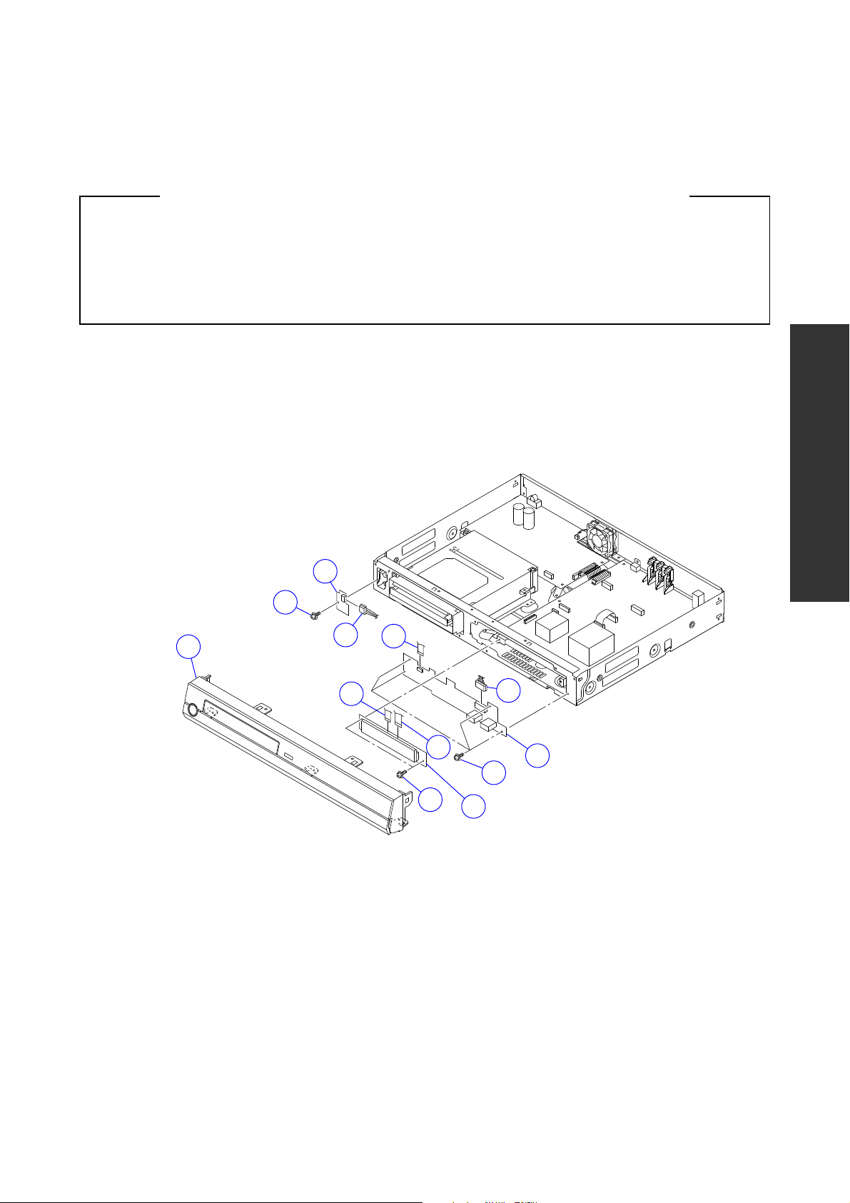
1. REPLACEMENT OF MECHANICAL PARTS
Note:
• Circled numbers in the figure show the main disassembly procedure. Refer to them when disassembling.
1-1. Front Panel, Front PC Boards
PART REPLACEMENT PROCEDURES
SECTION 2
Front panel
Power Switch PC board
3
1
4
2
8
5
5
9
11
Front Switch/USB PC board
10
6
Fig. 2-1-1
7
Front FIP PC board
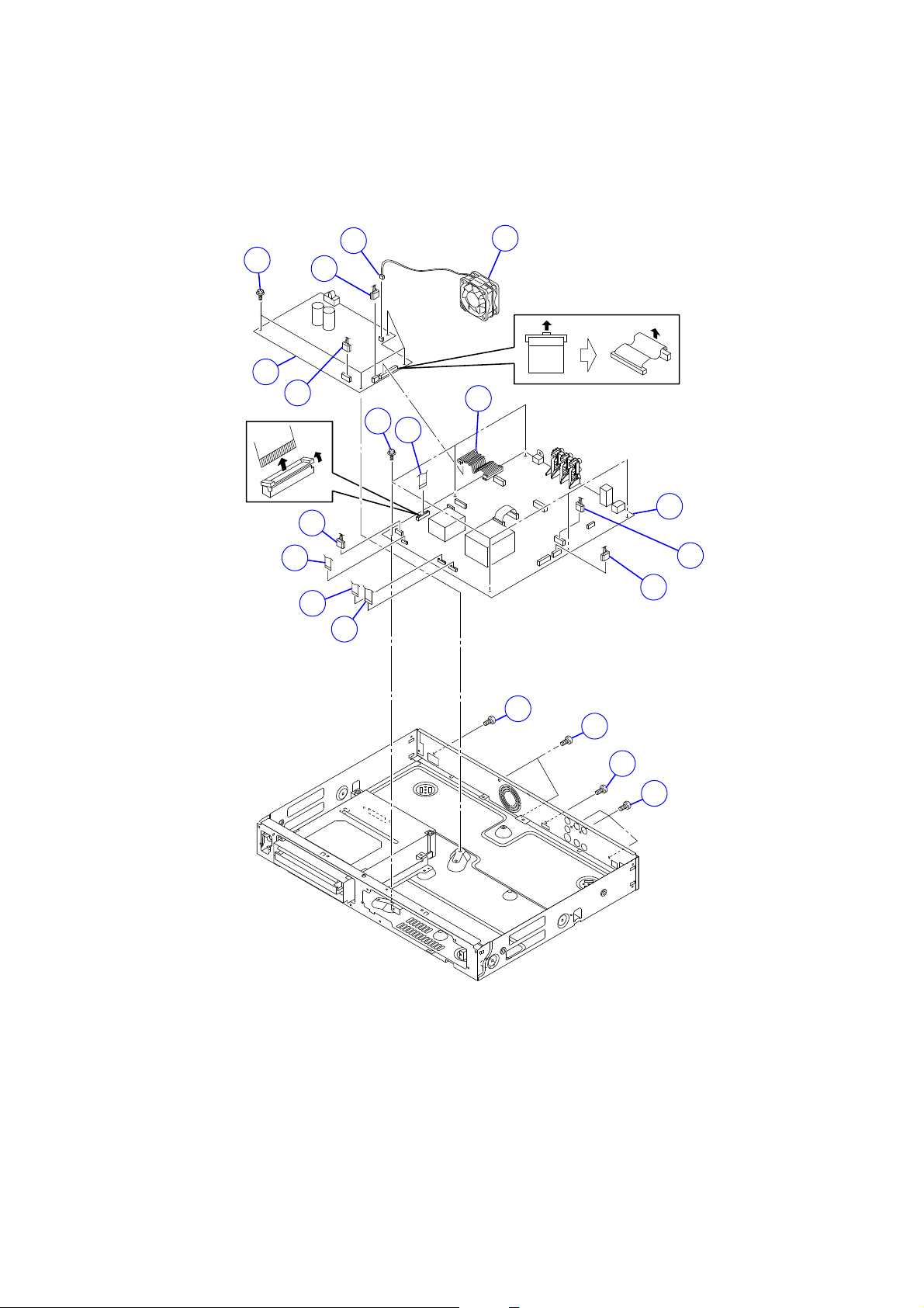
1-2. Main/Power PC Boards
6
Fan
2
3
4
Power PC board
7
4
11
9
5
12
MainPC board
10
9
10
10
9
9
1
1
8
8
Fig. 2-1-2
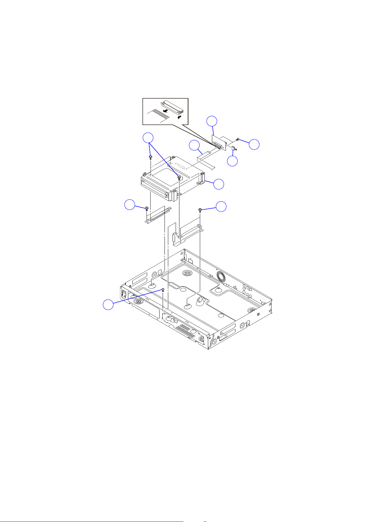
1-3. DVD Drive
ATAPI PC board
5
6
2
4
3
7
DVD Drive
1
1
1
Fig. 2-1-3
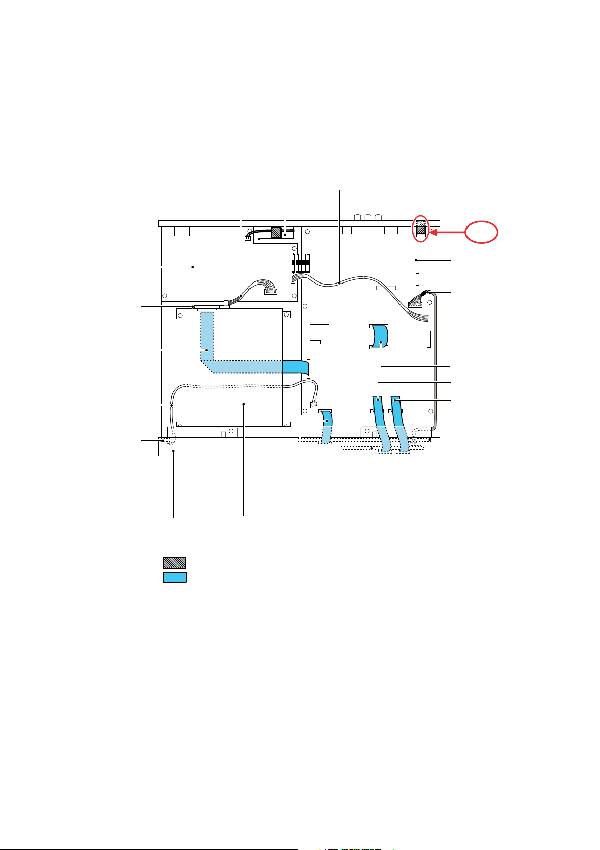
2. WIRING CONNECTION DIAGRAM
2-1. Wiring Connection Diagram
After the servicing is complete, return the wiring to its original state by using the diagram below as a reference.
W104W102
FAN
A-1
Power PC board
ATAPI PC board
W004
W103
Power switch
PC board
Front panel
DVD Drive
W001
Front FIP PC board
Main PC board
W101
W005
W003
W002
Front switch/US
PC board
B
: Tape
: Flexible cable
Fig. 2-2-1
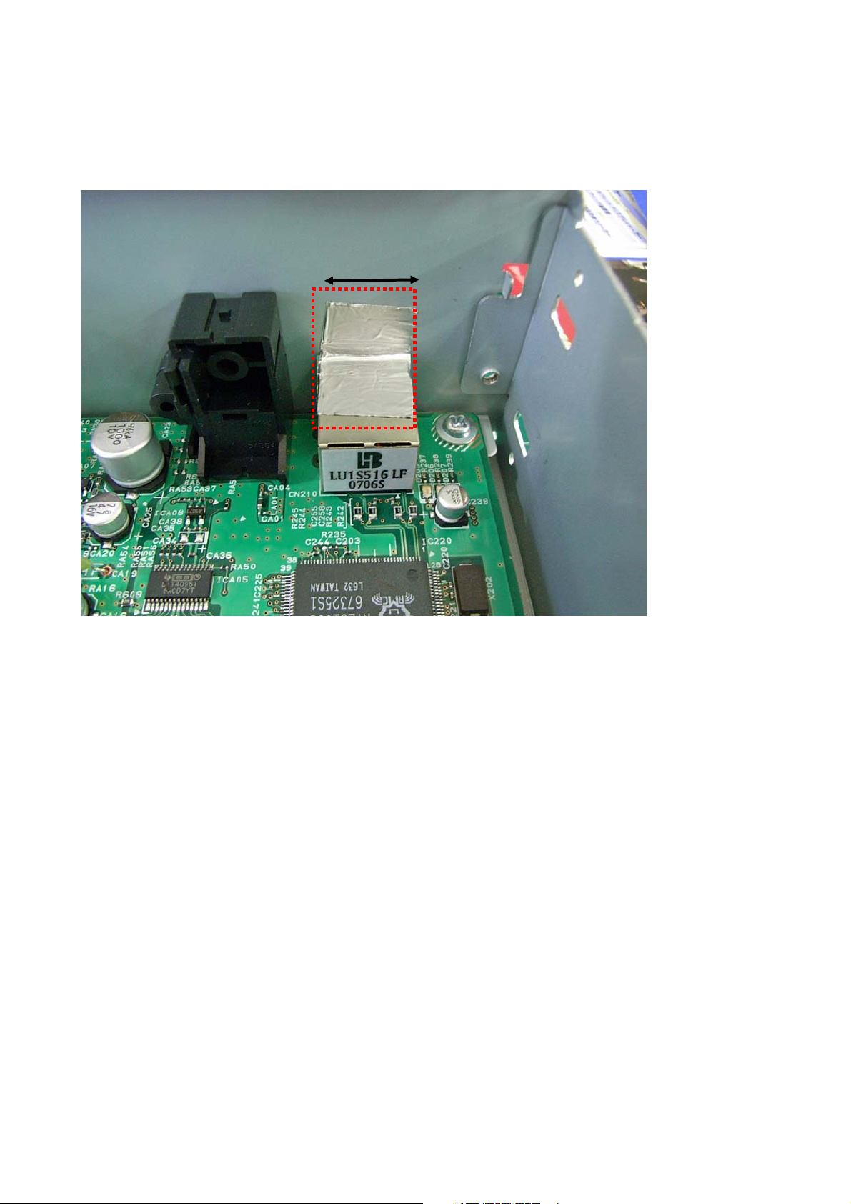
2-2. Supplementary Instructions for Reassembling
A-1. Paste aluminum tape (AL-25T,15mm) between LAN Jack (CN210) and rear panel as follows.
15mm
SECTION 3
SERVICING DIAGRAMS
1. CIRCUIT SYMBOLS AND SUPPLEMENTARY EXPLANATION
1-1. Precautions for Part Replacement
• In the schematic diagram, parts marked (ex.
F801) are critical part to meet the safety regulations, so
always use the parts bearing specified part codes (SN)
when replacing them.
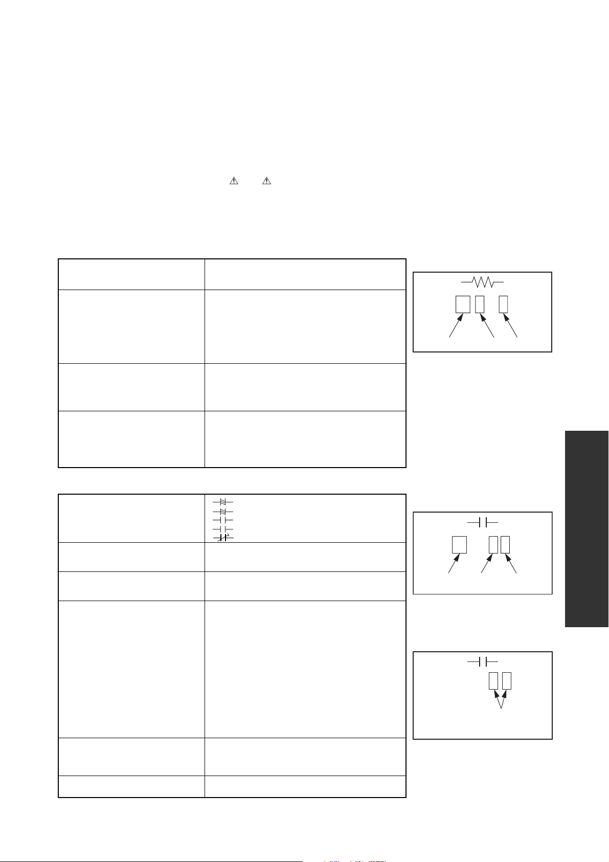
1-2. Solid Resistor Indication
Unit None ........... Ω
K ........... kΩ
M ........... MΩ
Tolerance None ........... ±5%
B ........... ±0.1%
C ........... ±0.25%
D ........... ±0.5%
F ...........±1%
G ........... ±2%
K ........... ±10%
M ........... ±20%
Rated Wattage (1) Chip Parts
None .........1/16W
(2) Other Parts
None .........1/6W
Other than above, described in the Circuit Diagram.
Type None ........... Carbon film
S ...........Solid
R ........... Oxide metal film
M ........... Metal film
W ...........Cement
FR ........... Fusible
• Using the parts other than those specified shall violate
the regulations, and may cause troubles such as
operation failures, fire etc.
Eg. 1
100k
Rated Wattage Type Tolerance
Fig. 3-1-1
SERVICING DIAGRAMS
1-3. Capacitance Indication
Symbol
Unit None ........... F
Rated voltage None ........... 50V
Tolerance (1) Ceramic, plastic, and film capacitors of which
Temperature characteristic None ........... SL
(Ceramic capacitor) For others, temperature characteristics are
Static electricity capacity Sometimes described with abbreviated letters as
(Ceramic capacitor) shown in Eg. 3.
+
........... Electrolytic, Special electrolytic
NP
........... Non polarity electrolytic
........... Ceramic, plastic
M
........... Film
........... Trimmer
μ ...........μF
p ........... pF
For other than 50V and electrolytic capacitors,
described in the Circuit Diagram.
capacitance are more than 10 pF.
None ........... ±5% or more
B ........... ±0.1%
C ........... ±0.25%
D ........... ±0.5%
F ...........±1%
G ........... ±2%
(2) Ceramic, plastic, and film capacitors of which
capacitance are 10 pF or less.
None ........... more than ±5 pF
B ........... ±0.1 pF
C ........... ±0.25 pF
(3) Electrolytic, Trimmer
Tolerance is not described.
described. (For capacitors of 0.01 μF and
no indications are described as F.)
Eg. 2
100μ
Temperature
response
Rated
voltage
Tolerance
Fig. 3-1-2
Eg. 3
104
4
pF (0.1μF)
10x10
Temperature characteristic
(or Temperature characteristic+
Static electricity capacity tolerance)
Fig. 3-1-3
SECTION 3
 Loading...