


SERVICE MANUAL
HD DVD PLAYER
HD-A2KU
FILE NO. 810-200685GR
Rev.01
HD-A2WKU
HD-D2KU
HD-A2KC
(HD-A2KU)
The above models are classified as green products (*1), as indicated by the underlined serial numbers.
This Service Manual describes replacement parts for the green products. When repairing these green
product(s), use the part(s) described in this manual and lead-free solder (*2).
For (*1) and (*2), see the next page.
Dec., 2006 GREEN

(*1) GREEN PRODUCT PROCUREMENT
The EC is actively promoting the WEEE & RoHS Directives that define standards for recycling
and reuse of Waste Electrical and Electronic Equipment and for the Restriction of the use of
certain Hazardous Substances. From July 1, 2006, the RoHS Directive will prohibit any marketing of new products containing the restricted substances.
Increasing attention is given to issues related to the global environmental. Toshiba Corporation
recognizes environmental protection as a key management tasks, and is doing its utmost to
enhance and improve the quality and scope of its environmental activities. In line with this,
Toshiba proactively promotes Green Procurement, and seeks to purchase and use products,
parts and materials that have low environmental impacts.
Green procurement of parts is not only confined to manufacture. The same green parts used in
manufacture must also be used as replacement parts.
(*2) LEAD-FREE SOLDER
This product is manufactured using lead-free solder as a part of a movement within the consumer products industry at large to be environmentally responsible. Lead-free solder must be
used in the servicing and repair of this product.
WARNING
This product is manufactured using lead free solder.
DO NOT USE LEAD BASED SOLDER TO REPAIR THIS PRODUCT !
The melting temperature of lead-free solder is higher than that of leaded solder by 86°F to
104°F (30°C to 40°C). Use of a soldering iron designed for lead-based solders to repair product
made with lead-free solder may result in damage to the component and or PCB being soldered.
Great care should be made to ensure high-quality soldering when servicing this product especially when soldering large components, through-hole pins, and on PCBs as the level of heat
required to melt lead-free solder is high.
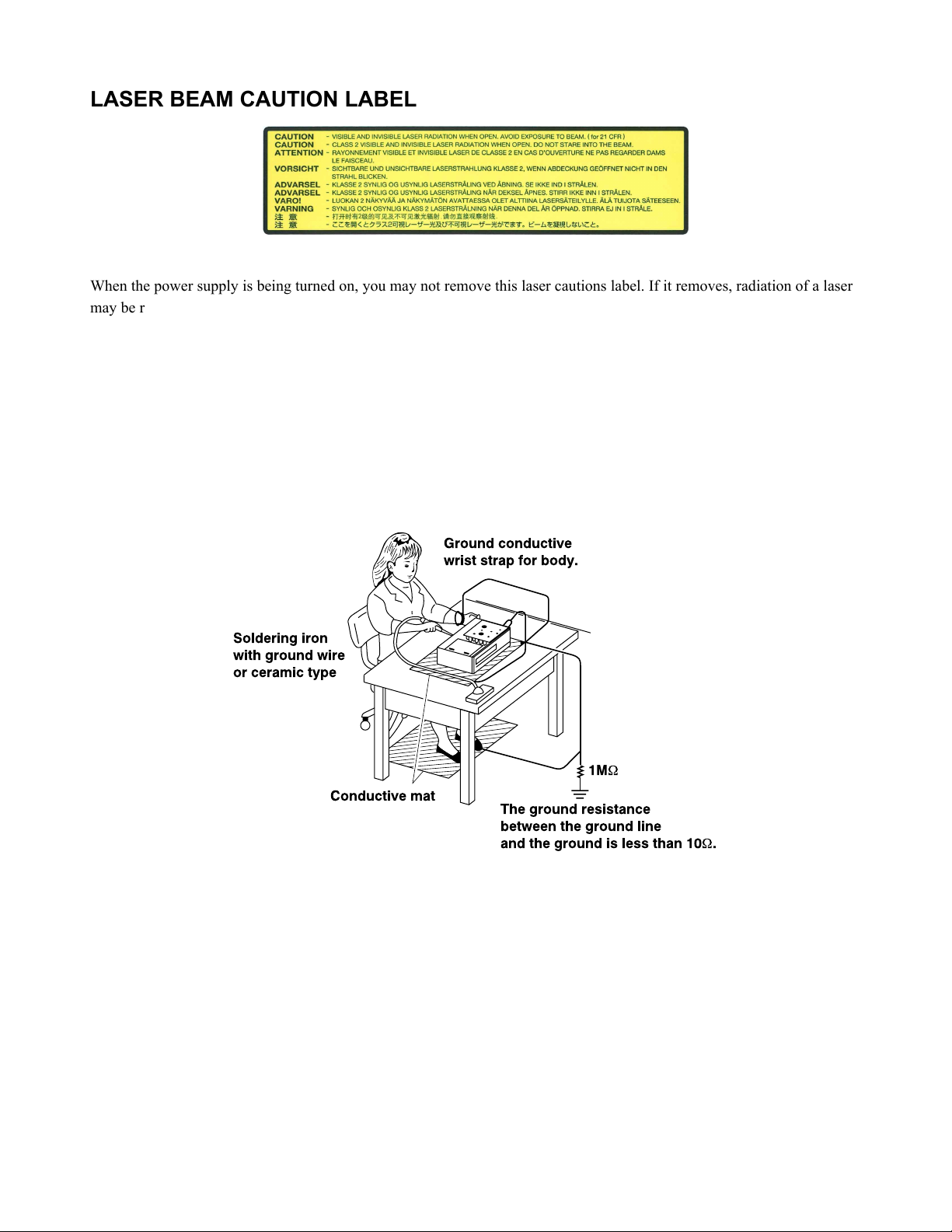
LASER BEAM CAUTION LABEL
When the power supply is being turned on, you may not remove this laser cautions label. If it removes, radiation of a laser
may be received.
PREPARATION OF SERVICING
Pickup Head consists of a laser diode that is very susceptible to external static electricity.
Although it operates properly after replacement, if it was subject to electrostatic discharge during replacement,
its life might be shortened. When replacing, use a conductive mat, soldering iron with ground wire, etc. to
protect the laser diode from damage by static electricity.
And also, the LSI and IC are same as above.
9
Dolby features manufactured under license from Dolby Laboratories. Dolby and the double-D symbol are trademarks of Dolby Laboratories.
·
DTS features manufactured under license from Digital Theater Systems, Inc. U.S. Pat. No's. 5,451,942; 5,956,674; 5,974,380; 5,978,762; 6,226,616;
·
6,487,535 and other U.S. and world-wide patents issued and pending. "DTS" and "DTS Digital Surround" are registered trademarks of Digital Theater
Systems, Inc.
Copyright 1996, 2003 Digital Theater Systems, Inc. All Rights Reserved.
HDMI, the HDMI logo and High-Definition Multimedia Interface are trademarks or registered trademarks of HDMI Licensing LLC.
·
SHARC is a registered trademark and Melody is a trademark of Analog Devices, Inc.
·
All other brand and product names mentioned in this manual are trademarks and/or registered trademarks of their respective holders.
·
9
SAFETY NOTICE
SAFETY PRECAUTIONS
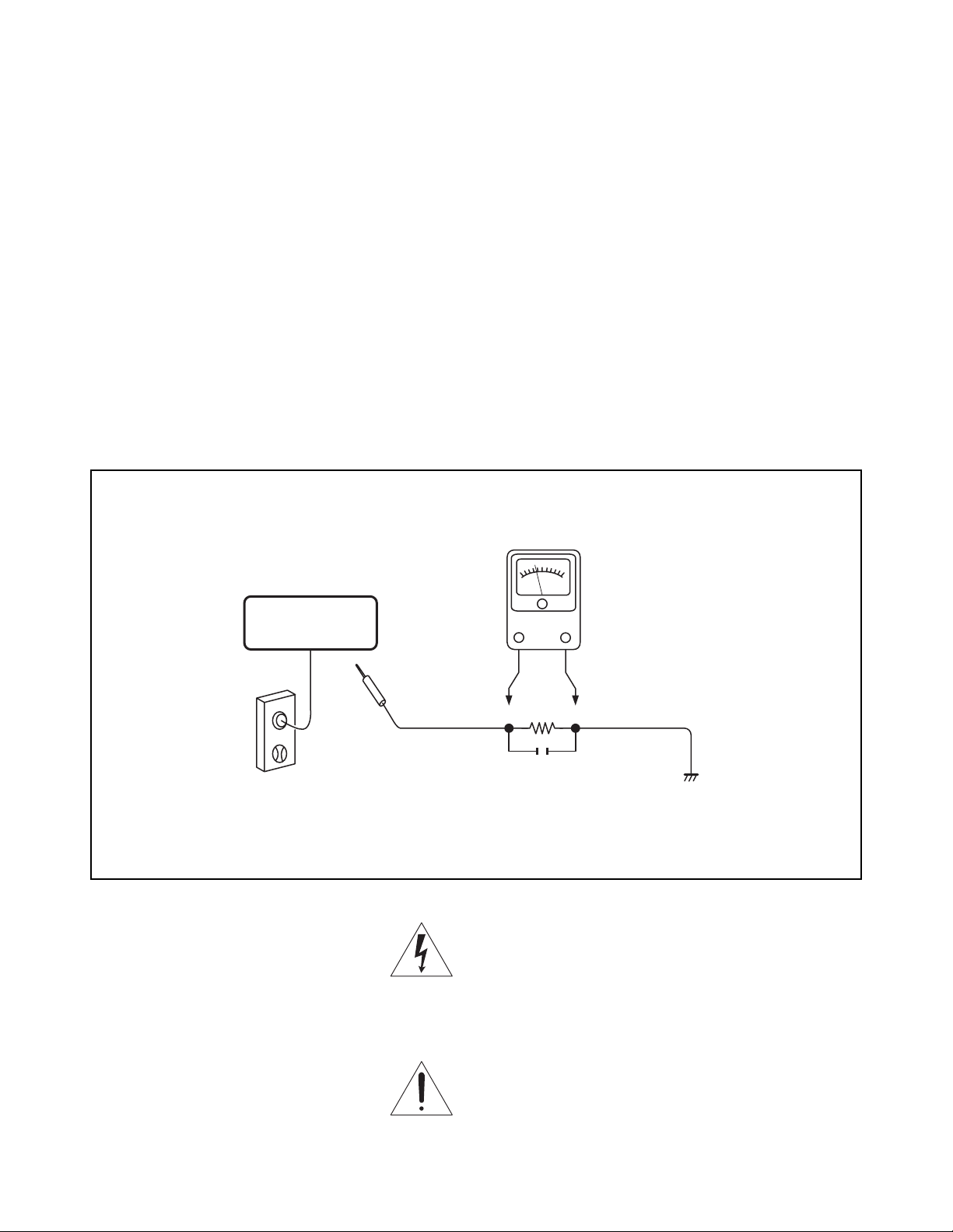
LEAKAGE CURRENT CHECK
Plug the AC line cord directly into a 120V AC outlet (do
not use an isolation transformer for this check). Use an
AC voltmeter, having 5000 Ω per volt or more sensitivity.
Connect a 1500 Ω 10 W resistor, paralleled by a 0.15 µF
150V AC capacitor between a known good earth ground
(water pipe, conduit, etc.) and all exposed metal parts of
cabinet (antennas, handle bracket, metal cabinet
screwheads, metal overlays, control shafts, etc.).
READING SHOULD NOT EXCEED 0.3V
Measure the AC voltage across the 1500 Ω resistor.
The test must be conducted with the AC switch on and
then repeated with the AC switch off. The AC voltage
indicated by the meter may not exceed 0.3 V. A reading
exceeding 0.3 V indicates that a dangerous potential
exists, the fault must be located and corrected.
Repeat the above test with the DVD PLAYER power plug
reversed.
NEVER RETURN A DVD PLAYER TO THE CUS-
TOMER WITHOUT TAKING NECESSARY CORREC-
TIVE ACTION.
DVD PLAYER
AC OUTLET
AC VOLTMETER
(5000 Ω per volt
or more sensitivity)
Good earth ground
such as a water pipe,
1500 Ω
10 W
0.15 µF 150V AC
conduit, etc.
Test all exposed metal.
Voltmeter Hook-up for Leakage Current Check
The lightning flash with arrowhead symbol, within an
equilateral triangle, is intended to alert the user to the
presence of uninsulated “dangerous voltage” within the
product’s enclosure that may be of sufficient magnitude to
constitute a risk of electric shock to persons.
The exclamation point within an equilateral triangle is
intended to alert the user to the presence of important
operating and maintenance (servicing) instructions in the
literature accompanying the appliance.

1. OPERATING INSTRUCTIONS
CONTENTS
SECTION 1
GENERAL DESCRIPTIONS
2. LOCATION OF MAIN PARTS
2-1. Location of Main Parts
2-2. Location of PC Boards
1. REPLACEMENT OF MECHANICAL PARTS
1-1. Front Panel, Front PC Boards
1-2. Main/Power PC Boards
1-3. DVD Drive
1. CIRCUIT SYMBOLS AND
SUPPLEMENTARY EXPLANATION
1-1. Precautions for Part Replacement
1-2. Solid Resistor Indication
1-3. Capacitance Indication
1-4. Inductor Indication
1-5. Waveform and Voltage Measurement
1-6. Others
2. PRINTED WIRING BOARD AND
SCHEMATIC DIAGRAM
3. BLOCK DIAGRAMS
4. CIRCUIT DIAGRAMS
4-1. Power Supply Circuit Diagram
4-1-1. Power Supply Circuit Diagram (Type A)
4-1-2. Power Supply Circuit Diagram (Type B)
4-2. Front Circuit Diagram
4-2-1. Front FIP Circuit Diagram
4-2-2. Power Switch Circuit Diagram
4-2-3. Front Switch/USB Circuit Diagram
4-3. ATAPI Conversion Circuit Diagram
PART REPLACEMENT PROCEDURES
SECTION 2
2. WIRING CONNECTION DIAGRAM
SECTION 3
SERVICING DIAGRAMS
4-4. Main Circuit Diagram
4-4-1. AV Output Circuit Diagram
4-4-2. Timer Circuit Diagram
5. PC BOARDS
5-1. Front FIP PC Board
5-2. Power Switch PC Board
5-3. Front Switch/USB PC Board
5-4. ATAPI PC Board
SAFETY PRECAUTION
NOTICE
ABBREVIATIONS
1. EXPLODED VIEWS
1-1. Packing Assembly
1-2. Chassis Assembly
SECTION 4
PARTS LIST

GENERAL DESCRIPTIONS
SECTION 1
GENERAL DESCRIPTIONS
1. OPERATING INSTRUCTIONS
Please refer to the owner's manual about the contents.
SECTION 1
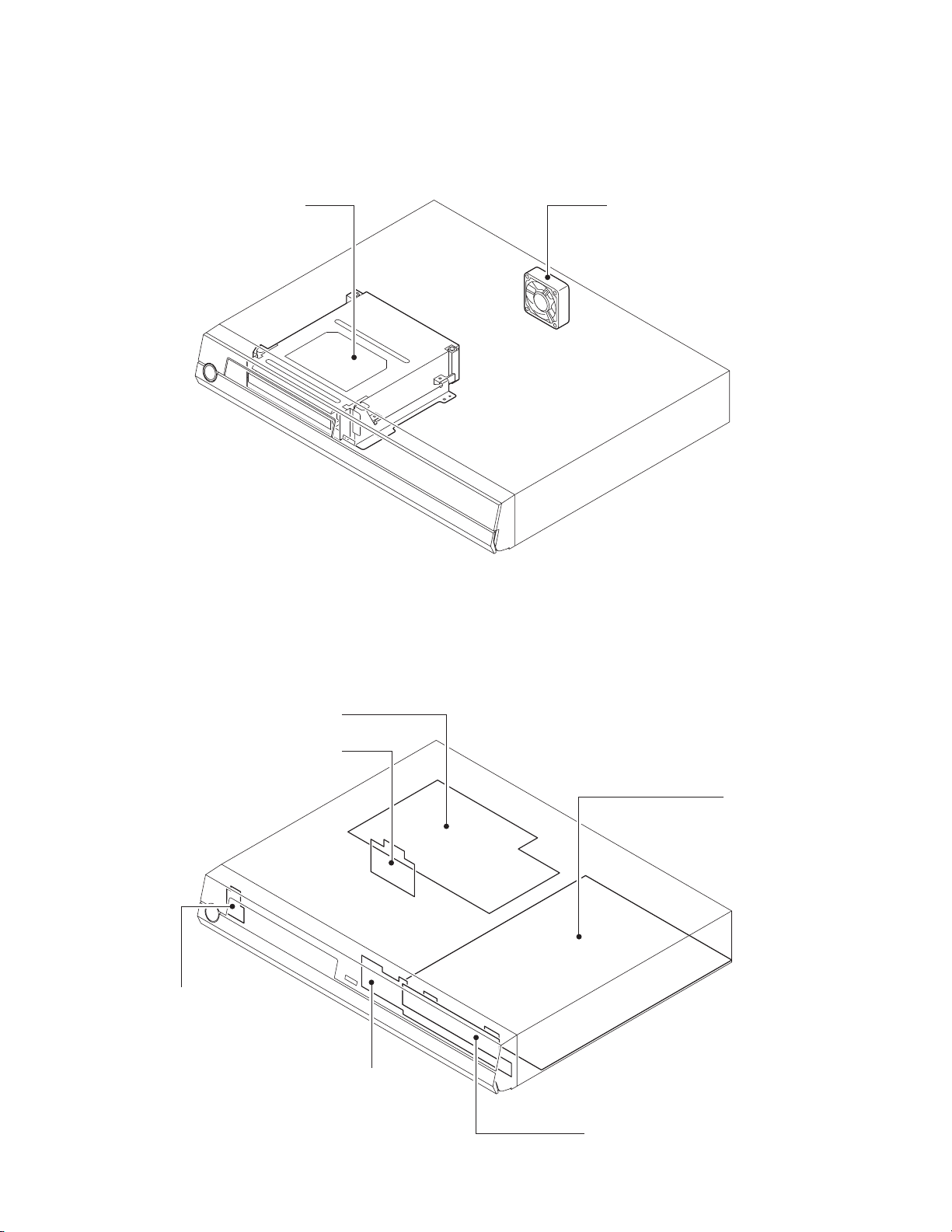
2. LOCATION OF MAIN PARTS
2-1. Location of Main Parts
DVD DRIVE
FAN
Fig. 1-2-1
2-2. Location of PC Boards
Power PC board
ATAPI PC board
Power switch PC board
Front switch/USB PC board
Main PC board
Fig. 1-2-2
Front FIP PC board
SECTION 2
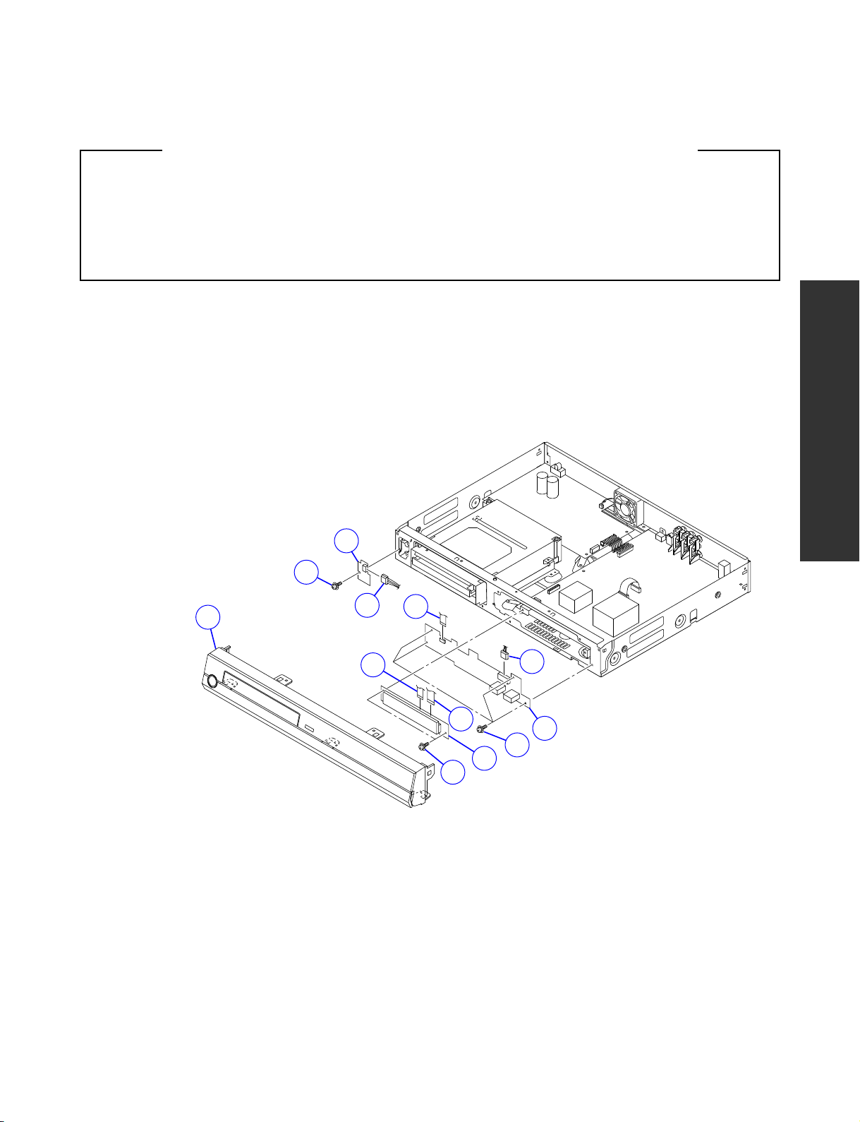
PART REPLACEMEANT PROCEDURES
CAUTIONS BEFORE STARTING PART REPLACEMENT
Electronic parts are susceptible to static electricity and may easily damaged, so do not forget to ground as required.
Many screws are used inside the unit. To prevent the screws from missing or dropping, etc. always use a magnetized
screwdriver in servicing. Several kinds of screws are used and some of them need special cautions. That is, take care of
the tapping screws securing molded parts and fine pitch screws used to secure metal parts. If they are used improperly,
the screw holes will be easily damaged and the parts can not be fixed.
1. REPLACEMENT OF MECHANICAL PARTS
Note:
• Circled numbers in the figure show the main disassembly procedure. Refer to them when disassembling.
• This section describes how to replace the parts of HD-A2KU as a representative.
1-1. Front Panel, Front PC Boards
CHASSIS OF MAIN PARTS
SECTION 2
POWER SWITCH PC BOARD
FRONT PANEL
4
3
1
2
5
8
9
5
11
FRONT SWITCH/USB PC BOARD
10
7
6
FRONT FIP PC BOARD
Fig. 2-1-1
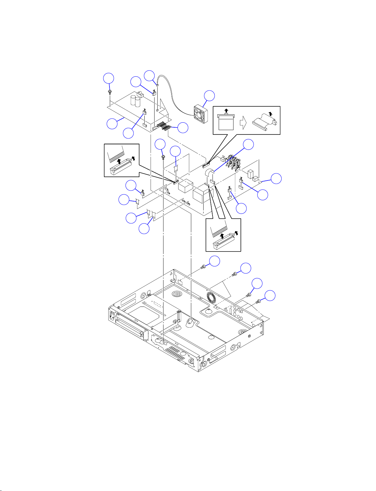
1-2. Main/Power PC Boards
POWER PC BOARD
6
8
2
4
FAN
3
5
4
11
9
9
12
MAIN PC BOARD
10
9
10
10
9
9
Fig. 2-1-2
1
1
7
7
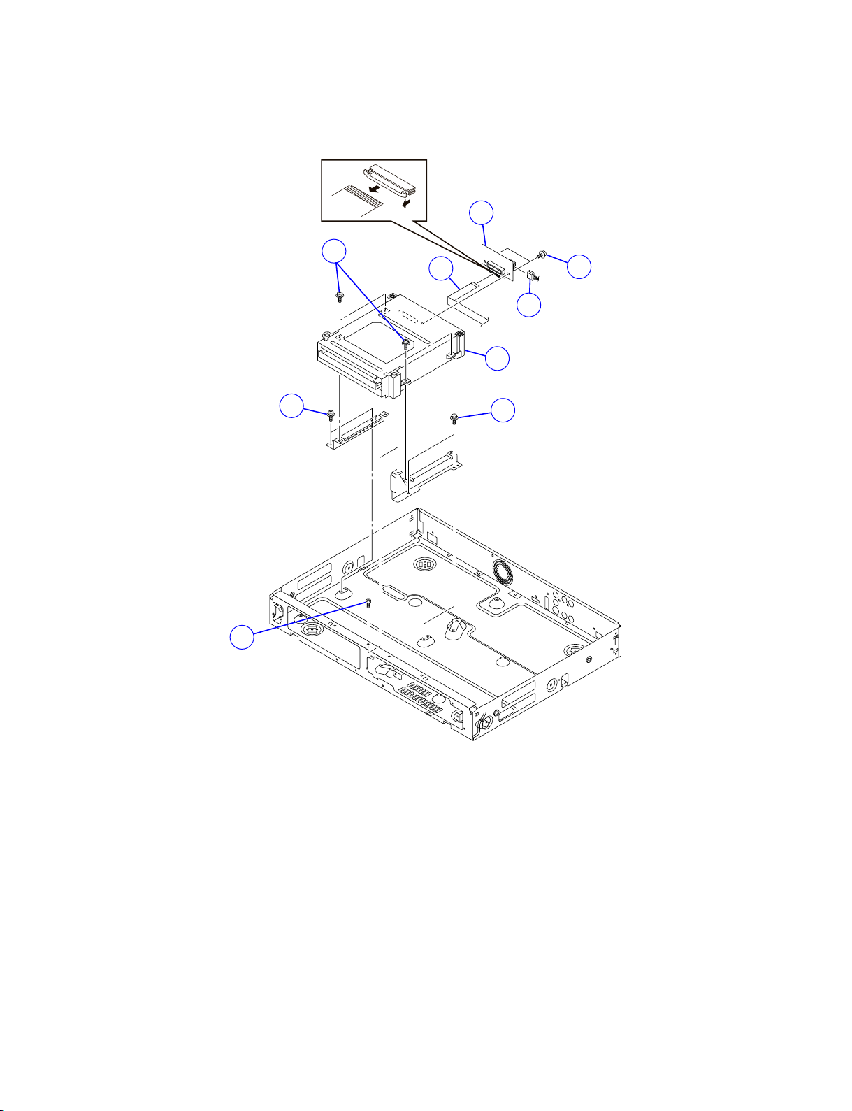
1-3. DVD Drive
ATAPI PC BOAD
5
6
2
4
3
7
DVD DRIVE
1
1
1
Fig. 2-1-3

2. WIRING CONNECTION DIAGRAM
After the servicing is complete, return the wiring to its original state by using the diagram below as a reference.
FANW102 W104
Main PC board
Power PC board
ATAPI PC board
W004
W101
W103
Power switch PC board
Front panel
: Tape
: Flexible cable
DVD DRIVE
W001
Front FIP PC board
Fig. 2-2-1
W002
Front switch/USB PC board
W003

SECTION 3
SERVICING DIAGRAMS
1. CIRCUIT SYMBOLS AND SUPPLEMENTARY EXPLANATION
1-1. Precautions for Part Replacement
• In the schematic diagram, parts marked (ex.
F801) are critical part to meet the safety regulations, so
always use the parts bearing specified part codes (SN)
when replacing them.
1-2. Solid Resistor Indication
Unit None ........... Ω
K ........... kΩ
M ........... MΩ
Tolerance None ........... ±5%
B ........... ±0.1%
C ........... ±0.25%
D ........... ±0.5%
F ........... ±1%
G ........... ±2%
K ........... ±10%
M ........... ±20%
Rated Wattage (1) Chip Parts
None .........1/16W
(2) Other Parts
None .........1/6W
Other than above, described in the Circuit Diagram.
Type None ........... Carbon film
S ........... Solid
R ........... Oxide metal film
M ........... Metal film
W ...........Cement
FR ........... Fusible
• Using the parts other than those specified shall violate
the regulations, and may cause troubles such as
operation failures, fire etc.
Eg. 1
100k
Rated Wattage Type Tolerance
Fig. 3-1-1
SERVICING DIAGRAMS
1-3. Capacitance Indication
Symbol
Unit None ........... F
Rated voltage None ........... 50V
Tolerance (1) Ceramic, plastic, and film capacitors of which
Temperature characteristic None ........... SL
(Ceramic capacitor) For others, temperature characteristics are
Static electricity capacity Sometimes described with abbreviated letters as
(Ceramic capacitor) shown in Eg. 3.
+
........... Electrolytic, Special electrolytic
NP
........... Non polarity electrolytic
........... Ceramic, plastic
M
........... Film
........... Trimmer
µ ...........µF
p ........... pF
For other than 50V and electrolytic capacitors,
described in the Circuit Diagram.
capacitance are more than 10 pF.
None ........... ±5% or more
B ........... ±0.1%
C ........... ±0.25%
D ........... ±0.5%
F ........... ±1%
G ........... ±2%
(2) Ceramic, plastic, and film capacitors of which
capacitance are 10 pF or less.
None ........... more than ±5 pF
B ........... ±0.1 pF
C ........... ±0.25 pF
(3) Electrolytic, Trimmer
Tolerance is not described.
described. (For capacitors of 0.01 µF and
no indications are described as F.)
Eg. 2
100µ
Temperature
response
Rated
voltage
Tolerance
Fig. 3-1-2
Eg. 3
104
4
pF (0.1µF)
10x10
Temperature characteristic
(or Temperature characteristic+
Static electricity capacity tolerance)
Fig. 3-1-3
SECTION 3

1-4. Inductor Indication
Unit None ........... Η
µ ...........µH
m ...........mH
Tolerance None ........... ±5%
B ........... ±0.1%
C ........... ±0.25%
D ........... ±0.5%
F ........... ±1%
G ........... ±2%
K ........... ±10%
M ........... ±20%
1-5. Waveform and Voltage Measurement
• The waveforms for CD/DVD and RF shown in the
circuit diagrams are obtained when a test disc is
played back.
• All voltage values except the waveforms are expressed
in DC and measured by a digital voltmeter.
1-6. Others
• The parts indicated with "NC" or "KETU" etc. are not
used in the circuits of this model.
Eg. 4
Type name
Fig. 3-1-4
Eg. 5
10µ
Type Tolerance
Fig. 3-1-5

2. PRINTED WIRING BOARD AND SCHEMATIC DIAGRAM
PWR_
SW UNIT
FAN
LEADS
CABLE
1
2
FL+5V
GND
POWER
Ritgh Angle
CN101
E+5V
GND
1
2
3
4
GND
123456789
Power_LED
Power_Key
2.0mmLtype
W002
FFC
123456789
W103
GND
WIRE
CN702
1 44 4 4
2 55 5 5
3 66 6 6
4
CN801
PS_ON
VCC+3.3V
GND
VCC+3.3V
B+5V
VCC+5V
GND
E+6V
GND
VCC+12V
GND
VCC+12V
GND
VCC+12V
GND
E+5V
GND
VEE-5V
GND
FL+5V
1.5mmBB
CN804 CN3001 38 38 38 38
VCC+12V 1
VCC+12V 2
GND 3
GND 4
CN802
GND
GND
2mmStype
11 12 12 12 12
22 13 13 13 13
33 14 14 14 14
44 15 15 15 15
55 16 16 16 16
66 17 17 17 17
77 18 18 18 18
88 19 19 19 19
99 20 20 20 20
10 10 21 21 21 21
11 11 22 22 22 22
12 12 23 23 23 23
13 13 24 24 24 24
14 14 25 25 25 25
15 15 26 26 26 26
16 16 27 27 27 27
17 17 28 28 28 28
18 18 29 29 29 29
19 19 30 30 30 30
20 20 31 31 31 31
Vkk
21 21 32 32 32 32
22 22 33 33 33 33
-F
23 23 34 34 34 34
W104
12V
12V
5V
5V 12V
WIRE
1 46 46
2 47 47
3 48 48
4
5
6
CN601
1.5mmBB 35 35 35 35
1
2
3
4
FIP UNIT
D_LIGHT_LED
SG18
SG17
SG16
SG15
SG14
SG13
SG12
SG11
SG10
1011121314151617181920
SG6
SG9
SG5
SG8
SG7
SG1
SG4
SG3
SG2
CN105 CN104 CN102 CN103
+F
1.0mm type 1.0mm type 1.0mm type
Ritgh Angle Ritgh Angle Ritgh Angle Ritgh Angle
14G
14G
14G
14G
14G
14G
-F
123456789
14G
14G
14G
14G
14G
10111213141516
14G
14G
14G
GND
W003
FFC
1011121314151617181920
SG14
SG13
SG12
1.5mmStype
SG11
SG10
SG6
SG5
SG9
SG4
SG8
SG7
SG3
SG15
SG18
SG17
SG16
E+5V
Power_LED
Power_Key
GND
PS_ON
VCC+3.3V
GND
VCC+3.3V
B+5V
VCC+5V
GND
E+6V
GND
VCC+12V
GND
VCC+12V
GND
VCC+12V
GND
E+5V
GND
VEE-5
V
GND
FL+5V
Vkk
+F
-F
VCC+12V 39 39 39 39
VCC+12V 40 40 40 40
GND 0.5mmStype 0.5mmStype 41 41
GND 42 42
CN706 CN705 CN703
1mmStype 1mmStype 1mmStype
SG2
SG1
+F
123456789
14G
14G
14G
14G
-F
14G
10111213141516
14G
14G
14G
14G
14G
14G
14G
MAIN
14G
14G
GND
EJECT-SW
123456789
W001
FFC
123456789
EJECT-SW
D_LIGHT_LED
CVBS/YUVX
S3
K2
E1
S2
E1
S2
K1
CVBS/YUVX
S3
K2
K1
SW_USB UNIT
EVER5V
GND
GND
R/C
101112
101112
EVER5V
GND
GND
R/C
W101
WIRE
GND
123456789
123456789
GND
D2+
D1+
D2-
D1-
GND
VDD
VDD
VDD
D1+
D1-
GND
VDD
D2+
D2-
CN403 CN001
B_DRESET
B_DMAREQ
B_DMAC
(Gold) 44 44
W102
WIRE
SHIELD
2.0mmLtype
SHIELD
CN402
1.5mmStype
D_GND
B_DD7
B_DD8
B_DD6
B_DD9
B_DD5
B_DD10
B_DD4
B_DD11
B_DD3
B_DD12
B_DD2
B_DD13
B_DD1
B_DD14
B_DD0
B_DD15
D_GND
NC
D_GND
B_DIOW
NC
B_DIOR
D_GND
B_IORDY
NC
D_GND
B_INTRQ
NC
B_DA1+F
NC
B_DA0
B_DA2
B_CS0
B_CS1
B_DASP
D_GND
W004
FFC
11 1 1
22 2 2
33 3 3
77 7 7
88 8 8
99 9 9
10 10 10 10
11 11 11 11
K
36 36 36 36
37 37 37 37
B_DRESET
D_GND
B_DD7
B_DD8
B_DD6
B_DD9
B_DD5
B_DD10
B_DD4
B_DD11
B_DD3
B_DD12
B_DD2
B_DD13
B_DD1
B_DD14
B_DD0
B_DD15
D_GND
NC
B_DMAREQ
D_GND
B_DIOW
NC
B_DIOR
D_GND
B_IORDY
NC
B_DMACK
D_GND
B_INTRQ
NC
B_DA1
NC
B_DA0
B_DA2
B_CS0
B_CS1
B_DASP
D_GND
ATAPI
ADAPTOR
CN003
1
12V
2
GND
3
GND
4
5
5V
5V
6
2mmStype
CN002
EJECT_SW
TRAY_STATUS
NC
GND
RESETX
DD8
DD7
DD9
DD6
DD10
DD5
DD11
DD4
DD12
DD3
DD13
DD2
DD14
DD1
DD15
DD0
DNARQ
GND
DIORX
DIOWX
GND
IORDY
DMACKX
INTRQ
NC
DA1
NC
DA0
CS0X
CS1X
DASPX
5V
5V
5V
5V
5V
GND
GND
GND
GND
12V
12V
12V
12V
43 43
45 45
49 49
50 50
HD-DVD
EJECT_SW
TRAY_STATUS
NC
GND
RESETX
DD8
DD7
DD9
DD6
DD10
DD5
DD11
DD4
DD12
DD3
DD13
DD2
DD14
DD1
DD15
DD0
DNARQ
GND
DIORX
DIOWX
GND
IORDY
DMACKX
INTRQ
NC
DA1
NC
DA0
DA2DA2
CS0X
CS1X
DASP
X
5V
5V
5V
5V
5V
GND
GND
GND
GND
12V
12V
12V
12V
Fig. 3-2-1

3. BLOCK DIAGRAMS
L
k
K
Front Unit
Thermal Sensor
ADM1032AR
Celeron M
900MHz
0 Cash
100MHz
FSB400MHz
Power Suplly
256MB
DDR
SDRAM
GMCH
FW82854
DDR333
Hublink
ATA
IDE Con.
SST
32MB
NAND-FLASH
256Mb*1
14.31318MHz X'tal
Clock Gene.
ICS950812
100MHz
48MHz 33MHz
ICH4-M
48MHz
33MHz
33MHz
FW82801DBM
EXT
32.768KHz
LAN
Controllor
RLT8100C
25MHz
33MHz
24.576MHz
32MB
NOR-FLASH
256Mb*1
P
C
I
B
U
48MHz
S
33MHz
USB HOST
Controllor
uPD720102G
256MB
NAND-FLASH
2Gb*1
EMI BUS
FWH
RJ45
PWRGOOD HDMI
PWRON VXO
E+5V
E+6V
VCC+12V
VEE-5V
VCC+3.3V
Vk
F+
FCPU+5V
HEADER*2
HD-DVD
ATA
EMMA3
PCICL
PCI
SYSTEM CLOCK
EMI
EJTAG interface
N-Wire interface *2
(Vr5500 and V850)
Video output - CY/CB/CR
Video output - SY/SC
IEC60958 Output
16bit
32bit DDR2
DDR2
SDRAM interface
SDRAM
256MB
DDR2 SDRAM
1Gb*2
UART1
UART
SPI
AIOMCK0
DAO0[0-4]
BCK,LRC
DVO0
IIC1
IIC0
256MB
DDR2 SDRAM
512Mb*4
3.3V<->5VTrans.
ADSP
21262
256kb
EEPROM
32.768KHz
232C(8pin)
JTAG(10pin)
N-Wire(TP only)
20MHz
XO
XO
Audio DAC
PCM1755
JTAG(10pin)
3.3V<->5VTrans.
Timer
uCOM
78F0535
Video
Driver
MM1757
Buffer
OP Amp
NJM4580
HDMI Tx
SiI9030
COAXAL
OPTICA
FL
FL
Driver
COMPONENT
S VIDEO
COMPOSITE
DM 2chL
DM 2chR
USB*2
REM
Fig. 3-3-1

4. CIRCUIT DIAGRAMS
4-1. Power Supply Circuit Diagram
4-1-1. Power Supply Circuit Diagram (Type A)
Note : In the power supply circuit, two kinds (type A and type B) are, and are compatible.
Fig. 3-4-1

4-1-2. Power Supply Circuit Diagram (Type B)
Fig. 3-4-2

4-2. Front Circuit Diagram
4-2-1. Front FIP Circuit Diagram
Fig. 3-4-3

4-2-2. Power Switch Circuit Diagram
Use
Not use
Fig. 3-4-4

4-2-3. Front Switch/USB Circuit Diagram
Do vout guard at GND.
Use
Not use
Not use
Not use
Fig. 3-4-5

4-3. ATAPI Conversion Circuit Diagram
Fig. 3-4-6

4-4. Main Circuit Diagram
4-4-1. AV Output Circuit Diagram
Note : The main circuit diagrams describe only part of information.
FROM EMMA3
IEC958_SEL
IEC958
DIT_CSX
RESET1X
DIT-INT_X
DIT-BLS
DIT-CDOUT
DSPO_PB-BCK
DSPO_DATA-DM
DSPO_PB-LRCK
EA29
FROM DSP
DSPO_BCK
DSPO_LRCK
DSPO_I2S(IEC958)
FROM DSP
RA40
22
RA41
22
RA42
100
22
RA57
RA43
100
RA45
100
RA44
100
F0.1u
P3V
LA02
MPZ2012S331AT
RA47
RA59
22
RA46
22
CA32
FROM EMMA3
SDO
SCK
DAC_CSX1
AMCK
ICA04
TC7WH241FU
0
1
VCC 8
2
RA48
36
22
4
GND
1
NC
2
CDOUT
3
CCLK
4
CDIN
5
CS_X
6
MCLK
7
Vio
8
DGND
9
RXP
10
NC
11
SCLK
12
SYNC
13
SDATA
14
NC
ICA05
DIT4069
F0.1u
7
RA49
5
28
MODE
27
U
26
NC
25
BLS
24
NC
23
NC
22
INT_X
21
NC
20
NC
19
Vdd
18
TX+
17
TX-
16
DGND
15
RST_X
FROM TIMER
EA14
EA13
EA16
VEE2
COUT
VSAG
VOUT
YSAG
YOUT
VCC2
VEE2
VEE2
GND
VEE
CA13
B0.022u
EV11
EA17
CA14
RA15
5.1kD
47uF16V
CA15
FL1200p
CA17
NC(CH820p)
CA18
100uF16V
EA18
GND
CA16
RA16
5.1kD
47uF16V
CA20
NC(CH820p)
EV19
ICV02
MM1565AF
1
2
3
CV05
F2.2u(2012)
CV17
100uF16V
CV12
100uF16V
CV18
RV48
F2.2u(2012)
CV34
NC(1005)
CV02
F0.1u
CV36
NC(1005)
CV04
F0.1u
CV38
NC(1005)
CV03
F0.1u
CV40
NC(1005)
CV13
F0.1u
CV11
F0.1u
CV41
NC(1005)
NC
28
27
26
25
24
23
22
FIN2
RV43
0
21
LV02
NC(1608)
20
19
18
17
16
15
4
CV14
CV16
100uF16V
F0.1u
CV15
F2.2u(2012)
GND
CV22
CV27
CV29
NC(1005)
NC(1005)
NC(1005)
CV26
CV28
CV30
NC(1005)
NC(1005)
NC(1005)
RA14
100
EA11
PCM1755
RV38
NC(1608)
0
EA15
100
RA12
RA13
100
EA12
16
SCK
15
ML
14
MC
13
MD
12
ZL
11
ZR
10
Vcom
9
AGND
ICA02
CA12
10uF16V
P5V
E+6V
VCC+12V
VEE-5V
EV08
1
CIN
2
Mute1
3
VIN
4
YCMIX
5
YIN
6
BIAS
0
7
VCC1
LV01
VEE
FIN1
8
RV49
CYIN
0
9
D/S
CBIN
SD/HD
CRIN
MUTE2
VEE1
MM1757BHBE
ICV01
CYOUT
CYSAG
CBOUT
CROUT
10
11
12
13
14
RA11
22uF16V
NC(1005)
NC(1005)
F0.1u
100
EA10
1
BCK
2
DATA
3
LRCK
4
DGND
5
NC
6
VCC
7
LOUT
8
ROUT
CA11
EV12
CV19
F0.1u
CV01
F0.1u
CV20
F0.1u
CV08
CV09
F0.1u
CV33
CV06
F0.1u
CV32
CV21
F0.1u
RV36
0
RV14
100
RV37
CV07
F0.1u
CV31
NC(1005)
GND
RA09
RA10
100
RA08
100
100
JA01
F0.1u
(NC)
LAF1001-0901F
GND
CA04
RA02
(NC)
VCC
Vin
a
b
EA05
GND
EA04
(NC)
EA06
RA03
100
33
RA04
CA05
22
(NC)
(NC)
NC
RA05
150
CA06
B1u
EA07
RA06
12k
RA07
10k
1
VIN
VOUT
2
GND
3
CNTL
ICA01
MM1575ANRE
EA09
5
EA08
CA08
4
NSBYP
CA07
F0.1u
B1u
CA09
100uF16V
CA10
100uF16V
GND
GND
EV01
EV02
EV03
QV02
2SC2712Y
RV01
330k
RV02
1M
RV03
NC
QV05
NC
RV04
0
RV10
NC
RV12
0
RV13
100
RV15
NC
RV16
100
RV17
NC
RV18
100
RV19
NC
RV05
22k
RV06
10k
RV08
470k
RV20
NC
QV06
NC
RV22
NC
QV07
2SC2712Y
RV24
2.2k
QV08
2SC2712Y
RV44
2.2k
QV09
2SC2712Y
RV45
2.2k
RV11
3.3k
2SC2712Y
QV04
CV10
F0.1u
DV01
1SS355
EV06
DV02
1SS355
EV10
DV03
1SS355
EV09
EV07
DV04
1SS355
EV05
SY-OUT
EV04
SC-OUT
CY-OUT
CB-OUT
CR-OUT
RV09
100
RV07
100
RV35
NC
RV50
NC
EA02
LA01
MMZ1608S601CT
CA01
NC(F0.1u)
EA01
RA01
QA01
2SC2712Y
100(NC)
(NC)
RA58
100
2SA1162Y
(NC)
CA33
22
EA32
EA31
22
RA55
EA30
10k
RA50
0
RA56
10k
RA51
RA54
10k
CA34
4.7uF10VTANTAL(NC)
2
3
GND
CNTL
NSBYP
4
CA35
F0.1u
CA36
F0.1u
CA02
F0.1u
EA03
CA03
F0.1u
(NC)
QA02
RA53
EA33
12k
RA52
10k
CA37
F1u
1
VIN
ICA06
EA34
MM1575ANRE
VOUT
5
CA38
F0.1u
GND
FROM DIGITAL
VMUTE-CVS
VMUTE1
VMUTE-YUV
S1_ASP1
Sel_I/P
D_ASP_OUT
RESOLUTION
RA17
2.2k
NC(F0.1u)
RN1402
VO
VIN
NC
SUB
GND
CN
EA19
CA21
CA19
FL1200P
RA20
100
QA04
CONT
RA18
5.6kD
RA19
5.6kD
EA20
1SS355
CA23
1000uF10V
RA22
100
GND
7
6
5
CV23
F1u
EV24
EV22
EV25
EV23
RA23
7.5kD
DA01
7.5kD
RA21
VSS
CA22
CH180p
CH180p
4
GND
EA21
CA24
QA03
RN2402
VCC
1236
857
47uF16V
QA05
RN2402
EA22
CA25
EA23
ICA03
NJM4580
CA26
F0.1u
DA02
1SS355
FRONT_MUTE
FROM TIMER
47uF16V
CA27
B0.022u
RA24
47kD
CA28
RA26
47kD
EA27
RA35
RA30
EA28
470D
RA28
RA34
680D
470D
FL1200p
QA07
EA25
HN1C03
6
RA29
2.2k
RA31
1M
CA31
680D
FL1200p
RA39
CA29
2345
1
470k
RA37
470k
EV20
JV01
EV34
EV44
EV33
EV45
EV47
EV27
EV35
EV36
EV28
EV30
EV29
EV32
EV31
EV48
EV38
EV39
EV40
EV41
EV42
EV43
EV54
EV55
EV56
EV57
EV58
EV59
EV60
D1/D2/D3/D4
D GND
MSP-864V1-03_NI_LF
JV03
YKF-45-3011
1
2
3
4
5
6
7
8
9
10
11
12
13
14
14
13
12
11
10
9
8
7
6
4
2
1
3
5
Y-OUT
Y-GND
PB-OUT
PB-GND
PR-OUT
PR-GND
NC
LINE1(1080/720/480)
LINE2(P/I)
NC
LINE3(16:9/LB/4:3)
DET GND
NC
INSERT DET
CY
Rch
CB
Lch
CR
CV
S-C
S-Y
CV37
F0.1u
RV40
8.2k
RV41
1.8k
75F(1608)
RV34
75F(1608)
75F(1608)
RV31
75F(1608)
CV42
F0.1u
RV28
75F(1608)
RV30
RV32
75F(1608)
RV39
75F(1608)
RV42
75F(1608)
75F(1608)
CV39
F0.1u
RV29
RV33
CV43
F0.1u
EV26
CV25
F0.1u
CV24
100uF16V
RV23
12k
RV21
10k
EV21
EV18
RV26
10k
RV27
1.8k
RV25
1.8k
CV35
F0.1u
Fig. 3-4-7

4-4-2. Timer Circuit Diagram
E704
E705
E711
E713
E712
CN701
1
5vcpu
TimwerReset
WriteEnable
52808-1071
2
3
4
GND
TxD
RxD
3State
GND
E701
CTS
RXD
TXD
RTS
E708
5
6
E709
7
8
33
9
10
R705
E710
10k
R708
E707
E702
33
R704
33
R707
E703
E706
R702
33
33
R706
1
2
3
4
5
6
7
R710 33
R701
C701
IC701
GND
CD74HCT125A
R780
R782
VOUT
22k
R783
22k
E753
VDD
E754
GND
IC704
F0.1u
PST3222
MMZ1608S601
C726
C724
47uF16V
FL+5V
L707
MMZ1608S601
C745
F0.1u
R719
4.7K
BZ01
R748
10k
ONVCC-M5P
S1_ASP1
Sel_I/P
E773
E771
GND
4
Power_Key
3
Power_LED
2
E+5V
1
CN702
B4B-ZR-SM4-TF(LF)(SN)
E720
E721
E722
C715
E723
1K
E+5V
E714
E715
1
5
10
R718
12
100
100p
E778
1k
CH15p
CH15p
C706
E+5V
R727
R738
R740
R742
15
34
10uF16V
C705
EVdd
100
14
Vdd
FANRQ-M5N
35
C707
F0.1u
12
13
Vss
EVss
uPD78F0535GB
Yobi1
Yobi2
36
37
10k
10k
10k
R751
R752
R755
C704
10uF16V
10K
10K
10K
10K
33
16
E+5V
RSTREQ-M5N
F0.1u
14
VCC
13
12
11
10
9
8
100p
C702
R709
10k
SHRST-M5N
RSMRST-M5N
PWRBTN-M5N
R716
10K
KBRST-M5N
USBON0-M5P
USBOC0-P5N
USBOC1-P5N
POWER_ON0
FRONT_MUTE
THRM-M5N
POWER_GOOD
R720
R734
R735
R736
R737
R739
R711
R777
R784
R712
R717
E765
100
R779
D_ASP_OUT
RESOLUTION
100
100
100
100
33
33
100
33
10K
100
33
MMZ1608S601
MMZ1608S601
17
18
19
20
21
22
23
24
25
26
27
28
29
30
31
32
100p
L701
L702
SHRST-M5N
RSMRST-M5N
PWRBTN-M5N
KBRST-M5N
NC
USBON0-M5P
USBOC0-P5N
USBOC1-P5N
RTS(T-E)
CTS(E-T)
D-Light-LED
PWR_ON0
HMUTE
(NON)PONOK-M5P
THRM-M5N
Eject-SW
Power-SW
33
R724
C721
C703
X701
AT-41-20M
1M
R725
0.47u
REGC
PSON-M5P
38
10k
R753
C709
470
PWPON_M5P
Power_Good
39
100
R754
PWPON-M5P
2.2u(2012)
C708
40
C710
CH18p(1608)
X702
SP-T2A
R726
10k
R728
8
9X210X111
XT27XT1
FLMD0
IC700
SP_OUT
RESOLUTION41RxD(E-T)42TxD(T-E)43PWROK-M5P
R730
R729
8.2k (1608)
8.2k (1608)
C711
2.2u(2012)
820k
6
CH22p
10k
R732
5
RESET
44
R723
100
PWROK-M5P
C712
R731
3
4
VMUTE1
FLASH_OWE
AV_RxD
45
46
R714
R715
10K
10K
2
SLP3-M5N
DRU_OUT(T-D)
AV_TxD
AVref
47
R741
1
P-CORE
REMOTE
BUZZER
PWR_LED
DRI_CS
DRI_IN(D-T)
DRISCK
ONVCC_M5P
S1_ASP
SEL_I/P
VMUTE2
CVBS/YUVX
P12V_SEN
P3V_SEN
AGND
48
RTC_OUT
CEC
P5V_SEN
MMZ1608S601
L703
F0.1u
C713
VCC3.3V
100
64
63
62
61
60
59
58
57
56
55
54
53
52
51
50
49
R744
R703
R771
R785
R759
R762
R773
R733
R713
R743 100
R750 100
R772 100
E+5V
F0.1u
C714
P_CORE
VMUTE1
E772
100
100
100
100
100
100
100
E716
C722
B0.01u
100
100
SLP3-M5N
CLK_32K
D702
1SS355
ON/OFF+5V
E774
E775
E776
E777
EJECT-SW
D-Light-LED
CVBS/YUVX
EVER5V
52808-1271
S1
S2
S3
K2
K1
R/C
CN703
PS1240P02AT
E719
CPU+5V
L704
47uF16V
R7461K
R7561K
R757
CPU+5V
E726
E727
E728
E729
E730
E731
E732
E733
E734
E735
E736
C729
F0.1u
B0.01u(1608)
C718
C719
F0.1u
1
2
3
R721
R722
4
5
1K
6
1K
R745
7
82k(1608)
8
9
10
11
12
13
1SS355
D705
VKK
C720
E739
E738
49
50
51
52
VEE
VDD
GND
CLK
DIN
STB
DOUT
K1
K2
OSC
GND
VDD
SG1
SG2
SG3
SG4
SG5
14
IC705
PT6324_Q(L)
SG615SG716SG817SG918SG1019SG1120SG1221SG1322SG1423SG1524SG16
R77833
R77633
R77533
R77433
R77033
R76933
42
40
39
GR7
GR841GR9
GR1043GR1144GR1245GR1346GR1447GR1548GR16
GR6
38
GR5
37
GR4
36
GR3
35
GR2
34
GR1
33
SG24
32
SG23
31
SG22
30
SG21
29
SG20
28
SG19
27
SG18
SG17
26
25
R76833
R76733
R76633
R76533
R76433
R76333
R76133
R76033
E745
E744
E743
E742
E741
E740
1
D704
1SS383
E737
E763
E764
ON/OFF+5V
E748
E749
E750
E751
E752
E755
E758
E759
E761
E762
E767
E768
E769
E760
L706
B0.01u
C730
MMZ1608S601
C732
F0.1u
E757
E717
E718
C733
100uF16V
C735
F0.1u
-F
E724
E725
CN705
52808-1671
1
F-
14G
13G
12G
5
11G
10G
9G
8G
7G
10
6G
5G
4G
3G
2G
15
1G
16
CN704
E746
E747
52808-2071
1
2
3
4
5
6
7
8
9
10
11
12
13
14
15
16
17
18
19
20
E766
+F
VCC+5V
E+6V
E756
R78622K
15K
10K
C716
100p
R749
C717
100p
10K
R788
R787
100uF16V
C741
C744
F0.1u
VCC+12V
E770
DGND
47k
R781
Fig. 3-4-8

A
134
2 5
5. PC BOARDS
5-1. Front FIP PC Board
B
C
D
1234
A
Fig. 3-5-1 Front FIP PC Board (Top side)
1234
A
Fig. 3-5-2 Front FIP PC Board (Bottom side)
CN104CN105
A100
W173
E
F
G
5-2. Power Switch PC Board
Fig. 3-5-3 Power Switch PC Board (Top side)
Fig. 3-5-4 Power Switch PC Board (Bottom side)
S115
C118
R102
D121
D122
R146
R147
R101
CN101
Q102
Q101

5-3. Front Switch/USB PC Board
5-4. ATAPI PC Board
12345
CN103
W103
A
J101 J102
Fig. 3-5-7 ATAPI PC Board (Top side)
W172
C119
IC102
S102
S103
S107
S109 S116
CN102
A
S100
S104
CN106
S108
Fig. 3-5-5 Front Switch/USB PC Board (Top side)
12345
12
12
C101
R148
C100
L101
R105
A
L105
R108
FL101
L104
R107
L103
R106
FL102
L102
R104
R149
RJ01RJ02
R103
Fig. 3-5-6 Front Switch/USB PC Board (Bottom side)
RJ03
R110
C112
A
Fig. 3-5-8 ATAPI PC Board (Bottom side)

SECTION 4
PARTS LIST
SAFETY PRECAUTION
The parts identified by ! ( ) mark are critical for safety. Replace only with part number specified.
The mounting position of replacement is to be identical with originals.
The substitute replacement parts which do not have the same safety characteristics as specified in the parts list may create
shock, fire or other hazards.
NOTICE
The part number must be used when ordering parts in order to assist in processing, be sure to include the model number
and description.
ABBREVIATIONS
Integrated Circuit (IC)
•
Capacitor (Cap)
•
• Capacitance Tolerance (for Nominal Capacitance more than 10pF)
Table 4-2-1
Symbol
Tolerance %B± 0.1
Symbol
Tolerance %
• Capacitance Tolerance (for Nominal Capacitance 10pF or less)
Symbol
Tolerance pF
Resistor (Res)
•
• Resistance tolerance
Symbol
Tolerance %B± 0.1
P
+ 100
0
B
± 0.1
C
± 0.25
Q
+ 30
– 10
C
± 0.25
C
± 0.25
D
± 0.5
T
+ 50
– 10
D
± 0.5
Ex. 10pF G = 10pF ± 2pF
D
± 0.5
F
± 1
U
+ 75
– 10
Table 4-2-2
F
± 1
Table 4-3-1
F
± 1
G
± 2
V
+ 20
– 10
G
± 2
G
± 2
J
± 5
W
+ 100
– 10
J
± 5
K
± 10
X
+ 40
– 20
Ex. 10µF J = 10µF ± 5%
K
± 10
M
± 20
Y
+ 150
– 10
M
± 20
N
± 30
Z
+ 80
– 20
PARTS LIST
SECTION 4
Ex. 470ΩJ = 470Ω± 5%

1. EXPLODED VIEWS 1-1. Packing Assembly
(HD-A2KC) Z006
Z002
Z007
Z005
Z001
(HD-D2KU)
Fig. 4-1-1
Note: The shape of the packing
material is sometimes different.

1-2. Chassis Assembly
B300
RAM1
ATA 1
W004
W102
D
PWR1
A001
PSW1
W103
W003
A001A
W001
FAN1
C
A
B
D
W101
W104
U001
C
A
B
This figure shows the chassis
assembly of HD-A2KU
USB1
W002
FRT1
Fig. 4-1-2

2.PARTS LIST
Location
No.
U001 P000477410 PC BOARD ASSY, MAIN HD-A2KU/A2WKU/D2KU
U001 P000477820 PC BOARD ASSY, MAIN HD-A2KC
PWR1 P000477370 POWER-UNIT, MPN5236
FRT1 P000477360 PC BOARD ASSY, FRONT FIP
PSW1 P000477610 PC BOARD ASSY, POWER-SW
USB1 P000477630 PC BOARD ASSY, FRONT SW/USB
ATA1 P000477350 ATAPI-FFC ADAPTER
A001 P000477390 PANEL ASSY, FRONT HD-A2KU/A2KC
A001A P000477400 DOOR, FRONT HD-A2KU/A2KC
A001 P000477680 PANEL ASSY, FRONT HD-A2WKU
A001A P000477690 DOOR, FRONT HD-A2WKU
A001 P000477710 PANEL ASSY, FRONT HD-D2KU
A001A P000477720 DOOR, FRONT HD-D2KU
Part No. Description
- ELECTRICAL PARTS -
- MECHANICAL PARTS -
B300 P000477380 COVER, TOP
FAN1 P000477470 FAN DC, DSB0512LD-6T10
RAM1 P000477500 HD-DVD-DRIVE, SD-E802A
W001 P000477420 FFC-12P-L102, MAIN-FRONT
W002 P000477430 FFC-20P-L102, MAIN-FRONT
W003 P000477440 FFC-16P-L102, MAIN-FRONT
W004 P000477450 FFC-40P-L242, MAIN-DRIVE
W101 P000477530 WIRE CABLE ZHR-9P-L300, MAIN-USB
W102 P000477540 WIRE CABLE PHR-6P-L100, POWER-ATAPI
W103 P000477550 WIRE CABLE ZHR-4P-L380, MAIN-PWRSW
W104 P000477560 WIRE CABLE PHR-4P-L260, MAIN-POWER
Z001 P000446040 CORD POWER, AC-US
Z002 P000477490 REMOTE CONTROL ,SE-R0252
Z005 P000477620 OWNERS MANUAL, ENGLISH HD-A2KU
Z005 P000477700 OWNERS MANUAL, ENGLISH HD-A2WKU
Z005 P000477730 OWNERS MANUAL, ENGLISH HD-D2KU
Z005 P000477660 OWNERS MANUAL, ENGLISH HD-A2KC
Z006 P000477650 OWNERS MANUAL, FRENCH HD-A2KC
Z007 P000477520 AV CABLE, 3P-L1500 GR

SPECIFICATIONS
Power requirement
Power supply
Mass
External dimension
Signal system
Laser
VIDEO output
S-VIDEO output
COMPONENT output (Y, PB, PR)
ANALOG AUDIO output
DIGITAL AUDIO OUTPUT (BITSTREAM/PCM jack)
LAN port
EXTENSION port
HDMI output
Remote control
Operating conditions
Clock accuracy
• This model complies with the above specifications.
• Designs and specifications are subject to change without notice.
• This model may not be compatible with features and/or specifications that may be added in the future.
• The Illustrations and screens described in this manual may be exaggerated or simplified for easy recognition and may be slightly different from the
actual unit.
33.0W
120V AC 60Hz
4.1kg
Width 430 x Height 65.5 x Depth 345mm
Standard NTSC Color TV system
Semiconductor laser, Wavelength: 405nm/650nm/780nm
1.0Vp-p (75Ω), Sync signal negative, Pin jack x 1 system
(Y) 1.0Vp-p (75Ω), Sync signal negative,
(C) 0.286Vp-p (75Ω), 1 at rear
Mini DIN4 Pin x 1 system
Y output (green), 1.0Vp-p (75Ω), Sync signal negative, Pin jack x 1 system
PB, PR output (blue, red), 0.7Vp-p (75Ω), Pin jack x 1 system each
2.0V (rms), 2.2kΩ or below, pin jack (L, R) x 1 system
Optical connector x 1 system
100BASE-TX/10BASE-T x 1
EXTENSION port x 2 systems
19 pin
Wireless remote control (SE-R0252)
Temperature: 41°F ~ 95°F (5°C ~ 35°C),
Position: Horizontal
Quartz (monthly deviation: approximately ±30 seconds)

1-1, SHIBAURA 1-CHOME, MINATO-KU, TOKYO 105-8001, JAPAN
 Loading...