

Page 1

FILE NO. 2B0-9904
SERVICE MANUAL
CORDLESS TELEPHONE
FT-8939
PUBLISHED IN JAPAN, Sep., 1999
Page 2

CONTENTS
SAFETY PRECAUTIONS ............................................................................................................ 1
OPERATING CONTROLS........................................................................................................... 2
ALIGNMENT PROCEDURE ........................................................................................................ 3
BLOCK DIAGRAMS..................................................................................................................... 9
SCHEMATIC DIAGRAMS..........................................................................................................12
TROUBLESHOOTING HINTS ................................................................................................... 18
IC AND TRANSISTOR VOLTAGE CHART ............................................................................... 25
SEMICONDUCTOR LEAD IDENTIFICATION........................................................................... 31
ELECTRICAL PARTS LOCATION............................................................................................. 34
WIRING DIAGRAMS .................................................................................................................37
EXPLODED VIEW AND MECHANICAL PARTS LIST............................................................... 40
PARTS LIST............................................................................................................................... 44
ASSEMBLY PARTS LIST .......................................................................................................... 60
SPECIFICATIONS ..................................................................................................................... 61
SAFETY PRECAUTIONS
Before returning any models to the customer, a safety check of the entire instrument should be made.
The service technician must be sure that no protective device built into the instrument by the manufacture
has become defective or inadvertently degraded during servicing.
1.WARNING:
Alterations of the design or circuitry of these models should not be made.
Any design changes or additions such as, but not limited to, circuit modifications, auxiliary speaker
jacks, switches, grounding, active or passive circuitry, etc. may alter the safety characteristics of these
models and potentially create a hazardous situation for the user.
Any design alterations or additions will void the manufacturer's warranty and will further relieve the
manufacturer of responsibility for personal injury or property damage resulting therefrom.
2.PRODUCT SAFETY NOTICE
Many electrical and mechanical parts in this chassis have special characteristics. These characteristics
often pass unnoticed and the protection afforded by them cannot necessarily be obtained by using
replacement components rated for higher voltage, wattage, etc. Replacement parts that have these
special safety characteristics are identified in this manual and its supplements; electrical components
having such features are indentified by a in the schematic diagram and the parts list. Before
replacing any of these components, read the parts list in this manual carefully. The use of substitute
replacement parts that do not have the same safety characteristics as specified in the parts list may
create shock, fire or other hazards.
1
Page 3
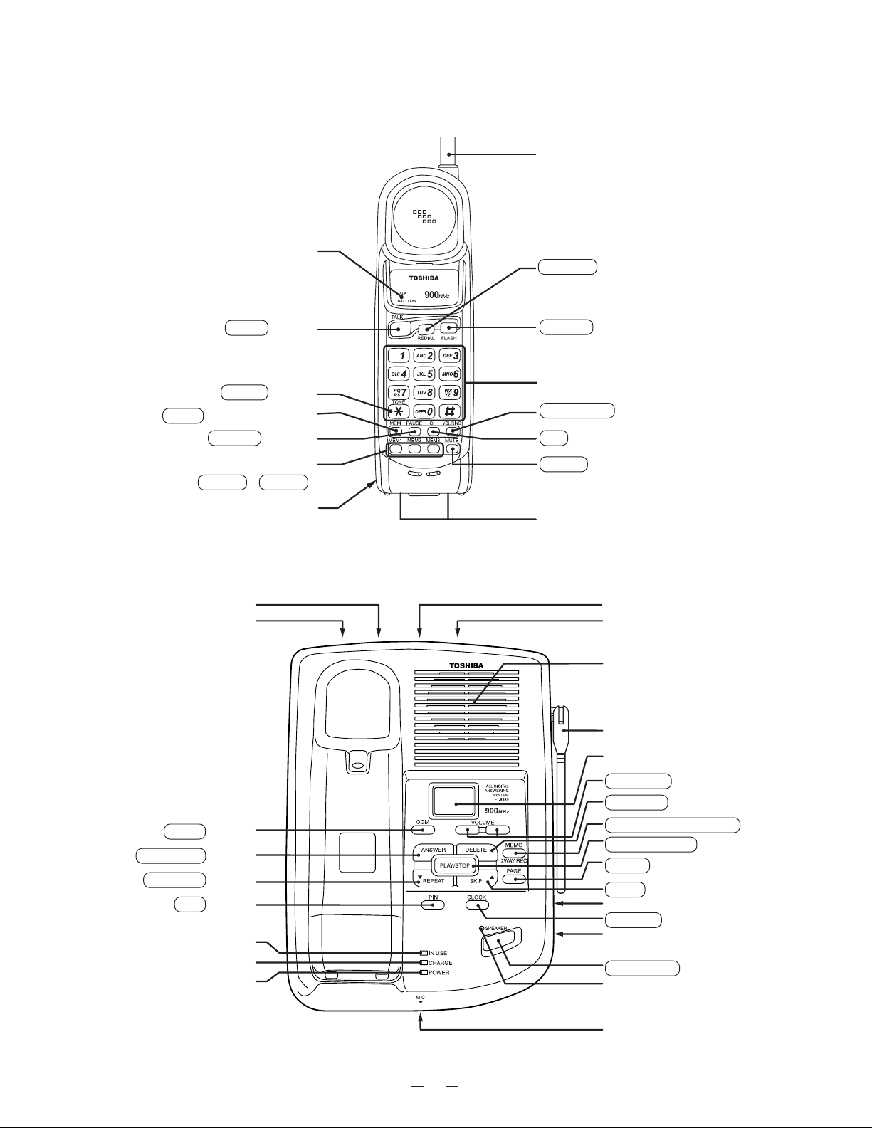
OPERATING CONTROLS
HANDSET CONTROLS AND FUNCTIONS
Antenna
TALK/BATT.LOW LED
TALK Button
TONE Button
MEM (Memory) Button
PAUSE Buttons
One-touch dialing Button
( MEM1 - MEM3 )
Rechargeable Battery Pack
(back)
BASE UNIT CONTROLS AND FUNCTIONS
DC in 9V Jack
TEL LINE Jack
REDIAL Button
FLASH Button
Dialpad (0~9, ∗ and # buttons)
VOL/RING Button
CH Button
MUTE Button
Charging Contacts
T-P(TONE-PULSE) Switch
Ringer ON/OFF Switch
Speaker
OGM Button
ANSWER Button
REPEAT Button
PIN Button
IN USE LED
CHARGE LED
POWER LED
Antenna
LED Display
VOLUME Buttons
DELETE Button
MEMO / 2WAY REC Button
PLAY / STOP Button
PAGE Button
SKIP Button
Rec Time Switch (ANN/4/1)
CLOCK Button
Ring Time Switch (2/4/TS)
SPEAKER Button
Speaker LED
Microphone
2
Page 4
ALIGNMENT PROCEDURE
Test Mode For Base Unit
Press the “PAGE” k ey about 3.0 seconds while turning the power on.
1. To change the TEST mode: Press the “PAGE” key with T/P switch to PULSE position.
2. To change channel: Press the “PAGE” key with T/P switch to TONE position. If changing the step, the
channel returns to the start channel.
3. To cancel Test mode: Bell rings, charge the Handset or Power off.
STEP
1
VCO/TX FRQ. ADJ
2
TX MODE CHECK
3
TX DATA
4
RX SENS.
5
SQ SENS.
6
SINGLE TONE CHECK
7
DUAL T ONE CHECK
8
DATA IN CHECK
9
CHANNEL DATA CHECK
10
*A : CHARGE LED is ON when SQ ON, CHARGE LED is OFF when SQ OFF.
*1 : “0000... ” (250Hz) will be fed out continuously as transmitting data.
*2 : CHARGE LED lights when the received data are “0000...”.
DUPLEX
FUNCTION
START CH
19
19
19
19
19
19
19
19
19
19
TX CONT
L
L
L
H
L
H
H
L
H
L
TX MUTE
L
H
L
L
L
L
L
L
L
H
Channel rotation
19ð20ð21ð40ð1ð25ð2ð3........24ð26........38ð39ð40
RX MUTE
L
L
L
H
*A
L
L
L
L
H
RL CONT
L
H
L
H
H
H
H
L
L
H
REMARKS
*1
*2
3
Page 5
Test Mode For Handset Unit
To Perform the TEST mode, turn the power ON by pressing the “*” and “#” buttons at the same time.
When entered the TEST mode, the bell rings and the unit enters TEST mode 1. (Refer to the follwing table.)
1. To change the TEST mode: Press the number key for the corresponding TEST mode.
(Refer to the follo wing tab le)
2. To change channel: Press “CH” k ey.
(Note: If the step is changed, the channel return to the start channel.)
3. To cancel Test mode: Turn the power OFF, charge the Handset , or press the “TALK” key .
STEP
1
2
3
4
5
6
7
8
9
10
*A : Squelch ON is H, or Squelch OFF is L.
*1 : In the TEST mode 3, “0000...” will be f ed out contin uously as transmitting data.
*2 : In the TEST mode 6, bell (2kHz, 2.2kHz) rings when the data received is “0000...”.
*3 : In the TEST mode 7, bell rings with initial 2 tone (2kHz, 2.2kHz).
*4 : In the TEST mode 8, bell (2kHz, 2.2kHz) rings when P_BATLOW is “L”.
*5 : In the TEST mode 9, bell (2kHz, 2.2kHz) rings when P_CHRGIN is “L”
FUNCTION
VCO/TX FRQ. ADJ
TX MOD . CHECK
TX DATA
RX SENS
SQ SENS
RECEIVE DATA CHECK
BELL
BATTER Y LOW CHECK
CHARGE CHECK
DUPLEX
KEY
1
2
3
4
5
6
7
8
9
0
START CH
21
21
21
21
21
21
21
21
21
21
TX CONT
L
L
L
H
L
L
H
H
H
L
SC
H
H
H
H
H
H
L
L
L
H
TX MUTE
L
H
L
L
L
L
L
L
L
H
RX MUTE
*A
Channel rotation
21ð20ð19ð40ð1ð25ð2ð3........24ð26........38ð39ð40
CONV
L
L
L
H
L
L
L
L
H
H
L
L
L
L
H
H
H
H
L
REMARKS
*1
*2
*3
*4
*5
4
Page 6
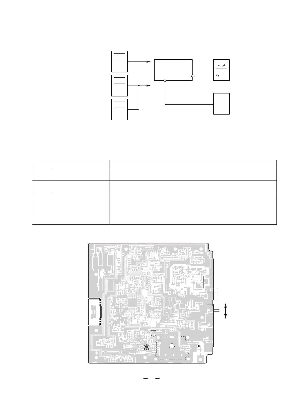
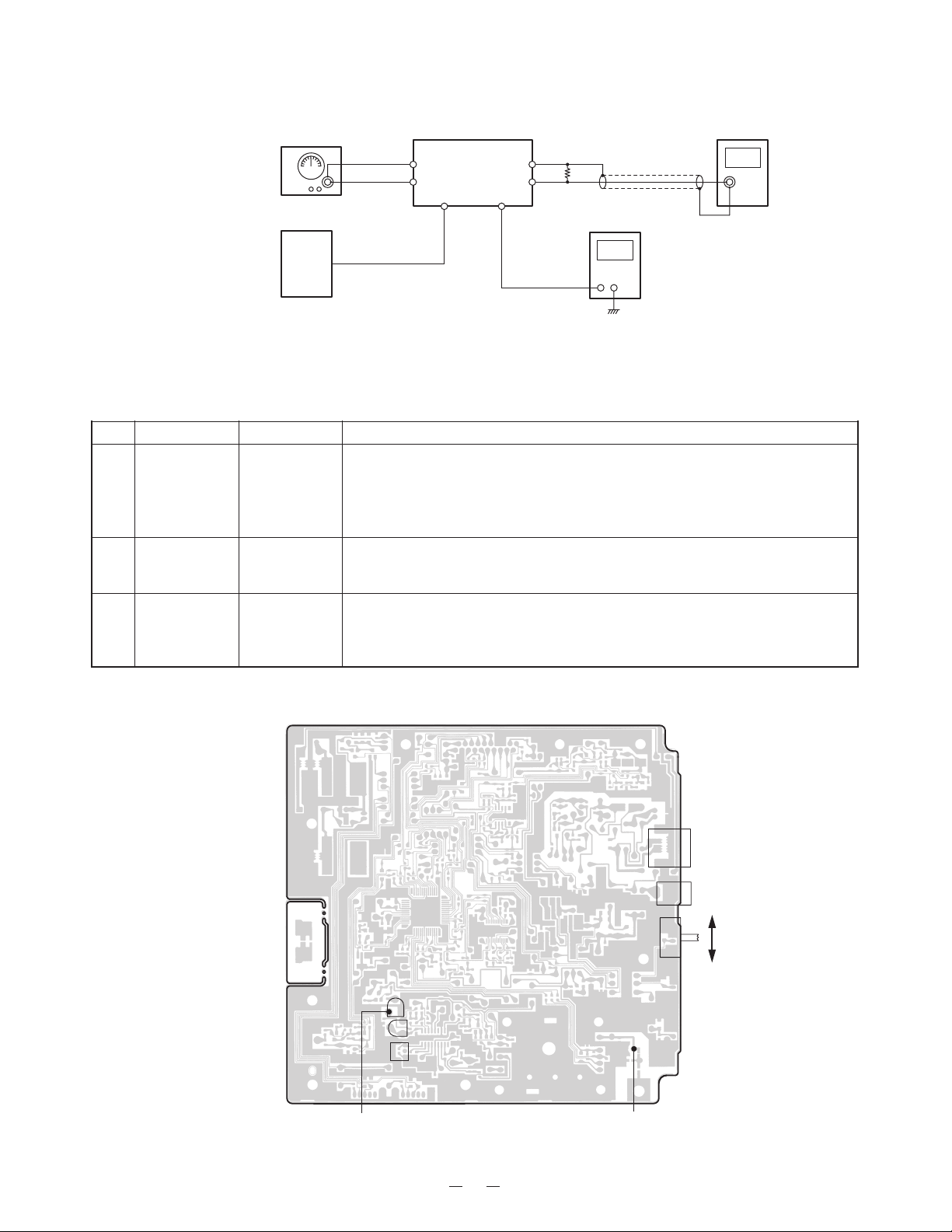
Base Unit
Transmitter Section
Connections
Preset
Place the Base Unit in VCO/TX FREQ.ADJ mode in accordance with the procedure on page 3.
Alignment Procedure
Power
Meter
Frequency
Counter
Deviation
Mater
RF
Test Point
RF
Test Point
BASE Unit
J4
DC IN
9V Jack
TEL Line
Jack
J1
1kHz 77.5mV
AF GEN.
AC
Adapter
AC 120V
60Hz
step
1
2
Adjustment
RT301
(TX P ower)
CT1
(TX Frequency)
Remarks
Connect the Power Meter to the RF test point on the Base MAIN PCB.
Adjust RT301 for a -6.0dBm reading on the Power Meter.
Connect the Frequency Counter to the RF test point on the Base MAIN
PCB. Adjust CT1 to make sure that the frequency is 926.897468 MHz.
Press the “PAGE” k e y to enter the TEST Mode 2. Connect the AF Generator
3
RT3
(TX Modulation)
to the TEL Line Jack on the Base Main PCB. Mak e sure that the output is 1
kHz 77.5 mV from the AF Generator .
Connect the Deviation Meter to the RF test point on the Base MAIN PCB .
Adjust RT3 to indicate ±8 kHz Dev.
Alignment Point Location on Base Main PCB and Base RF PCB
Base Main PCB
J1
TEL LINE Jack
J4
DC IN 9V Jack
T
S2
T/P Switch
P
CT1
RT3
Base RF PCB
RT301
RF Test Point
5
Page 7
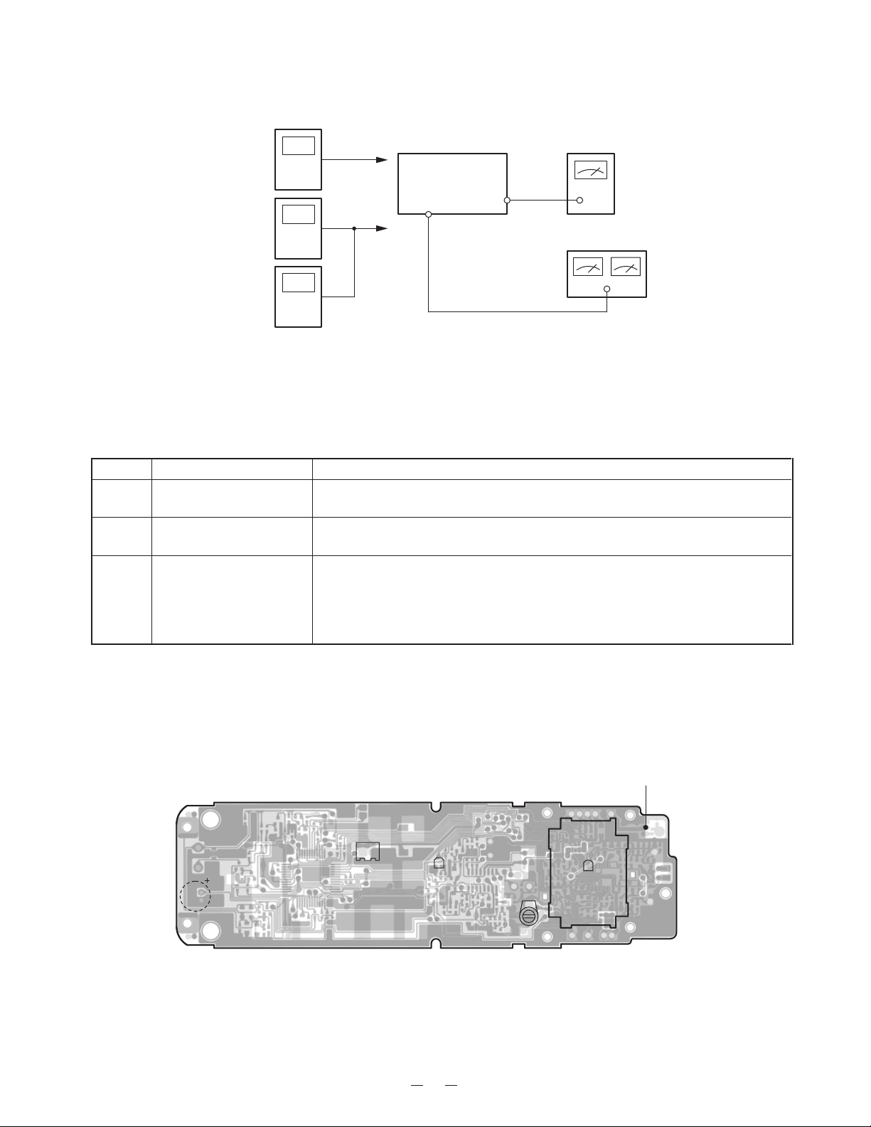
Receiver Section
Connections
RF SG
+
RF
Test Point
TEL Line
Jack
J1
Dummy Load
(600-ohm)
+
AC V oltmeterBASE Unit
AC 120V
60Hz
AC
Adapter
DC IN 9V Jack
J4
AF
Test Point
DC V oltmeter
Preset
Place the Base Unit in RX SENS mode (step 4) in accordance with the precedure on page 3.
Alignment Procedure
step
Preset to
1
SG: 1mV
No modulation
SG: 1mV
2
1 kHz ±8kHz
deviation
SG: -6.0 dB
3
1kHz ±8kHz
Deviation
Adjustment
(Discriminator
Voltage)
(RX AF
Voltage)
µµ
µV
µµ
(SQ Point)
L4
RT2
RT1
Remarks
Connect the RF Signal Generator to the RF test point on the Base MAIN
PCB. Make sure that the frequency is 902.952467 MHz.
Connect the DC Voltmeter to the AF test point. Adjust L4 to indicate DC
1.00 V .
Connect the AC Voltmeter across a 600-ohm dummy to the Telephone Line
Jack. Adjust RT2 for a 245 mV reading on the AC voltmeter.
Press the “PAGE” key to enter the TEST Mode 5. Make sure that the
frequency of RF SG output is 902.952467 MHz. Adjust RT1 to turn to the
point where the bell rings.
Alignment Point Location on Base Main PCB and Base RF PCB
Base Main PCB
RT2
RT1
L4
AF Test Point
RF Test Point
J1
TEL LINE Jack
J4
DC IN 9V Jack
T
S2
T/P Switch
P
6
Page 8
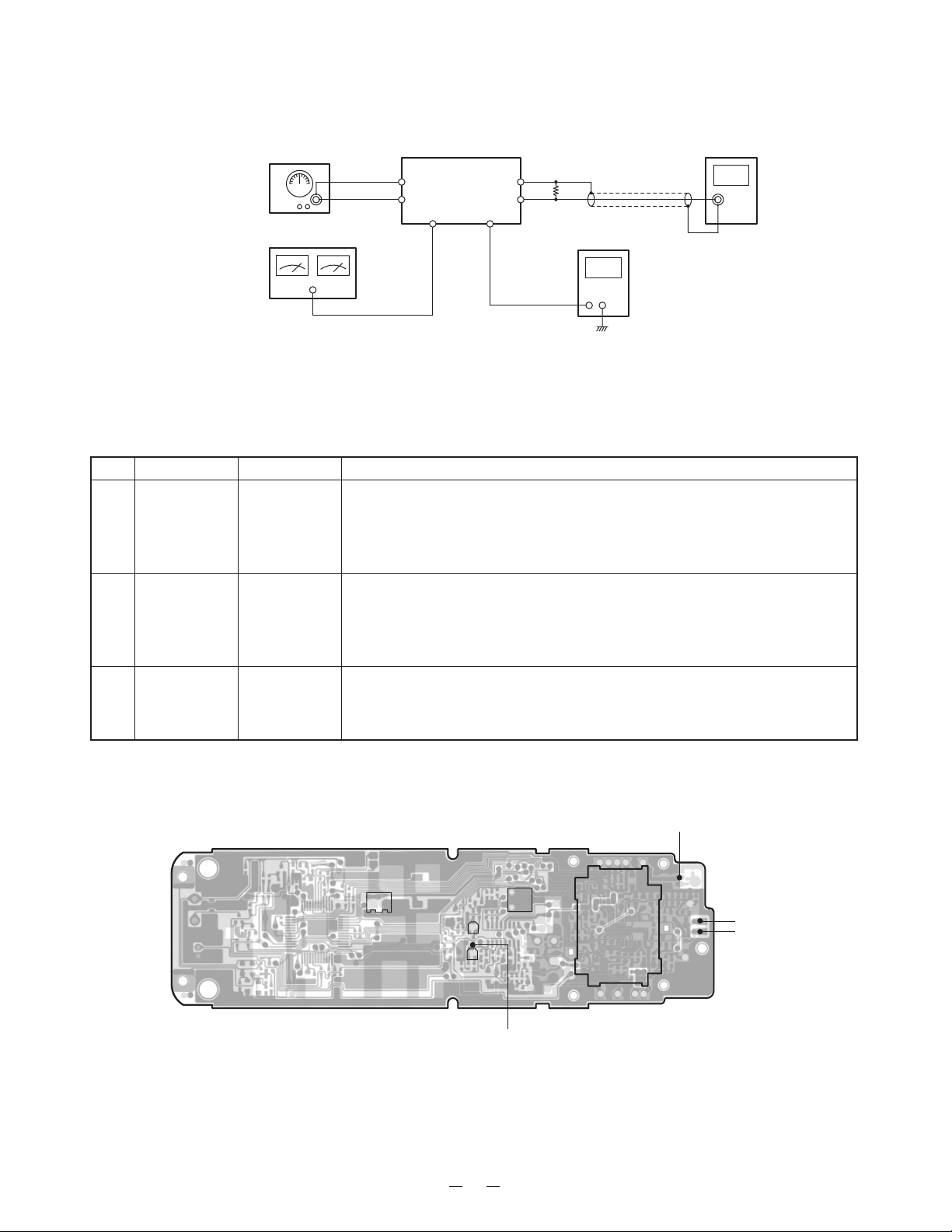
Handset Unit
Transmitter Section
Connection
Power
Meter
Frequency
Counter
Deviation
Mater
RF
Test Point
RF
Test Point
HANDSET Unit
J401
Battery
Connector
MIC+Pin
DC 3.8V
AF GEN.
1kHz 9mV
DC Power Supply
Preset
Place the Handset in VCO/TX FREQ. ADJ mode in accordance with the procedure on page 4.
Alignment Procedure
step
1
2
3
Adjustment
RT501
(TX P ower)
CT401
(TX Frequency)
RT403
(TX Modulation)
Remarks
Connect the RF power Meter to the RF test point on the handset MAIN PCB.
Adjust RT501 for a -7.5dBm reading on the Power Meter.
Connect the Frequency Counter to the RF test point on the handset MAIN
PCB. Adjust CT401 to make sure that the frequency is 903.052467 MHz.
Press the “2” key to enter the TEST Mode 2. Connect the AF Generator to
the MIC Connector. Make sure that the output is 1kHz 9mV from the AF
Generator.
Connect the Deviation Meter to the RF test point on the handset MAIN PCB.
Adjust RT403 to indicate ±8 kHz De v.
Alignment Point Location on Handset Main PCB and Handset RF PCB
Handset PCB
MC401
J401
RT403
CT401
7
RF PCB
RT501
RF Test Point
Page 9
Receiver Section
Connections
RF SG
DC Power Supply
+
Battery
Connector
DC 3.8V
RF
Test Point
J603
Terminal
Dummy Load
SP
+
AF
Test Point
(150-ohm)
DC V oltmeter
Preset
Place the Handset in RX SENS mode (step 4) in accordance with the procedure on page 4.
Alignment Procedure
step
Preset to
1
SG: 1mV
No modulation
SG: 1mV
2
1 kHz ±8kHz
deviation
Adjustment
L402
(Discriminator
Voltage)
RT402
(RX AF
Voltage)
Remarks
Connect the RF Singal Generator to the RF test point on the handset MAIN
PCB. Make sure that the frequency is 926.997467 MHz.
Connect the DC Voltmeter to the AF test point. Adjust L402 to indicate
DC 1.00 V.
Connect the RF Signal Generator to the RF test point on the handset MAIN
PCB. Make sure that the frequency is 926.997467 MHz.
Connect the AC Voltmeter across a 150-ohm dummy to the SP Connector.
Adjust RT402 for a 128 mV (Medium) reading on the AC Voltmeter.
AC V oltmeterHANDSET Unit
SG: -6.0 dB
3
1kHz ±8kHz
Deviation
µµ
µV
µµ
RT401
(SQ Point)
Press the “5” k e y to enter the TEST Mode 5. Make sure that the frequency
of RF SG output is 926.997467 MHz. Adjust RT401 to turn to the point
where the indication is just vibrated.
Alignment Point Location on Handset Main PCB and Handset RF PCB
Handset PCB
J401
L402
RT402
RT401
AF Test Point
RF Test Point
RF PCB
(-)
SP Terminal
(+)
8
Page 10
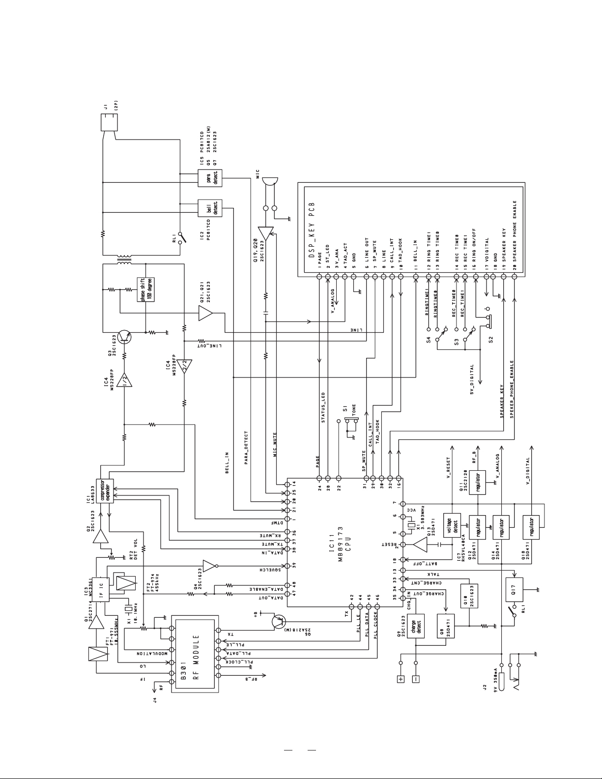
Base Unit, Main
BLOCK DIAGRAMS
9
Page 11
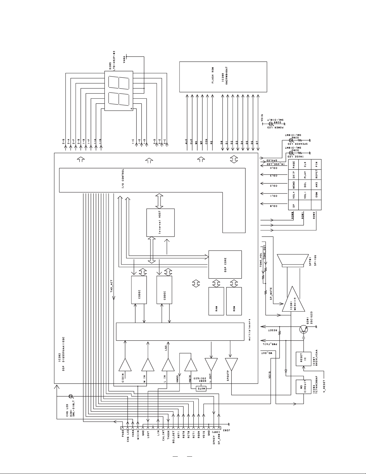
Base Unit, DSP
10
Page 12
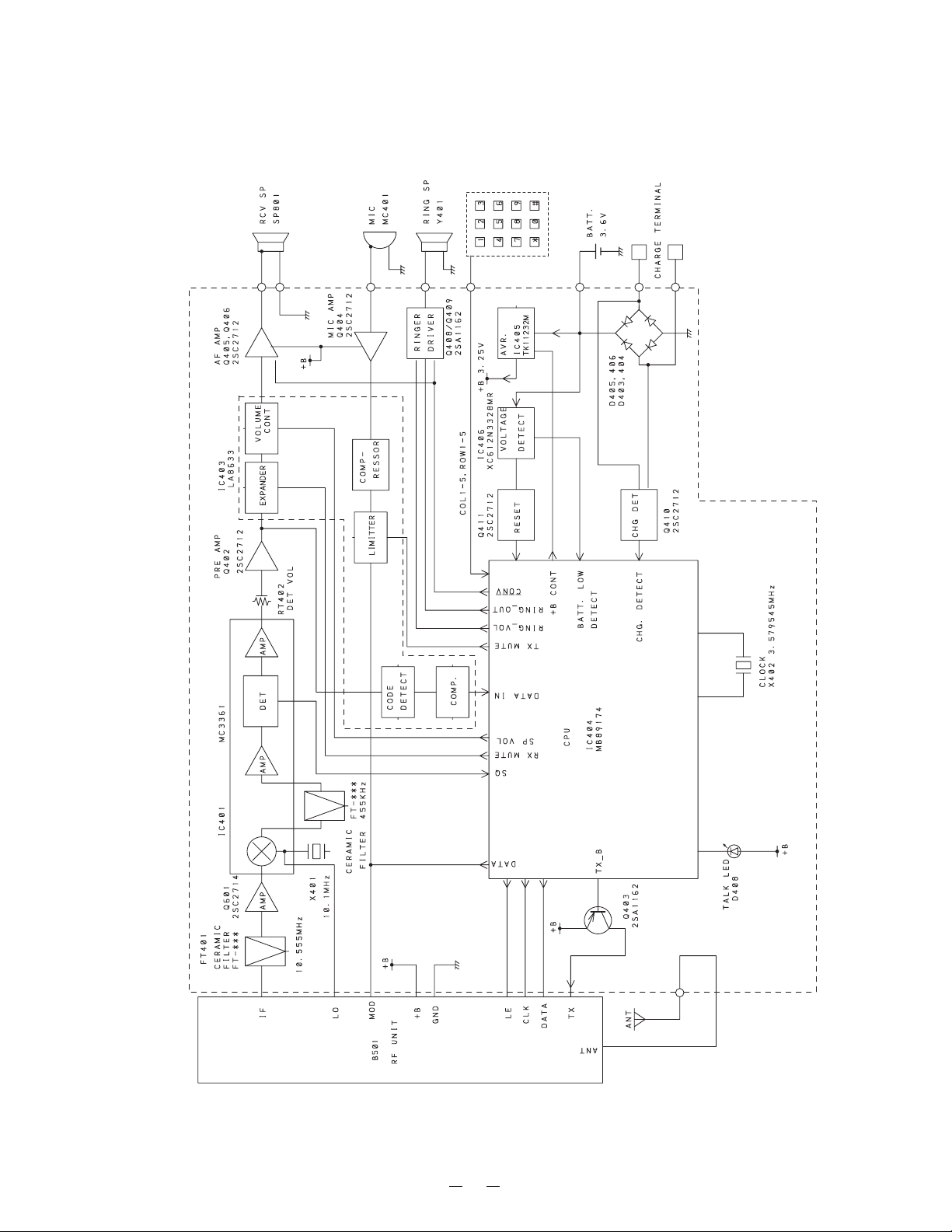
Handset
11
Page 13
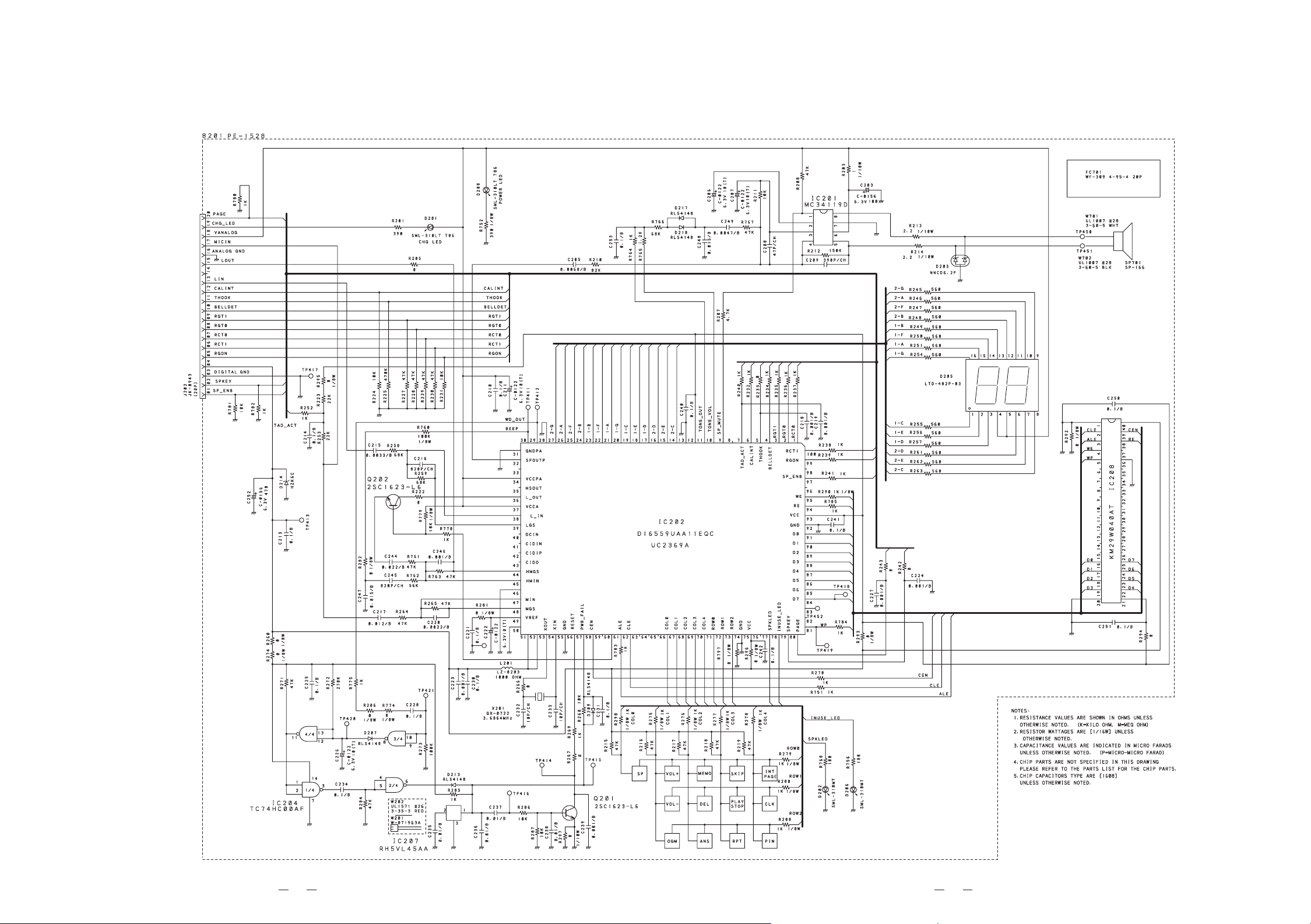
Base Unit, Main
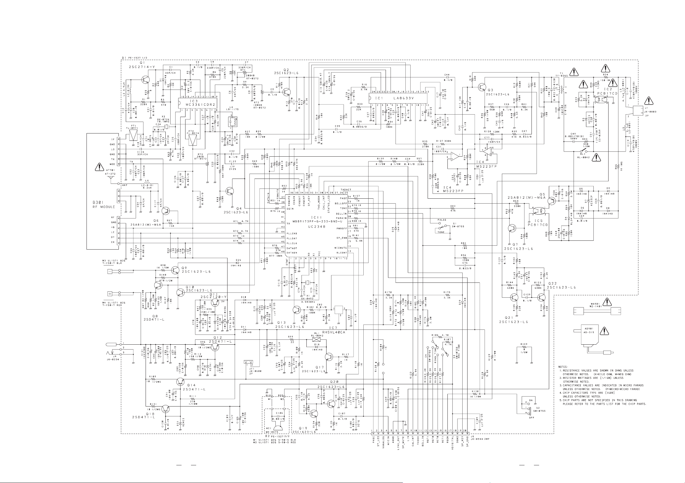
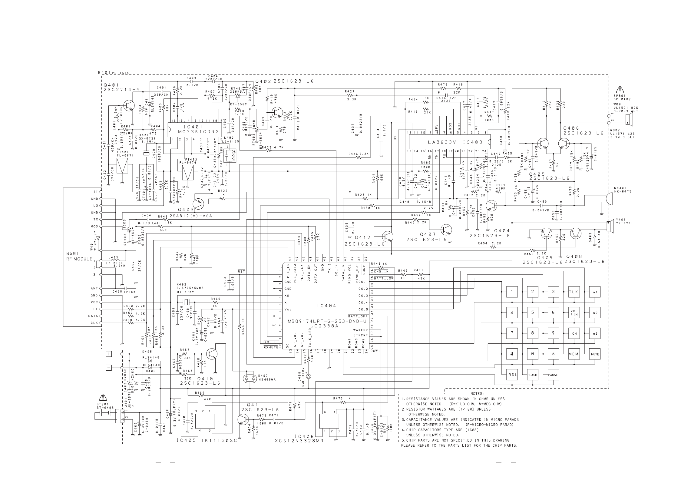
SCHEMATIC DIAGRAMS
12
13
Page 14
Base Unit, Key
14
15
Page 15
Handset
16
17
Page 16

TROUBLESHOOTING HINTS
1. The bell does not ring.
When the PAGE SW of the
base is pressed, does the
ringer on the handset ring?
OK
When the TEL SG is joined
with the base to make bell
signal, is there pulse wave at
pin 4 of IC2?
OK
Is there pulse wave at
pin 21 of IC11?
OK
Check IC11 and its
peripheral circuit.
NG
NG
NG
See 2. The bell does not ring
& page does not ring.
Check IC2 and TEL network
circuit.
Check R78,R82,R94 and
C76.
If you want to reset the unit to the factroy settings
You can cancel the OGM, PIN, and the clock settings by the following process.
1 Disconnect the AC adaptor and telephone line cord from the base. Keep the AC adaptor connected to the wall
outlet. Make sure that the telephone line cord remains disconnected furing this procedure.
2 While pressing the DELETE button, plug the AC power adaptor into the base. Keep pressing the DELETE
button for more than 4 seconds .
A beep sounds and “ P” blinks in the LED display.
To resume using the unit, connect the telephone line cord and place the handset on the base.
Note:
If you turn on the unit again, “ P” may flash.
18
Page 17
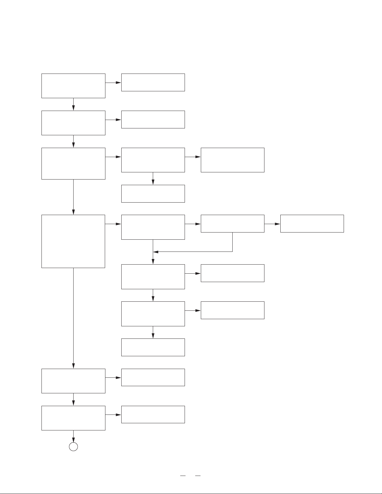
2. The bell does not ring & page does not ring.
Can the base and handset be
connected?
OK
Press handset DIAL key
while in TALK MODE.
Can key touch sound be
heard from the ringer?
OK
When the PAGE SW of the
base is pressed, does pin24
of IC11 change from high to
low?
NG
NG
NG
See 3. The base and handset
cannot be connected.
When the key of the handset is
pressed, can the pulse output
at pin 38 of IC404 be seen?
OK
At the Q408 collector, can the
pulse wave be seen?
OK
Check RINGER Y401.
Check DSP unit.
NG
NG
Check IC404.
Check R454, R457, Q409,
Q408 and D402.
OK
Check IC11 and its peripheral circuit.
19
Page 18
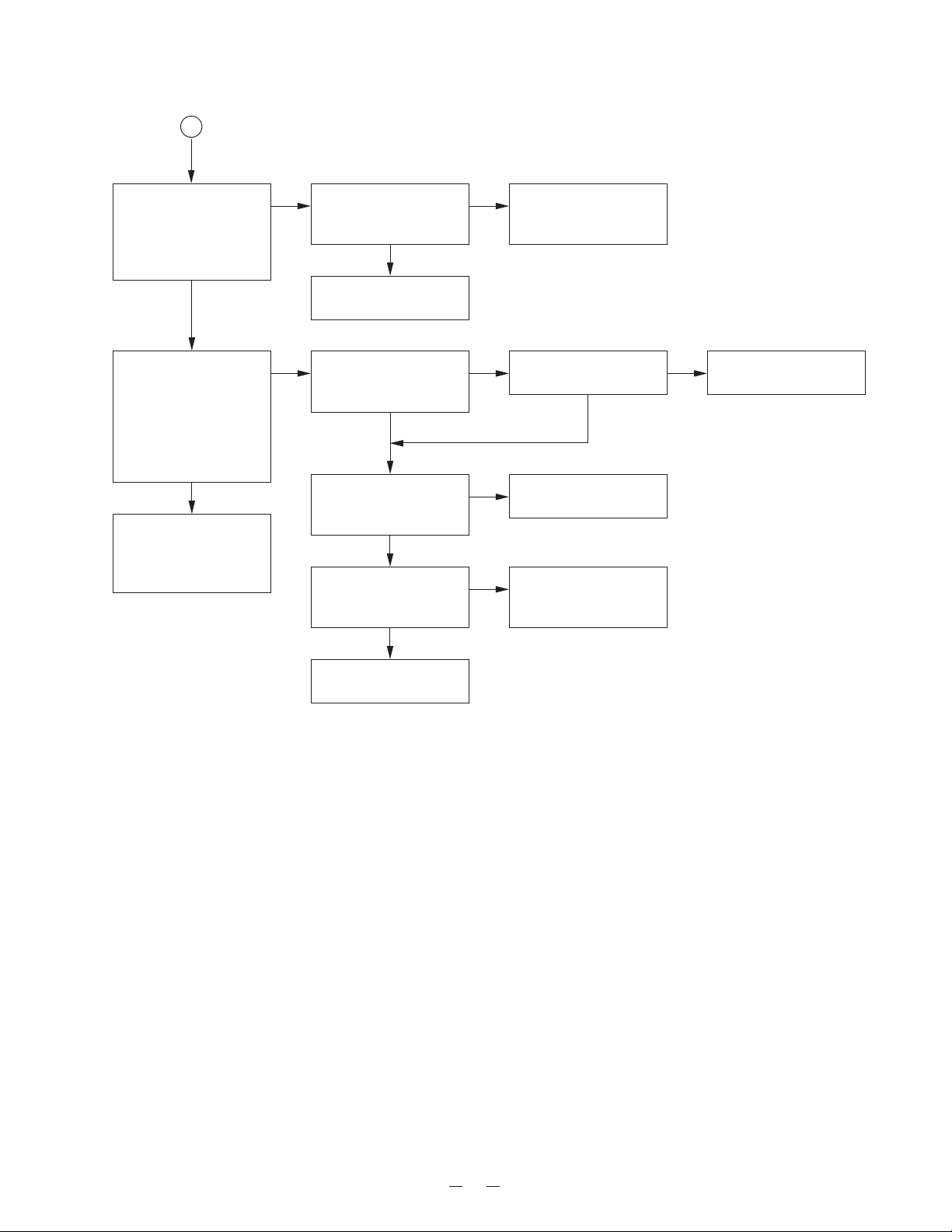
3. The base and handset cannot be connected.
Check whether the base
is able to set in the test
mode 1.
OK
Check the TX POWER
and the TX FREQUENCY
on the base unit.
OK
Set the base in the test
mode 3, check whether
deviation of the TX data
is app. 8.5 kHz Dev.
OK
Set the base in the test
mode 8, 902.952467
MHz (250 Hz ±8 kHz
Dev.) 1mV output signal
from RF test point is
applied. Does the
CHARGE LED light?
OK
NGACheck IC11 and its
peripheral circuit.
NG
Check base RF unit.
Check whether there is a
NG
250 Hz data wavef orm at
“MOD” of RF unit.
OK
Check base RF unit.
NG Check whether there is a
250 Hz data wavef orm at
RT2 AF test point.
OK
Check whether there is a
250 Hz data wavef orm at
the Q2 collector.
OK
Check RT3, R30, R76,
NG
R77, R91, R49, C122,
C33 and C52.
Check IC3, Q1 and their
NG
peripheral circuit.
Check RT2, Q2 and their
NG
peripheral circuit.
OK
NG
Check base RF unit.
Check whether the
handset is able to set in
the test mode 1.
OK
Check the TX POWER
and the TX FREQUENCY
on the handset unit.
OK
Check whether there is a
250 Hz data wavef orm at
pin 38 of IC11.
OK
Check IC11 and its
peripheral circuit.
NG Check IC404 and its
peripheral circuit.
NG
Check handset RF unit.
Check IC1 and its
NG
peripheral circuit.
20
Page 19
A
Set the handset in the
test mode 3, check
whether deviation of the
TX data is app. 8.5 kHz
Dev.
OK
Set the handset in the
test mode 6, 926.997467
MHz (250 Hz ±8 kHz
Dev.) 1mV output signal
from RF test point is
applied. Check whether
the bell ring.
OK
Place the handset on the
base to charge about 5
seconds, then connect
again.
NG Check whether there is a
250 Hz data wav eform at
“MOD” of RF unit.
OK
Check handset RF unit.
Check whether the 250
NG
Hz data waveform from
pin 9 of IC401 is fed.
OK
Check whether there is a
250 Hz data wavef orm at
the Q402 collector.
OK
Check whether there is a
250 Hz data wavef orm at
pin 40 of IC404.
OK
Check RT403, R441,
NG
R442, R443, R444,
R445 and C453.
Check IC401, Q401 and
NG
their peripheral circuit.
Check RT402, Q402 and
NG
their peripheral circuit.
Check R428, R429,
NG
IC403 and their
peripheral circuit.
OK
NG
Check handset RF unit.
Check IC404 and its
peripheral circuit.
21
Page 20

4. Cannot make a phone call (pulse).
Can the base and handset
be connected?
OK
While in TALK MODE, press
dial key of the handset.
Check whether square
waveform from pin 13 of
IC11 is fed.
OK
Check Q17, RL1 and their
peripheral circuits.
NG
NG
See 3. The base and handset
cannot be connected.
Check IC11.
5. Cannot make a phone call (tone).
Can the base and handset be
connected?
OK
NG
See 3. The base and handset
be cannot be connected.
While in TALK MODE, press
dial key of the handset.
Can tone waveform from Pin
1 of IC11 is fed?
OK
Can tone signal be heard
from the handset speaker?
OK
Check the base TEL-line
circuit and RELAY control
circuit.
NG
NG
Check IC11.
Check IC4, Q3 and their
peripheral circuits.
22
Page 21

6. Voice cannot be transmitted to other party (outgoing call).
Can the base and handset be
connected?
OK
The 1 kHz, 9.0mV sine
waveform is applied to
+
MC401
sine waveform from pin 24 of
IC403 be fed?
Check whether there is the
1 kHz sine waveform at
pin 20 of IC403.
Check whether there is the
1 kHz sine waveform at
pin 23 of IC403.
TX output signal from the
handset is detected by the
liner detector, can the 1 kHz
sine waveform be fed?
side, can the 1 kHz
OK
OK
OK
OK
NG
NG
NG
NG
NG
See 3. The base and handset
cannot be connected.
Check Q404 and its
peripheral circuit.
Check IC403 and its
peripheral circuit.
Check RT403 and its
peripheral circuit.
Check handset RF unit.
Check whether there is the
1 kHz sine wave f o rm at pin 9
of IC3 on the base unit.
OK
Check whether there is the
1 kHz sine wave f o rm at pin 3
of IC1.
OK
Check whether there is the
1 kHz sine waveform at
pin 6 of IC1.
OK
Check whether there is the
1 kHz sine waveform at the
Q3 collector.
OK
Check whether the 1 kHz sine
waveform from TEL-line
output is fed.
OK
Check MC401 of handset.
NG
NG
NG
NG
NG
Check IC3, Q1 and their
peripheral circuit.
OK
Check RT2, Q2 and their
peripheral circuits.
Check IC1 and its
peripheral circuit.
Check Q3 and its peripheral
circuit.
Check T1, RL1 and their
peripheral circuits.
NG
Check base RF unit.
23
Page 22

7. The voice of the caller cannot be heard (incoming call).
Can the base and handset be
connected?
OK
The 1 kHz, 77.5mV sine
wavefor m is applied to TELline of the base, can the 1 kHz
sine wavefor m from the Q3
collector be fed?
OK
Check whether there is the
1 kHz sine waveform at
pin 24 of IC1.
OK
Check whether there is the
1 kHz sine waveform at
pin 20 of IC1.
OK
Check whether there is the
1 kHz sine waveform at
“MOD” RF unit.
OK
NG
NG
NG
NG
NG
See 3. The base and handset
cannot be connected.
Check the base TEL-line
circuit and REPLAY control
circuit.
Check Q4 and its peripheral
circuit.
Check C1 and its peripheral
circuit.
Check RT3 and its
peripheral circuit.
TX output signal from the
base is detected by the liner
detector, can the 1 kHz sine
waveform be fed?
OK
Check whether there is the
1 kHz sine wave f o rm at pin 9
of IC401 on the handset unit.
OK
Check whether there is the
1 kHz sine wave f o rm at pin 3
of IC403.
OK
Check whether there is the
1 kHz sine wavefor m at the
pin 18 of IC403.
OK
Check whether there is the
1 kHz sine wavefor m at pin
1, 2 of SP801.
OK
NG
NG
NG
NG
NG
Check base RF unit.
Check IC401, Q401 and
their peripheral circuit.
OK
Check RT402, Q402 and
their peripheral circuits.
Check IC403 and its
peripheral circuit.
Check Q405, Q406 and its
peripheral circuit.
NG
Check handset RF unit.
Check SP801 and W801,
W802.
24
Page 23

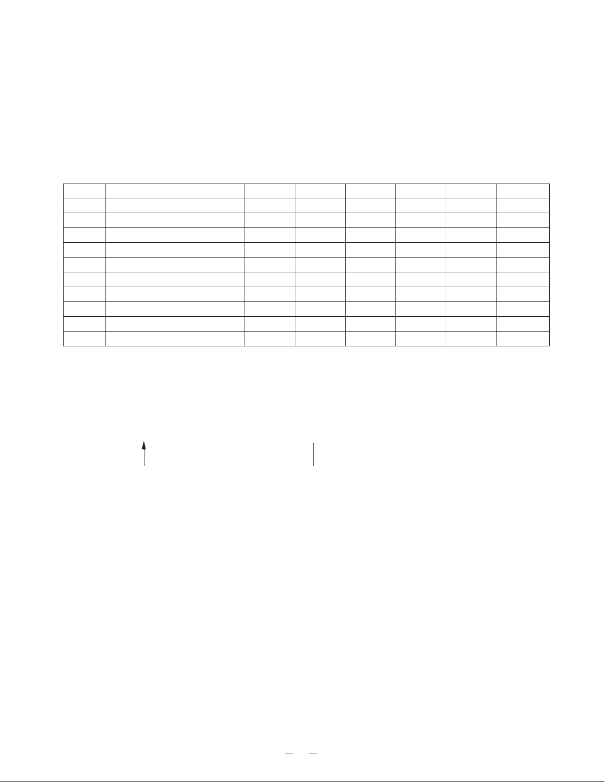
IC AND TRANSISTOR VOLTAGE CHART
Base Unit Unit[V] Unit[V]
Ref. No. PIN STBY TALK NOTE Ref. No. PIN STBY TALK NOTE
1 2.6 2.6
2 2.6 2.6
3 2.6 2.6
4 0.7 0.6
5 2.6 2.6 OPEN
6 2.6 2.6
7 2.6 2.6
8 5.0 5.0 OPEN
9 0 0 GND
10 5.0(AC) 5.0(AC)
11 0 0 GND
12 2.6 2.6
IC1 13 5.0 5.0
14 2.6 2.6
15 2.6 2.6 OPEN
16 0 5.0
17 0 5.0
18 5.0 5.0 OPEN
19 1.4 1.4 OPEN
20 2.6 2.6
21 0.6 0.6
22 2.6 2.6
23 2.6 2.6
24 2.6 2.6
1 0.0 0.0
IC2
IC3 9 1.0 1.0
2 0.0 0.0
3 0.0 0.0
4 4.7 4.7
1 3.1 3.1
2 2.8 2.8
3 3.1 2.8
4 3.2 3.2
5 2.8 2.8
6 2.8 2.8
7 2.8 2.8
8 3.2 3.2
10 0.7 0.7
11 0.7 0.7
12 0.7 0.8
13 3.2 0
14 0 0 OPEN
15 0 0 GND
16 3.2 3.2
IC4 4 0 0 GND
IC5
IC7 2 5.0 5.0
TEL LINE OPEN
TEL LINE OPEN
TEL LINE OPEN
TEL LINE OPEN
IC11 19 0 0 GND
1 2.0 2.0
2 2.0 2.0
3 2.0 2.0
5 2.0 2.0
6 2.0 2.0
7 2.0 2.0
8 5.0 5.0
1 0.0 0.0
2 0.0 0.0
3 0.0 0.0
4 0.6 0.6
1 5.0 5.0
3 0.0 0.0 GND
1 0.0 0.0
2 5.0 5.0
3 0 0 GND
4 0 0 GND
5 3.8(AC) 3.8(AC)
6 5.0(AC) 5.0(AC)
7 5.0 5.0
8 0 0 GND
9 0 0 OPEN
10 0 0 OPEN
11 0 0 OPEN
12 0 0 OPEN
13 0 4.4
14 5.0 5.0
15 0 0 OPEN
16 0 0
17 0 0 OPEN
18 5.0 5.0
20 0 0
21 4.8 4.8
22 5.0 5.0
23 5.0 5.0
24 0.6 0.6
25 1.3 4.0
26 0 0 OPEN
27 2.4 2.4
28 2.4 2.4
29 0 5.0
TEL LINE OPEN
TEL LINE OPEN
TEL LINE OPEN
TEL LINE OPEN
25
Page 24

Unit[V] Unit[V]
Ref. No. PIN STBY TALK NOTE Ref . No. PIN STBY TALK NOTE
30 0.6 0.6
31 0 0 OPEN
32 0.6 0.6
33 5.0 5.0
34 5.0 5.0
35 5.0 5.0
36 0 5.0
37 0 5.0
IC11 38 5.0(AC) 5.0(AC)
39 0 5.0
40 0 0 OPEN
41 0 0 OPEN
42 5.0 0
43 0 0 GND
44 3.2(AC) 3.2
45 3.2(AC) 3.2
46 3.2(AC) 0
47 2.6 2.6
48 0 0
1 2.6 2.6
2 1.4 1.4
3 1.4 1.4
IC201
IC202 9 2.6 2.6
4 1.4 1.4
5 1.4 1.4
6 3.6 3.6
7 0 0 GND
8 1.4 1.4
10 0
20 0
30 0
4 3.1 3.1
50 0
6 0 3.8
7 0 3.8
8 0 0 OPEN
10 0 0
11 0 0
12 3.6 3.6
13 0 0 GND
14 2.2 2.2
15 2.2 2.2
16 2.2 2.2
17 2.2 2.2
IC202 40 0 0 OPEN
18 2.2 2.2
19 2.2 2.2
20 2.2 2.2
21 2.2 2.2
22 2.2 2.2
23 2.2 2.2
24 2.2 2.2
25 2.2 2.2
26 2.2 2.2
27 2.2 2.2
28 0 0 GND
29 3.6(AC) 3.6(AC)
30 0 0
31 0 0 GND
32 1.5 1.5
33 1.5 1.5 OPEN
34 3.6 3.6
35 1.6 1.6 OPEN
36 1.6 1.6
37 3.6 3.6
38 1.6 1.6
39 1.6 1.6
41 0 0 OPEN
42 0 0 OPEN
43 3.6 3.6 OPEN
44 1.6 1.6
45 1.6 1.6
46 0 0 GND
47 1.6 1.6
48 1.6 1.6
49 1.6 1.6
50 0 0 GND
51 3.6 3.6
52 3.6 3.6
53 0.4 0.4
54 0.6 0.6
55 0 0 GND
56 3.6 3.6
57 3.6 3.6
58 3.6 3.6
59 3.6 3.6
60 2.2 0 OPEN
61 0 0
26
Page 25

Unit[V] Unit[V]
Ref. No. PIN STBY TALK NOTE Ref . No. PIN STBY TALK NOTE
62 0 0
63 3.6 3.6 OPEN
64 3.6 3.6 OPEN
65 3.6 3.6 OPEN
66 3.6 3.6
67 3.6 3.6
68 3.6 3.6
69 3.6 3.6
70 3.6 3.6
71 0 0
72 0 0
73 0 0
74 0 0 GND
75 3.6 3.6
76 0 0 OPEN
77 0 0
78 0 3.2
79 0 0
IC202 80 0 0
81 3.6 3.6
82 0 0 OPEN
83 0 0 OPEN
84 0 0
85 0 0
86 0 0
87 0 0
88 0 0
89 0 0
90 0 0
91 0 0
92 0 0 GND
93 3.6 3.6
94 3.6 3.6
95 3.6 3.6
96 0 0 OPEN
97 0 0
98 0 0 OPEN
99 3.0 3.0
100 0.0 0.0
1 3.6 3.6
2 3.6 3.6
IC204 3 0 0
40 0
50 0
IC204 10 3.1(AC) 3.1(AC)
IC207 2 5.0 5.0
IC208 20 0 0 GND
6 3.6 3.6
7 0 0 GND
8 3.6(AC) 3.6(AC)
9 3.1(AC) 3.1(AC)
11 3.6 3.6
12 0.4 0.4
13 0.4 0.4
14 3.6 3.6
1 3.6 3.6
3 0 0 GND
10 0
20 0
30 0
4 3.6 3.6
5 3.6 3.6 OPEN
6 0 0 OPEN
7 0 0 OPEN
8 0 0 OPEN
9 0 0 OPEN
10 0 0 OPEN
11 0 0 OPEN
12 0 0 OPEN
13 0 0 OPEN
14 0 0 OPEN
15 0 0 OPEN
16 0 0
17 0 0
18 0 0
19 0 0
21 3.6 3.6
22 0 0
23 0 0
24 0 0
25 0 0
26 0 0 OPEN
27 0 0 OPEN
28 0 0 OPEN
29 0 0 OPEN
30 0 0 OPEN
31 0 0 OPEN
32 0 0 OPEN
27
Page 26

Unit[V] Unit[V]
Ref. No. PIN STBY TALK NOTE Ref . No. PIN STBY TALK NOTE
33 0 0 OPEN
34 0 0 OPEN
35 0 0 OPEN
IC208 36 0 0 GND
37 0 0 GND
38 3.6 3.6
39 3.6 3.6
40 3.6 3.6
E 0.0 0.0 GND
Q1 C 1.4 1.4
B 0.7 0.7
E 0.3 0.3
Q2 C 2.7 2.7
B 0.9 0.9
E 0.6 0.6
Q3 C 3.8 3.8
B 1.3 1.3
E 0 0 GND
Q4 C 0 5.0
B 0.6 0
E0 0
Q5 C 0 0
B0 0
E 3.2 3.2
Q6 C 0 3.1
B 4.7 2.5
E 0 0 GND
Q7 C 0 0
B 0.6 0.6
E0 0
Q8 C 0 0
B0 0
E0 0
Q9 C 4.8 4.8
B0 0
E 0 0 GND
Q10 C 0 0
B 0.6 0.6
E 3.2 3.2
Q11 C 5.8 5.8
B 3.9 3.9
E 5.8 5.8
Q12 C 8.4 8.1
B 6.4 6.4
Q13 C 5.0 5.0
Q14 C 8.7 8.7
Q17 C 9.0 9.0
Q18 C 8.8 8.3
Q19 C 1.3 1.3
Q20 C 3.9 3.9
Q21 C 2.5 2.5
Q22 C 3 3
Q201 C 3.6 3.6
Q202 C 1.6 1.6
E 0 0 GND
B0 0
E 3.7 3.7
B 4.3 4.3
E0 0
B0 0
E 3.7 3.7
B 4.3 4.3
E 0.1 0.1
B 0.7 0.7
E 0.7 0.7
B 1.3 1.3
E 0.1 0.1
B 0.8 0.8
E 0.3 0.3
B 0.9 0.9
E 0 0 GND
B0 0
E 1.6 1.6
B 2.2 2.2
28
Page 27

Handset Unit[V] Unit[V]
Ref. No. PIN STBY TALK NOTE Ref. No. PIN STBY T ALK NOTE
1 0.0 2.9
2 0.0 2.5
3 0.0 2.5
4 0.0 3.0
5 0.0 2.6
6 0.0 2.6
7 0.0 2.6
IC401 8 0.0 3.0
9 0.0 0.9
10 0.0 0.6
11 0.0 0.7
12 0.0 0.8
13 0.0 0.0
14 0.0 0.0 OPEN
15 0.0 0.0 GND
16 0.0 3.0
1 0-2.0 1.9
2 0-2.0 1.9
3 0-1.5 1.5
4 0-0.4 0.6
5 0-0.4 1.5
6 0-0.4 1.5
7 0-1.8 1.8
8 0.0 3.4
9 0.0 0.0 GND
10 0-3.0 1.6
11 0.0 0.0 GND
IC403 12 0-1.0 1.5
13 0-3.0 3.0
14 0.0 1.5
15 0.0 1.5 OPEN
16 0.0 3.4
17 0.0 3.4
18 0.0 1.5
19 0.0 1.5
20 0.0 1.5
21 0-0.3 0.6
22 0.0 1.5
23 0.0 1.5
24 0.0 1.5
1 0.0 0.0 OPEN
IC404
2 3.5 3.4
3 0.0 0.0 GND
4 0.0 0.0 GND
IC404 27 1.0-3.0 3.4
5 0.0 2.0(AC)
6 0-3.5 2.0(AC)
7 3.5 3.4
8 0.0 0.0 GND
9 0.0 0.0 OPEN
10 0.0 0.0 OPEN
11 0.0 3.4
12 0.0 3.4
13 0.0 3.4
14 0.0 3.4
15 0.0 0.0
16 3.5 0-0.3
17 0.0 0.0 OPEN
18 0.0 0.0 OPEN
19 0.0 0.0 GND
20 0.0 0.0 OPEN
21 0.0 0.0
22 0.0 0.0
23 0.0 0.0
24 0.0 0.0
25 0.0 0.0
26 1.0-3.0 3.4
28 0 0 OPEN
29 3.8 3.8
30 3.5 3.4
31 3.5 3.4
32 3.5 3.4
33 3.5 3.4
34 3.5 3.4
35 3.8 3.8
36 3.8 3.8
37 0.0 3.3
38 0.0 0.0
39 0.0 0.0
40 0-3.0 0-3.0
41 0 0.0
42 0-2.4 0.2
43 0.0 0.0 GND
44 0-0.8 0.8
45 0.0 0.0
46 0-3.0 0.0
47 0-3.0 3.0
48 0-3.0 3.0
29
Page 28

Unit[V] Unit[V]
Ref. No. PIN STBY TALK NOTE Ref. No. PIN STBY TALK NOTE
1 0.0 3.4
2 0.0 0.0 GND
IC405 3 0-1.2 1.2
4 0-3.0 3.0
5 3.8 3.8
1 3.8 3.8
2 3.8 3.8
IC406 3 0.0 0.0 GND
4 3.8 3.8
5 3.8 3.8
E 0.0 0.0 GND
Q401 C 0-2.0 1.7
B 0-0.8 0.7
E 0.0 0.0
Q402 C 0-2.0 1.9
B 0-0.8 0.7
E 0-3.0 3.0
Q403 C 0.0 2.9
B 0-2.4 2.2
E 0.0 0.4
Q404 C 0.0 1.9
B 0.0 1.0
E 0.0 0.5
Q405 C 3.8 2.6
B 0.0 1.2
E 0.0 0.5
Q406 C 3.8 2.5
B 0.0 1.2
E 0.0 0.0 GND
Q407 C 0.0 0.0
B 0.0 0.0
E 0.0 0.0
Q408 C 3.8 3.8
B 0.0 0.0
E 0.0 0.0 GND
Q409 C 0.0 0.0
B 0.0 0.0
E 0.0 0.0 GND
Q410 C 3.8 3.8
B 0.0 0.0
E 0.0 0.0 GND
Q411 C 3.5 3.4
B 0.0 0.0
Q412 C 0-0.5 1.5
E 0.0 3.3
B 0-0.5 1.5
30
Page 29

Base Unit
SEMICONDUCTOR LEAD IDENTIFICATION
D1 /D2 /D5 /D6 /D8 /D9
/D10 /D11 /D16 /D25
/D26 /D28 /D29 /D30 : 1N4148
D3 : HZ7C3
D7 : HZ33CP
D14 : HZ4B1
Anode
D18 : HZ7A1
D31 : HZ4C3
D203 : NNCD6.2F
Anode
Cathode Cathode
Q8 /Q12 /Q14 /Q18 : 2SD471
D4 /D207 /D209
/D213 /D217 /D218 : RLS4148
D15 /D214 : HZK6C
Cathode
Cathode
D205 :LTD-482P
Cathode G1
Cathode A1
16 15 14 13 12 11 10 9
DIGIT 1 DIGIT 2
F1
A1
E1
G1
D1
12345678
Cathode F1
Cathode B1
Cathode B2
B1
F2
C1
E2
Cathode F2
Cathode A2
A2
G2
C2
D2
Anode
Cathode G2
B2
D201 /D208 : SML-310LT
D202 /D206 : SML-310MT
Cathode
Anode
Q1 : 2SC2714
Q2 /Q3 /Q4 /Q7 /Q9 /Q10
/Q13 /Q17 /Q19 /Q20
/Q21 /Q22 /Q201 /Q202 : 2SC1623
Q5 /Q6 : 2SA812(M)
B
E
C
B : Base
E : Emitter
C : Collector
Q11 : 2SC2120
IC1
LA8633VU
E
PRE. IN24
PRE. NF23
1LPF1 IN
2LPF1 OUT
C
B
CMP. NF22
CMP. VREC21
3EXP. IN
4EXT. VREC
CMP. OUT20
LPF2 IN19
LPF2 OUT18
5INT. OUT
6TEL. OUT
7V. HOLD
CMP. MUTE CONT17
EXP. MUTE CONT16
TX. DATA IN15
VREF14
8INTC. CONT
9CHARGE CONT
10FSK OUT
11GND
VCC13
12ST. BY
Anode 1
Cathode E1
Cathode C1
Cathode D1
IC3
MC3361CDR2
Mixer Input
16
1
2
Crystal Osc
Anode 2
Cathode E2
Cathode D2
Cathode C2
Ground15Audio Mute
Scan Control
Squelch Input
14
13
12
3
4
5
Vcc
Limiter Input
Mixer Output
Filter Output
Filter Input10Demodulator Output
9
11
6
7
8
Ouad Coil
Decoupling
E
C
B
IC2 /IC5
PC817CD
1
23
4
IC4 :M5223FP
2
+
-
8 V+
7 OUTPUT2
6 NEGATIVE2
5 POSITIVE2
OUTPUT1 1
NEGATIVE1 2
POSITIVE1 3
GND 4
1
+
-
31
Page 30

IC7 : RH5VL40CA
IC207 : RH5VL45AA
IC11
MB89173PF
P4048
P4147
P4246
P4345
P4444
Vss43
P30 / SDK42
P31 / S041
P32 / S140
P33 / EC39
P34 / TO / INT038
P35 / INT137
IC202
D16559
CA5
CA6
CA7
CA8
CA9
CA10
CA11
CA12
CA13
CA14
CA15
VCC
GND
RASN
CASN0
CASN1
DRMWRN
EGPIO4
EGPIO5
EGPIO6
EGPIO7
EGPIO8
EGPIO9
EGPIO10
EGPIO11
EGPIO12
EGPIO13
GND
EGPIO14
EGPIO15
3
2
1
IC201
MC34119D
CA2
CA1
8
7
6
5
CA0
VO2
Gnd
Vcc
VO1
DWRN
DRDN
VCC
GND
CD0
CD1
CD2
CD3
CD4
1
CD
2
FC2
3
FC1
4
Vin
CA4
CA3
99989796959493929190898887868584838281
100
1
2
3
4
5
6
7
8
9
10
11
12
13
14
15
16
17
18
19
20
21
22
23
24
25
26
27
28
29
30
31323334353637383940414243444546474849
CD5
CD6
CD7
CD8
CD9
CD10
80
79
78
77
76
75
74
73
72
71
70
69
68
67
66
65
64
63
62
61
60
59
58
57
56
55
54
53
52
51
50
1DTMF
2RST
3MDD0
4MDD1
5X0
6X1
7Vcc
8P50 / (X0A)
9P51(Z1A)
10P27
11P26
12P25
13P24
14P23
15P22
CD11
CD12
CD13
CD14
CD15
VCC
GND
GPIO15
GPIO14
GPIO13
GPIO12
GPIO11
GPIO10
GPIO9
GPIO8
GPIO7
GPIO6
GPIO5
GPIO4
GPIO3
GPIO2
GPIO1
GPIO0
PDN
RSTN
GND
XIN
XOUT
VRTC
VCCPLL
16P21
17P20
18P17
19Vss
GND
20P16
21P15
22P14
23P13
24P12
IC204
TC74HC00AF
1
1A
2
1B
3
1Y
4
2A
5
2B
6
2Y
7
IC208
KM29W040AT
1
Vss
WE
WP
Vss
2
3
4
5
6
7
8
9
10
11
12
13
14
15
16
17
18
19
20
21
22
CLE
ALE
N.C.
N.C.
N.C.
N.C.
N.C.
N.C.
N.C.
N.C.
N.C.
N.C.
N.C.
N.C.
I/O0
I/O1
I/O2
I/O3
P36 / INT236
P37 / BZ35
P00 / L1034
P01 / L1133
P02 / L1232
P03 / L1331
P04 / L1430
P05 / L1529
P06 / L1628
P07 / L1727
P1026
P1125
14
Vcc
13
4B
12
4A
11
4Y
10
3B
9
3A
8
3Y
44
Vcc
43
CE
42
RE
41
R / B
40
GND
39
N.C.
38
N.C.
37
N.C.
36
N.C.
35
N.C.
34
N.C.
33
N.C.
32
N.C.
31
N.C.
30
N.C.
29
N.C.
28
N.C.
27
I/O7
26
I/O6
25
I/O5
24
I/O4
23
Vcc
GNDPA
SPOUTP
VCCPA
HSOUT
SPOUTN
LOUT
VCCA
LIN
LGS
DCIN
CIDIP
CIDIN
CIDO
HMGS
HMIN
GNDA
MIN
MGS
32
VREF
GNDPLL
Page 31

Handset
D401 / D402 / D405 / D406 : RLS4148
D403 / D404 : HZK6C
Cathode
Anode
Q401 : 2SC2714
Q402 / Q404 / Q405 / Q406 / Q407
/ Q408 / Q409 / Q410 / Q411 / Q412 : 2SC1623
Q403 : 2SA812(M)
B
E
B : Base
E : Emitter
C : Collector
IC401
MC3361CDR2
Mixer Input16Ground15Audio Mute14Scan Control
1
2
Crystal Osc
Squelch Input
13
12
3
4
5
Vcc
Limiter Input
Mixer Output
Filter Output
Filter Input10Demodulator Output
9
11
6
7
8
Ouad Coil
Decoupling
IC403
LA8633VU
D407 : HSM88WA
C
Anode
Cathode Cathode
IC404
MB89174LPF
D408 : SML-310LT
Cathode
P4147
P4246
P4345
P4048
1NC
2RST
3MDD0
4MDD1
5X0
6X1
7Vcc
8NC
9NC
10P27
11P26
12P25
14P23
15P22
16P21
13P24
P4444
17P20
Vss43
18P17
P30 / SDK42
19Vss
P31 / S041
20P16
P32 / S140
21P15
P33 / EC39
22P14
Anode
P34 / TO / INT038
P35 / INT137
23P13
24P12
P36 / INT236
P37 / BZ35
P00 / L1034
P01 / L1133
P02 / L1232
P03 / L1331
P04 / L1430
P05 / L1529
P06 / L1628
P07 / L1727
P1026
P1125
PRE. IN24
PRE. NF23
1LPF1 IN
2LPF1 OUT
CMP. NF22
CMP. VREC21
3EXP. IN
4EXT. VREC
CMP. OUT20
LPF2 IN19
LPF2 OUT18
5INT. OUT
6TEL. OUT
7V. HOLD
CMP. MUTE CONT17
EXP. MUTE CONT16
TX. DATA IN15
VREF14
8INTC. CONT
9CHARGE CONT
10FSK OUT
11GND
VCC13
12ST. BY
IC405
TK11130SCL
Vin5
1on/off Control
33
2GND
Vout4
3Np(Vref)
IC406
XC612N3328MR
VDET25
1VDET1
VIN24
2VIN1
3VSS
Page 32

Base Unit
Main PCB
ELECTRICAL PARTS LOCATION
34
Page 33

Base Unit
Key PCB
35
Page 34

Handset
Main PCB
36
Page 35

Base Unit
WIRING DIAGRAMS
37
38
Page 36

Handset
39
Page 37

EXPLODED VIEWS AND MECHANICAL PARTS LIST
Base Unit
5
26
4
KEY PCB
21
13
18
16
15
12
3
6
19
SPEAKER
8
11
1
21
9
17
MAIN PCB
10
2
7
22
21
24
21
20
21
23
RF MODULE (BASE)
22
ANTENNA
14
7
40
25
Page 38

Base Unit
LOC.
NO. NO.
PART NO.
1 RC008497 GNBZ342499Z BUTTON, FUNCTION ABS 1
2 RC008496 GCAS242498Z CASE, BOTTOM ABS 1
3 RC008495 GCAS142497A CASE, TOP ABS 1
4 RC008414 HTML442750Z CHARGE TERMINAL C5191(PBP) 2
5 RC005608 RCUN451804Z CUSHION NEOPRENE 1
6 RC005439 GCAS254442Z DISPLA Y WINDOW PMMA 1
7 RC002384 LFUT428079Z FOOT BUMPON SJ-5916 1.6T 4
8 RC008013 RBLD459155A HIMELON 2
9 RC008891 GHDZ350921Z HOLDER, DISPLA Y ABS 1
10 RC005689 LHDZ453179Z HOLDER, MIC CR 1
11 RC005444 HHDS431080B HOLDER, SPEAKER SUS304 CSP 0.8T 3/4H 1
12 RC005526 GCAS456906Z HOOK ABS 1
13 RC008499 LNBZ342500Z KEY RUBBER SI 1
14 RC008500 PLBB442834Z LABEL, BARCODE 1
15 RC008501 PLBZ442833Z LABEL, INDICATION 1
16 RC005180 PLBZ456717Z LABEL, INDICATION 1
17 RC008502 PLBZ442889Z LABEL, T A POLYESTER 1
18 RC008818 GCAS458189Z LED LENS PMMA 1
19 RC008939 GCAS458534Z LED LENS PMMA 1
20 RC008289 SSCW192005N SCREW, BIND HD + M2×5 NI 4
21 RC000941 SSCW802608N SCREW, P TIGHT BIND HD + D2.6×8 NI 26
22 RC004028 SSCW802616N SCREW, P TIGHT BIND HD + D2.6×16 NI 4
23 RC001752 SSCW283012N SCREW, TAPPING BIND+& SP WASHER D3×12 NI 1
24 RC008498 HSDC342495Z SHIELD COVER SPTE 1
25 RC008836 GCAS458496Z STAND ABS 1
26 RC005696 R UTC457032Z WOOL CO ATED PAPER, WOOL TACK 2
REF.
DESCRIPTION QTY
41
Page 39

Handset
7
16
17
5
MAIN PCB ASSY
17
8
4
1
RF MODULE (HANDSET)
17
11
15
12
10
13
2
9
6
3
14
42
Page 40

Handset
LOC.
NO. NO.
PART NO.
1 RC008371 RBLD442208Z BLIND PC 1
2 RC008368 GNBZ442524Z BUTTON, FUNCTION ABS 1
3 RC008366 GCAS342523Z CASE, FRONT ABS 1
4 RC008365 GCAS342429Z CASE, REAR ABS 1
5 RC008342 HTML442336Z CHARGE TERMINAL C2680(BSP) 2
6 RC008909 GCAS458501Z COVER, ANTENNA ELASTOMER 1
7 RC008908 GCAS458500Z COVER, BATTERY ABS 1
8 RC008347 RCUM441150Z CUSHION MOLTPRENE,40×20×8 1
9 RC008348 RCUN442433Z CUSHION NEOPRENE 1
10 RC008709 LHDZ456969Z HOLDER, MIC EPDM 1
11 RC008367 GHDZ442430A HOLDER, SPEAKER ABS 1
12 RC008344 LNBZ342335Z KEY RUBBER SI 1
13 RC008506 PLBS442835Z LABEL, ID 1
14 RC008370 KDPZ442527Z PLATE, DISPLAY PMMA 1
15 RC008289 SSCW192005N SCREW, BIND HD + M2×5 NI 4
16 RC003327 SSCW802610N SCREW, P TIGHT BIND HD + D2.6×10 NI 2
17 RC000941 SSCW802608N SCREW, P TIGHT BIND HD + D2.6×8 NI 8
REF.
DESCRIPTION QTY
43
Page 41

PARTS LIST
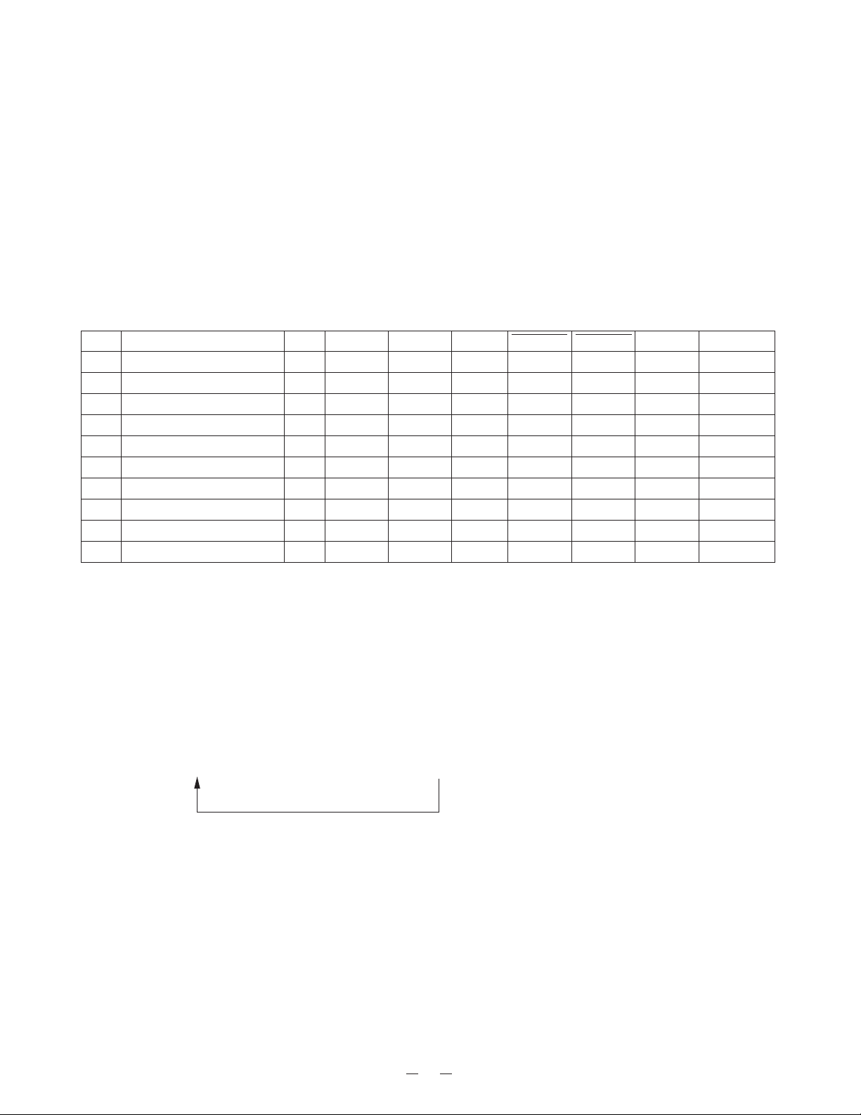
PRODUCT SAFETY NO TE : Products marked with a have special characteristics important to safety.
Before replacing any of these components, read carefully the product safety notice of this service manual.
Don’t degrade the safety of the product through important servicing.
Symbol F G J K M N Z P
% ± 1 ± 2 ± 5 ± 10 ± 20 ± 30 -20+80 0+100
LOC.
NO. NO.
CAPACITORS
The following codes indicate variation of capacitors against temper atures ,:
YA=±5%, YB=±10%, YD=+20-30%, YE=+20-50%(-25~+85°C), ZF=+30-80%,(-10~+79°C),
CH=0±60ppm/°C, TH=-470ppm/°C±60ppm/°C, B=±10%, F=+30-80%,
SL=+350ppm/°C~-1000ppm/°C, UJ=-750ppm/°C ±120ppm/°C , CJ=0±120ppm/°C , CK=0±250ppm/°C
C1 RC005216 BCMM813304Z CERAMIC M/L (1608) TAPE 33PF 50V J CH
C2 RC001807 BCAZ812296Z ELECTROLYTIC 2.2UF 50V M C-156
C3 RC005202 BCML311045Z CERAMIC M/L (1608) TAPE 0.1UF 16V K B
C4 RC005214 BCMM812214Z CERAMIC M/L (1608) TAPE 220PF 50V J CH
C5 RC005214 BCMM812214Z CERAMIC M/L (1608) TAPE 220PF 50V J CH
C6 RC005216 BCMM813304Z CERAMIC M/L (1608) TAPE 33PF 50V J CH
C7 RC005217 BCMM813314Z CERAMIC M/L (1608) TAPE 330PF 50V J CH
C8 RC005275 BCML813925Z CERAMIC M/L (1608) TAPE 0.0039UF 50V K B
C9 RC005202 BCML311045Z CERAMIC M/L (1608) TAPE 0.1UF 6V K B
C10 RC008271 BCMM813904Z CERAMIC M/L (1608) TAPE 39PF 50V J CH
C11 RC005205 BCML811035Z CERAMIC M/L (1608) TAPE 0.01UF 50V K B
C12 RC005219 BCMM814704Z CERAMIC M/L (1608) TAPE 47PF 50V J CH
C13 RC008472 BCEQ814786Z ELECTROLYTIC 0.47UF 50V M C-125
C14 RC001810 BCAZ814796Z ELECTROLYTIC 4.7UF 50V M C-156
C16 RC001807 BCAZ812296Z ELECTROLYTIC 2.2UF 50V M C-156
C17 RC001045 BCEQ311006Z ELECTROLYTIC 10UF 6V M C-125
C18 RC005204 BCML811025Z CERAMIC M/L (1608) TAPE 0.001UF 50V K B
C19 RC000777 BCZY0120001 SEMI-CONDUCT OR CZ-120 0.022UF 18V
C20 RC005204 BCML811025Z CERAMIC M/L (1608) TAPE 0.001UF 50V K B
C21 RC005205 BCML811035Z CERAMIC M/L (1608) TAPE 0.01UF 50V K B
C23 RC005212 BCMM811504Z CERAMIC M/L (1608) TAPE 15PF 50V J CH
C24 RC005205 BCML811035Z CERAMIC M/L (1608) TAPE 0.01UF 50V K B
C25 RC005223 BCMS812091Z CERAMIC M/L (1608) TAPE 2PF 50V C CK
C26 RC005210 BCMM811014Z CERAMIC M/L (1608) TAPE 100PF 50V J CH
C27 RC005202 BCML311045Z CERAMIC M/L (1608) TAPE 0.1UF 16V K B
C28 RC005202 BCML311045Z CERAMIC M/L (1608) TAPE 0.1UF 16V K B
C29 RC001810 BCAZ814796Z ELECTROLYTIC 4.7UF 50V M C-156
C30 RC005205 BCML811035Z CERAMIC M/L (1608) TAPE 0.01UF 50V K B
C31 RC005210 BCMM811014Z CERAMIC M/L (1608) TAPE 100PF 50V J CH
C32 RC005202 BCML311045Z CERAMIC M/L (1608) TAPE 0.1UF 16V K B
C33 RC005206 BCML812225Z CERAMIC M/L (1608) TAPE 0.0022UF 50V K B
C34 RC005207 BCML813325Z CERAMIC M/L (1608) TAPE 0.0033UF 50V K B
PART NO.
REF.
DESCRIPTION
Symbol C D
pF ± 0.25 ± 0.5
44
Page 42

LOC.
NO. NO.
C35 RC005202 BCML311045Z CERAMIC M/L (1608) TAPE 0.1UF 16V K B
C36 RC008318 BCML815625Z CERAMIC M/L (1608) TAPE 0.0056UF 50V K B
C37 RC005276 BCML818225Z CERAMIC M/L (1608) TAPE 0.0082UF 50V K B
C38 RC001809 BCAZ814786Z ELECTROLYTIC 0.47UF 50V M C-156
C39 RC005206 BCML812225Z CERAMIC M/L (1608) TAPE 0.0022UF 50V K B
C40 RC005202 BCML311045Z CERAMIC M/L (1608) TAPE 0.1UF 16V K B
C41 RC005181 BCEQ811096Z ELECTROLYTIC 1UF 50V M C-125
C42 RC005467 BCEQ114706Z ELECTROLYTIC 47UF 10V M C-125
C43 RC005202 BCML311045Z CERAMIC M/L (1608) TAPE 0.1UF 16V K B
C44 RC005202 BCML311045Z CERAMIC M/L (1608) TAPE 0.1UF 16V K B
C45 RC005202 BCML311045Z CERAMIC M/L (1608) TAPE 0.1UF 16V K B
C46 RC005202 BCML311045Z CERAMIC M/L (1608) TAPE 0.1UF 16V K B
C47 RC005203 BCML512235Z CERAMIC M/L (1608) TAPE 0.022UF 25V K B
C48 RC001794 BCAZ111016Z ELECTROLYTIC 100UF 10V M C-156
C49 RC000752 BCKB821025Z CERAMIC 0.001UF 500V K YB(B)
C50 RC005204 BCML811025Z CERAMIC M/L (1608) TAPE 0.001UF 50V K B
C51 RC008111 BCZY0259001 MYLAR METALLIZED CZ-259 1UF 250V
C52 RC005210 BCMM811014Z CERAMIC M/L (1608) TAPE 100PF 50V J CH
C53 RC005210 BCMM811014Z CERAMIC M/L (1608) TAPE 100PF 50V J CH
C54 RC005360 BCMM816092Z CERAMIC M/L (1608) TAPE 6PF 50V D CH
C55 RC005210 BCMM811014Z CERAMIC M/L (1608) TAPE 100PF 50V J CH
C57 RC005204 BCML811025Z CERAMIC M/L (1608) TAPE 0.001UF 50V K B
C59 RC005205 BCML811035Z CERAMIC M/L (1608) TAPE 0.01UF 50V K B
C60 RC008146 BCML816825Z CERAMIC M/L (1608) TAPE 0.0068UF 50V K B
C61 RC001802 BCAZ314706Z ELECTROLYTIC 47UF 16V M C-156
C62 RC001802 BCAZ314706Z ELECTROLYTIC 47UF 16V M C-156
C64 RC001805 BCAZ811096Z ELECTROLYTIC 1UF 50V M C-156
C65 RC005204 BCML811025Z CERAMIC M/L (1608) TAPE 0.001UF 50V K B
C66 RC005210 BCMM811014Z CERAMIC M/L (1608) TAPE 100PF 50V J CH
C67 RC005204 BCML811025Z CERAMIC M/L (1608) TAPE 0.001UF 50V K B
C68 RC004167 BCAZ511016Z ELECTROLYTIC 100UF 25V M C-156
C69 RC005205 BCML811035Z CERAMIC M/L (1608) TAPE 0.01UF 50V K B
C73 RC005206 BCML812225Z CERAMIC M/L (1608) TAPE 0.0022UF 50V K B
C74 RC005215 BCMM812704Z CERAMIC M/L (1608) TAPE 27PF 50V J CH
C75 RC005215 BCMM812704Z CERAMIC M/L (1608) TAPE 27PF 50V J CH
C76 RC005203 BCML512235Z CERAMIC M/L (1608) TAPE 0.022UF 25V K B
C77 RC005420 BCMM811514Z CERAMIC M/L (1608) TAPE 150PF 50V J CH
C78 RC001794 BCAZ111016Z ELECTROLYTIC 100UF 10V M C-156
C79 RC004445 BCAZ903316Z ELECTROLYTIC 330UF 6.3V M C-156
C80 RC004445 BCAZ903316Z ELECTROLYTIC 330UF 6.3V M C-156
C81 RC008731 BCXK311050Z CERAMIC M/L (2125) TAPE 1UF 16V Z F
C82 RC005205 BCML811035Z CERAMIC M/L (1608) TAPE 0.01UF 50V K B
C83 RC008473 BCMF511040Z CERAMIC M/L (1608) TAPE 0.1UF 25V Z F
C84 RC008731 BCXK311050Z CERAMIC M/L (2125) TAPE 1UF 16V Z F
C85 RC005322 BCAZ312226Z ELECTROLYTIC 2200UF 16V M C-156
C86 RC002229 BCXT511045Z CERAMIC M/L (2125) TAPE 0.1UF 25V K B
C87 RC005204 BCML811025Z CERAMIC M/L (1608) TAPE 0.001UF 50V K B
PART NO.
REF.
DESCRIPTION
45
Page 43

LOC.
NO. NO.
C88 RC005205 BCML811035Z CERAMIC M/L (1608) TAPE 0.01UF 50V K B
C89 RC008106 BCAZ313316Z ELECTROLYTIC 330UF 16V M C-156
C90 RC005205 BCML811035Z CERAMIC M/L (1608) TAPE 0.01UF 50V K B
C91 RC001794 BCAZ111016Z ELECTROLYTIC 100UF 10V M C-156
C92 RC001794 BCAZ111016Z ELECTROLYTIC 100UF 10V M C-156
C93 RC005468 BCEQ904706Z ELECTROLYTIC 47UF 6.3V M C-125
C94 RC008731 BCXK311050Z CERAMIC M/L (2125) TAPE 1UF 16V Z F
C95 RC005202 BCML311045Z CERAMIC M/L (1608) TAPE 0.1UF 16V K B
C96 RC005276 BCML818225Z CERAMIC M/L (1608) TAPE 0.0082UF 50V K B
C97 RC008731 BCXK311050Z CERAMIC M/L (2125) TAPE 1UF 16V Z F
C98 RC008731 BCXK311050Z CERAMIC M/L (2125) TAPE 1UF 16V Z F
C99 RC005204 BCML811025Z CERAMIC M/L (1608) TAPE 0.001UF 50V K B
C100 RC004445 BCAZ903316Z ELECTROLYTIC 330UF 6.3V M C-156
C103 RC008473 BCMF511040Z CERAMIC M/L (1608) TAPE 0.1UF 25V Z F
C104 RC001794 BCAZ111016Z ELECTROLYTIC 100UF 10V M C-156
C105 RC001794 BCAZ111016Z ELECTROLYTIC 100UF 10V M C-156
C106 RC005204 BCML811025Z CERAMIC M/L (1608) TAPE 0.001UF 50V K B
C107 RC005202 BCML311045Z CERAMIC M/L (1608) TAPE 0.1UF 16V K B
C108 RC002850 BCXS811025Z CERAMIC M/L (3216) TAPE 0.001UF 50V K B
C109 RC008731 BCXK311050Z CERAMIC M/L (2125) TAPE 1UF 16V Z F
C114 RC008473 BCMF511040Z CERAMIC M/L (1608) TAPE 0.1UF 25V Z F
C115 RC005205 BCML811035Z CERAMIC M/L (1608) TAPE 0.01UF 50V K B
C116 RC008473 BCMF511040Z CERAMIC M/L (1608) TAPE 0.1UF 25V Z F
C117 RC005218 BCMM814091Z CERAMIC M/L (1608) TAPE 4PF 50V C CH
C118 RC005635 BCKB134715Z CERAMIC 470PF 1000V K YB(B)
C119 RC005635 BCKB134715Z CERAMIC 470PF 1000V K YB(B)
C120 RC001794 BCAZ111016Z ELECTROLYTIC 100UF 10V M C-156
C121 RC005322 BCAZ312226Z ELECTROLYTIC 2200UF 16V M C-156
C122 RC008731 BCXK311050Z CERAMIC M/L (2125) TAPE 1UF 16V Z F
C123 RC005202 BCML311045Z CERAMIC M/L (1608) TAPE 0.1UF 16V K B
C124 RC005216 BCMM813304Z CERAMIC M/L (1608) TAPE 33PF 50V J CH
C125 RC001045 BCEQ311006Z ELECTROLYTIC 10UF 16V M C-125
C126 RC005204 BCML811025Z CERAMIC M/L (1608) TAPE 0.001UF 50V K B
C127 RC005204 BCML811025Z CERAMIC M/L (1608) TAPE 0.001UF 50V K B
C129 RC005202 BCML311045Z CERAMIC M/L (1608) TAPE 0.1UF 16V K B
C130 RC005205 BCML811035Z CERAMIC M/L (1608) TAPE 0.01UF 50V K B
C203 RC001811 BCAZ901016Z ELECTROLYTIC 100UF 6.3V M C-156
C205 RC008146 BCML816825Z CERAMIC M/L (1608) TAPE 0.0068UF 50V K B
C206 RC008296 BCSH901006Z TANTALUM CHIP TAPE 10UF 6.3V M C-122
C207 RC008296 BCSH901006Z TANTALUM CHIP TAPE 10UF 6.3V M C-122
C208 RC005219 BCMM814704Z CERAMIC M/L (1608) TAPE 47PF 50V J CH
C209 RC008485 BCMM813914Z CERAMIC M/L (1608) TAPE 390PF 50V J CH
C210 RC005202 BCML311045Z CERAMIC M/L (1608) TAPE 0.1UF 16V K B
C211 RC008296 BCSH901006Z TANTALUM CHIP TAPE 10UF 6.3V M C-122
C213 RC005202 BCML311045Z CERAMIC M/L (1608) TAPE 0.1UF 16V K B
C214 RC005202 BCML311045Z CERAMIC M/L (1608) TAPE 0.1UF 16V K B
C215 RC005207 BCML813325Z CERAMIC M/L (1608) TAPE 0.0033UF 50V K B
PART NO.
REF.
DESCRIPTION
46
Page 44

LOC.
NO. NO.
C216 RC008926 BCMM518214Z CERAMIC M/L (1608) TAPE 820PF 25V J CH
C217 RC008270 BCML811235Z CERAMIC M/L (1608) TAPE 0.012UF 50V K B
C218 RC005204 BCML811025Z CERAMIC M/L (1608) TAPE 0.001UF 50V K B
C219 RC005204 BCML811025Z CERAMIC M/L (1608) TAPE 0.001UF 50V K B
C220 RC005206 BCML812225Z CERAMIC M/L (1608) TAPE 0.0022UF 50V K B
C221 RC005202 BCML311045Z CERAMIC M/L (1608) TAPE 0.1UF 16V K B
C222 RC008296 BCSH901006Z TANTALUM CHIP TAPE 10UF 6.3V M C-122
C223 RC005204 BCML811025Z CERAMIC M/L (1608) TAPE 0.001UF 50V K B
C224 RC005204 BCML811025Z CERAMIC M/L (1608) TAPE 0.001UF 50V K B
C225 RC005202 BCML311045Z CERAMIC M/L (1608) TAPE 0.1UF 16V K B
C226 RC008296 BCSH901006Z TANTALUM CHIP TAPE 10UF 6.3V M C-122
C227 RC005204 BCML811025Z CERAMIC M/L (1608) TAPE 0.001UF 50V K B
C228 RC005202 BCML311045Z CERAMIC M/L (1608) TAPE 0.1UF 16V K B
C230 RC005202 BCML311045Z CERAMIC M/L (1608) TAPE 0.1UF 16V K B
C231 RC005202 BCML311045Z CERAMIC M/L (1608) TAPE 0.1UF 16V K B
C232 RC005209 BCMM811002Z CERAMIC M/L (1608) TAPE 10PF 50V D CH
C233 RC005209 BCMM811002Z CERAMIC M/L (1608) TAPE 10PF 50V D CH
C234 RC005202 BCML311045Z CERAMIC M/L (1608) TAPE 0.1UF 16V K B
C235 RC005205 BCML811035Z CERAMIC M/L (1608) TAPE 0.01UF 50V K B
C236 RC005205 BCML811035Z CERAMIC M/L (1608) TAPE 0.01UF 50V K B
C237 RC005205 BCML811035Z CERAMIC M/L (1608) TAPE 0.01UF 50V K B
C238 RC005205 BCML811035Z CERAMIC M/L (1608) TAPE 0.01UF 50V K B
C239 RC005204 BCML811025Z CERAMIC M/L (1608) TAPE 0.001UF 50V K B
C240 RC005202 BCML311045Z CERAMIC M/L (1608) TAPE 0.1UF 16V K B
C241 RC005202 BCML311045Z CERAMIC M/L (1608) TAPE 0.1UF 16V K B
C242 RC005202 BCML311045Z CERAMIC M/L (1608) TAPE 0.1UF 16V K B
C244 RC005203 BCML512235Z CERAMIC M/L (1608) TAPE 0.022UF 25V K B
C245 RC008926 BCMM518214Z CERAMIC M/L (1608) TAPE 820PF 25V J CH
C246 RC005204 BCML811025Z CERAMIC M/L (1608) TAPE 0.001UF 50V K B
C247 RC005274 BCML811535Z CERAMIC M/L (1608) TAPE 0.015UF 50V K B
C248 RC005274 BCML811535Z CERAMIC M/L (1608) TAPE 0.015UF 50V K B
C249 RC005208 BCML814725Z CERAMIC M/L (1608) TAPE 0.0047UF 50V K B
C250 RC005202 BCML311045Z CERAMIC M/L (1608) TAPE 0.1UF 16V K B
C251 RC005202 BCML311045Z CERAMIC M/L (1608) TAPE 0.1UF 16V K B
C252 RC008884 BCAZ904716Z ELECTROLYTIC 470UF 6.3V M C-156
C253 RC005202 BCML311045Z CERAMIC M/L (1608) TAPE 0.1UF 16V K B
C401 RC005216 BCMM813304Z CERAMIC M/L (1608) TAPE 33PF 50V J CH
C402 RC005401 BCXT111055Z CERAMIC M/L (2125) TAPE 1UF 10V K B
C403 RC005202 BCML311045Z CERAMIC M/L (1608) TAPE 0.1UF 16V K B
C404 RC005214 BCMM812214Z CERAMIC M/L (1608) TAPE 220PF 50V J CH
C405 RC005214 BCMM812214Z CERAMIC M/L (1608) TAPE 220PF 50V J CH
C406 RC005216 BCMM813304Z CERAMIC M/L (1608) TAPE 33PF 50V J CH
C407 RC005217 BCMM813314Z CERAMIC M/L (1608) TAPE 330PF 50V J CH
C408 RC005207 BCML813325Z CERAMIC M/L (1608) TAPE 0.0033UF 50V K B
C409 RC005202 BCML311045Z CERAMIC M/L (1608) TAPE 0.1UF 16V K B
C410 RC005203 BCML512235Z CERAMIC M/L (1608) TAPE 0.022UF 25V K B
C414 RC005202 BCML311045Z CERAMIC M/L (1608) TAPE 0.1UF 16V K B
PART NO.
REF.
DESCRIPTION
47
Page 45

LOC.
NO. NO.
C416 RC002594 BCXT516835Z CERAMIC M/L (2125) TAPE 0.068UF 25V K B
C417 RC004347 BCXK514740Z CERAMIC M/L (2125) TAPE 0.47UF 25V Z F
C418 RC002229 BCXT511045Z CERAMIC M/L (2125) TAPE 0.1UF 25V K B
C419 RC008318 BCML815625Z CERAMIC M/L (1608) TAPE 0.0056UF 50V K B
C421 RC005216 BCMM813304Z CERAMIC M/L (1608) TAPE 33PF 50V J CH
C422 RC005209 BCMM811002Z CERAMIC M/L (1608) TAPE 10PF 50V D CH
C423 RC005205 BCML811035Z CERAMIC M/L (1608) TAPE 0.01UF 50V K B
C424 RC005202 BCML311045Z CERAMIC M/L (1608) TAPE 0.1UF 16V K B
C425 RC005224 BCMT813091Z CERAMIC M/L (1608) TAPE 3PF 50V C CJ
C426 RC005205 BCML811035Z CERAMIC M/L (1608) TAPE 0.01UF 50V K B
C427 RC005211 BCMM811204Z CERAMIC M/L (1608) TAPE 12PF 50V J CH
C428 RC005210 BCMM811014Z CERAMIC M/L (1608) TAPE 100PF 50V J CH
C430 RC005210 BCMM811014Z CERAMIC M/L (1608) TAPE 100PF 50V J CH
C431 RC008268 BCML314735Z CERAMIC M/L (1608) TAPE 0.047UF 16V K B
C432 RC008319 BCSH904796Z TANTALUM CHIP TAPE 4.7UF 6.3V M C-122
C433 RC008268 BCML314735Z CERAMIC M/L (1608) TAPE 0.047UF 16V K B
C434 RC005205 BCML811035Z CERAMIC M/L (1608) TAPE 0.01UF 50V K B
C435 RC005202 BCML311045Z CERAMIC M/L (1608) TAPE 0.1UF 16V K B
C437 RC005206 BCML812225Z CERAMIC M/L (1608) TAPE 0.0022UF 50V K B
C438 RC008319 BCSH904796Z TANTALUM CHIP TAPE 4.7UF 6.3V M C-122
C439 RC008319 BCSH904796Z TANTALUM CHIP TAPE 4.7UF 6.3V M C-122
C440 RC004449 BCXT311545Z CERAMIC M/L (2125) TAPE 0.15UF 16V K B
C441 RC005202 BCML311045Z CERAMIC M/L (1608) TAPE 0.1UF 16V K B
C442 RC005276 BCML818225Z CERAMIC M/L (1608) TAPE 0.0082UF 50V K B
C443 RC004347 BCXK514740Z CERAMIC M/L (2125) TAPE 0.47UF 25V Z F
C444 RC008319 BCSH904796Z TANTALUM CHIP TAPE 4.7UF 6.3V M C-122
C445 RC004347 BCXK514740Z CERAMIC M/L (2125) TAPE 0.47UF 25V Z F
C446 RC005205 BCML811035Z CERAMIC M/L (1608) TAPE 0.01UF 50V K B
C447 RC004412 BCXT312245Z CERAMIC M/L (2125) TAPE 0.22UF 16V K B
C448 RC005275 BCML813925Z CERAMIC M/L (1608) TAPE 0.0039UF 50V K B
C449 RC005205 BCML811035Z CERAMIC M/L (1608) TAPE 0.01UF 50V K B
C450 RC008268 BCML314735Z CERAMIC M/L (1608) TAPE 0.047UF 16V K B
C451 RC004657 BCEQ514796Z ELECTROLYTIC 4.7UF 25V M C-125
C452 RC005224 BCMT813091Z CERAMIC M/L (1608) TAPE 3PF 50V C CJ
C453 RC005275 BCML813925Z CERAMIC M/L (1608) TAPE 0.0039UF 50V K B
C454 RC005202 BCML311045Z CERAMIC M/L (1608) TAPE 0.1UF 16V K B
C455 RC005208 BCML814725Z CERAMIC M/L (1608) TAPE 0.0047UF 50V K B
C456 RC001045 BCEQ311006Z ELECTROLYTIC 10UF 16V M C-125
C457 RC005208 BCML814725Z CERAMIC M/L (1608) TAPE 0.0047UF 50V K B
C458 RC005222 BCMS811091Z CERAMIC M/L (1608) TAPE 1PF 50V C CK
C459 RC005216 BCMM813304Z CERAMIC M/L (1608) TAPE 33PF 50V J CH
C460 RC005216 BCMM813304Z CERAMIC M/L (1608) TAPE 33PF 50V J CH
C461 RC003284 BCFZ901016Z ELECTROLYTIC 100UF 6.3V M C-258
C462 RC005205 BCML811035Z CERAMIC M/L (1608) TAPE 0.01UF 50V K B
C463 RC005205 BCML811035Z CERAMIC M/L (1608) TAPE 0.01UF 50V K B
C464 RC008731 BCXK311050Z CERAMIC M/L (2125) TAPE 1UF 16V Z F
C465 RC005207 BCML813325Z CERAMIC M/L (1608) TAPE 0.0033UF 50V K B
PART NO.
REF.
DESCRIPTION
48
Page 46

LOC.
NO. NO.
C466 RC005207 BCML813325Z CERAMIC M/L (1608) TAPE 0.0033UF 50V K B
C467 RC003284 BCFZ901016Z ELECTROLYTIC 100UF 6.3V M C-258
C468 RC005205 BCML811035Z CERAMIC M/L (1608) TAPE 0.01UF 50V K B
C469 RC008296 BCSH901006Z TANTALUM CHIP TAPE 10UF 6.3V M C-122
C470 RC005203 BCML512235Z CERAMIC M/L (1608) TAPE 0.022UF 25V K B
C471 RC005205 BCML811035Z CERAMIC M/L (1608) TAPE 0.01UF 50V K B
C472 RC005205 BCML811035Z CERAMIC M/L (1608) TAPE 0.01UF 50V K B
C473 RC005202 BCML311045Z CERAMIC M/L (1608) TAPE 0.1UF 16V K B
C474 RC008296 BCSH901006Z TANTALUM CHIP TAPE 10UF 6.3V M C-122
CT001 RC008272 BCTY0076100 TRIMMER CT-076 TZ3Z100FR 10PF
CT401 RC008272 BCTY0076100 TRIMMER CT-076 TZ3Z100FR 10PF
DIODES
D1 RC002236 BDA Y0246003 AX TS 26+ 1N4148 T-77
D2 RC002236 BDA Y0246003 AX TS 26+ 1N4148 T-77
D3 RC002470 BDAY0492033 ZENER AX TS 26 + HZ7C3 TD
D4 RC001826 BDA Y0433001 RLS4148 TE11
D5 RC002236 BDA Y0246003 AX TS 26+ 1N4148 T-77
D6 RC002236 BDA Y0246003 AX TS 26+ 1N4148 T-77
D7 RC003194 BDA Y0272010 ZENER HZ33CP
D8 RC002236 BDA Y0246003 AX TS 26+ 1N4148 T-77
D9 RC002236 BDA Y0246003 AX TS 26+ 1N4148 T-77
D10 RC002236 BDA Y0246003 AX TS 26+ 1N4148 T -77
D11 RC002236 BDA Y0246003 AX TS 26+ 1N4148 T -77
D14 RC008273 BDAY0492036 ZENER AX TS 26 + HZ4B1 TD
D15 RC003195 BDA Y0432004 ZENER HZK6C TR
D16 RC002236 BDA Y0246003 AX TS 26+ 1N4148 T -77
D18 RC003196 BDAY0492025 ZENER AX TS 26 + HZ7A1 TD
D25 RC002236 BDA Y0246003 AX TS 26+ 1N4148 T -77
D26 RC002236 BDA Y0246003 AX TS 26+ 1N4148 T -77
D28 RC002236 BDA Y0246003 AX TS 26+ 1N4148 T -77
D29 RC002236 BDA Y0246003 AX TS 26+ 1N4148 T -77
D30 RC002236 BDA Y0246003 AX TS 26+ 1N4148 T -77
D31 RC008474 BDAY0492038 ZENER AX TS 26 + HZ4C3 TD
D201 RC008320 BD AY1092001 LED SML-310L T T86
D202 RC008407 BD A Y1060001 LED SML-310MT T86
D203 RC008486 BD A Y1091001 ZENER NNCD6.2F-T1B
D205 RC005412 BD A Y0825001 LED LTD-482P-03
D206 RC008407 BD A Y1060001 LED SML-310MT T86
D207 RC001826 BD A Y0433001 RLS4148 TE11
D208 RC008320 BD AY1092001 LED SML-310L T T86
D209 RC001826 BD A Y0433001 RLS4148 TE11
D213 RC001826 BD A Y0433001 RLS4148 TE11
D214 RC003195 BD A Y0432004 ZENER HZK6C TR
D217 RC001826 BD A Y0433001 RLS4148 TE11
D218 RC001826 BD A Y0433001 RLS4148 TE11
D401 RC001826 BD A Y0433001 RLS4148 TE11
D402 RC001826 BD A Y0433001 RLS4148 TE11
PART NO.
REF.
DESCRIPTION
49
Page 47

LOC.
NO. NO.
D403 RC003195 BD A Y0432004 ZENER HZK6C TR
D404 RC003195 BD A Y0432004 ZENER HZK6C TR
D405 RC001826 BD A Y0433001 RLS4148 TE11
D406 RC001826 BD A Y0433001 RLS4148 TE11
D407 RC002240 BD A Y0485001 HSM88WA TL
D408 RC008320 BD AY1092001 LED SML-310L T T86
FIL TERS
FT1 RC008279 BFLY0971001 CERAMIC FL-971 FFE1054NA11UXL
FT2 RC008280 BFLY0977001 FL-977 LTFS455B5
FT401 RC008279 BFLY0971001 CERAMIC FL-971 FFE1054NA11UXL
FT402 RC008280 BFLY0977001 FL-977 L TFS455B5
IC’s
IC1 RC008278 BDEY3870003 LA8633VU-TLM
IC2 RC001640 BDEY1146001 PC817CD
IC3 RC004870 BDEY2768003 MC3361CDR2
IC4 RC004045 BDEY0861002 M5223FP-600C T APE
IC5 RC001640 BDEY1146001 PC817CD
IC7 RC005075 BDEY2938003 RH5VL40CA-T1
IC11 RC008475 BDD Y0889001 UC2348 MB89173PF-G-233-BND-U
IC201 RC005423 BDEY1533003 MC34119D R2
IC202 RC008487 BDD Y0992001 UC2369A SEL D16559UAA11EQC-3V
IC204 RC008488 BDEY1749003 TC74HC00AF(EL)
IC207 RC004595 BDEY2486003 RH5VL45AA-T1
IC208 RC008489 BDEY3868001 KM29W040AT
IC401 RC004870 BDEY2768003 MC3361CDR2
IC403 RC008278 BDEY3870003 LA8633VU-TLM
IC404 RC008505 BDD Y0890001 UC2349 MB89174LPF-G-234-BND-U
IC405 RC008322 BDEY3882003 TK11130SCL
IC406 RC008323 BDEY3886003 XC612N3328MR
JACKS
J1 RC003586 BJKY0803002 TEL JK-803 A36-006-4910A 2P
J4 RC001094 BJKY0234001 JK-234 DJ13-1
J6 RC005650 BJKY0944020 JK-944 IMSA-9604S-20C 20P
J11 RC002252 BJKY0600002 JK-600 SB20-02WS 2P
J202 RC005649 BJKY0943020 JK-943 9604S-20F 20P
J401 RC001653 BJKY0571001 JK-571 M60-002-020-HKAD
COILS
L2 RC008282 BLZY0136399 INDUCTOR:MOLDED CHIP LZ136 MLF1608A3R9KT 3.9UH
L3 RC004073 BLZY0051479 INDUCTOR:MOLDED LZ-051 SP0305-4R7K2 4.7UH
L4 RC008281 BLBY1175001 LB-1175 7002BE-A0026HM
L5 RC004073 BLZY0051479 INDUCTOR:MOLDED LZ-051 SP0305-4R7K2 4.7UH
L6 RC008451 BLZY0181826 INDUCTOR:MOLDED CHIP TAPE LZ-181 8.2NH
L201 RC008490 BLZY0203102 INDUCTOR:MOLDED CHIP LZ-203 MMZ1608R102AT 1000
L401 RC008397 BLZY0136100 INDUCTOR:MOLDED CHIP LZ-136 MLF1608K100KT 10UH
L402 RC008281 BLBY1175001 LB-1175 7002BE-A0026HM
L403 RC008283 BLZY0181127 INDUCTOR:MOLDED CHIP TAPE LZ-181 12NH J
T1 RC003234 BTFY0265001 TRANSFORMER:HYBRID TF-265 AT-24E7-1B/R295403
PART NO.
REF.
DESCRIPTION
50
Page 48

LOC.
NO. NO.
TRANSISTORS
Q1 RC002245 BDBC2714124 DB-718 2SC2714-Y TE85L
Q2 RC003031 BDBC1623648 DB-380 2SC1623-L6 T1B
Q3 RC003031 BDBC1623648 DB-380 2SC1623-L6 T1B
Q4 RC003031 BDBC1623648 DB-380 2SC1623-L6 T1B
Q5 RC008275 BDBA0812695 DB-035 2SA812(M)-M6A T1B
Q6 RC008275 BDBA0812695 DB-035 2SA812(M)-M6A T1B
Q7 RC003031 BDBC1623648 DB-380 2SC1623-L6 T1B
Q8 RC003200 BDBD0471111 DB-411 2SD471-L
Q9 RC003031 BDBC1623648 DB-380 2SC1623-L6 T1B
Q10 RC003031 BDBC1623648 DB-380 2SC1623-L6 T1B
Q11 RC000799 BDBC2120124 DB-300 2SC2120-Y
Q12 RC003200 BDBD0471111 DB-411 2SD471-L
Q13 RC003031 BDBC1623648 DB-380 2SC1623-L6 T1B
Q14 RC003200 BDBD0471111 DB-411 2SD471-L
Q17 RC003031 BDBC1623648 DB-380 2SC1623-L6 T1B
Q18 RC003200 BDBD0471111 DB-411 2SD471-L
Q19 RC003031 BDBC1623648 DB-380 2SC1623-L6 T1B
Q20 RC003031 BDBC1623648 DB-380 2SC1623-L6 T1B
Q21 RC003031 BDBC1623648 DB-380 2SC1623-L6 T1B
Q22 RC003031 BDBC1623648 DB-380 2SC1623-L6 T1B
Q201 RC003031 BDBC1623648 DB-380 2SC1623-L6 T1B
Q202 RC003031 BDBC1623648 DB-380 2SC1623-L6 T1B
Q401 RC002245 BDBC2714124 DB-718 2SC2714-Y TE85L
Q402 RC003031 BDBC1623648 DB-380 2SC1623-L6 T1B
Q403 RC008275 BDBA0812695 DB-035 2SA812(M)-M6A T1B
Q404 RC003031 BDBC1623648 DB-380 2SC1623-L6 T1B
Q405 RC003031 BDBC1623648 DB-380 2SC1623-L6 T1B
Q406 RC003031 BDBC1623648 DB-380 2SC1623-L6 T1B
Q407 RC003031 BDBC1623648 DB-380 2SC1623-L6 T1B
Q408 RC003031 BDBC1623648 DB-380 2SC1623-L6 T1B
Q409 RC003031 BDBC1623648 DB-380 2SC1623-L6 T1B
Q410 RC003031 BDBC1623648 DB-380 2SC1623-L6 T1B
Q411 RC003031 BDBC1623648 DB-380 2SC1623-L6 T1B
Q412 RC003031 BDBC1623648 DB-380 2SC1623-L6 T1B
RESISTORS
R1 RC005249 BRFC162244Z CARBON FIXED CHIP 220K 1/16W J TAPING
R2 RC005259 BRFC166814Z CARBON FIXED CHIP 680 1/16W J TAPING
R3 RC005255 BRFC164714Z CARBON FIXED CHIP 470 1/16W J TAPING
R4 RC005245 BRFC161834Z CARBON FIXED CHIP 18K 1/16W J TAPING
R5 RC005281 BRFC162224Z CARBON FIXED CHIP 2.2K 1/16W J TAPING
R6 RC005258 BRFC164744Z CARBON FIXED CHIP 470K 1/16W J TAPING
R8 RC005241 BRFC161034Z CARBON FIXED CHIP 10K 1/16W J TAPING
R9 RC005253 BRFC163324Z CARBON FIXED CHIP 3.3K 1/16W J TAPING
R11 RC005258 BRFC164744Z CARBON FIXED CHIP 470K 1/16W J TAPING
R12 RC005282 BRFC162714Z CARBON FIXED CHIP 270 1/16W J TAPING
R13 RC005281 BRFC162224Z CARBON FIXED CHIP 2.2K 1/16W J TAPING
PART NO.
REF.
DESCRIPTION
51
Page 49

LOC.
NO. NO.
R14 RC005241 BRFC161034Z CARBON FIXED CHIP 10K 1/16W J TAPING
R16 RC008029 BRFC163924Z CARBON FIXED CHIP 3.9K 1/16W J TAPING
R17 RC005280 BRFC161534Z CARBON FIXED CHIP 15K 1/16W J TAPING
R18 RC005260 BRFC166834Z CARBON FIXED CHIP 68K 1/16W J TAPING
R19 RC005286 BRFC165644Z CARBON FIXED CHIP 560K 1/16W J TAPING
R20 RC005242 BRFC161044Z CARBON FIXED CHIP 100K 1/16W J TAPING
R21 RC005260 BRFC166834Z CARBON FIXED CHIP 68K 1/16W J TAPING
R22 RC005259 BRFC166814Z CARBON FIXED CHIP 680 1/16W J TAPING
R23 RC005281 BRFC162224Z CARBON FIXED CHIP 2.2K 1/16W J TAPING
R24 RC002350 BRSN101514Z METAL OXIDE(FORMED) 150 1W J (P=12.5)
R25 RC005311 BRFC160004Z CARBON FIXED CHIP 0 1/16W J TAPING
R26 RC005241 BRFC161034Z CARBON FIXED CHIP 10K 1/16W J TAPING
R27 RC005245 BRFC161834Z CARBON FIXED CHIP 18K 1/16W J TAPING
R28 RC005242 BRFC161044Z CARBON FIXED CHIP 100K 1/16W J TAPING
R29 RC002899 BRFC180004Z CARBON FIXED CHIP 0 1/8W J TAPING
R30 RC005242 BRFC161044Z CARBON FIXED CHIP 100K 1/16W J TAPING
R32 RC005248 BRFC162234Z CARBON FIXED CHIP 22K 1/16W J TAPING
R33 RC005248 BRFC162234Z CARBON FIXED CHIP 22K 1/16W J TAPING
R34 RC005242 BRFC161044Z CARBON FIXED CHIP 100K 1/16W J TAPING
R35 RC008286 BRFC162744Z CARBON FIXED CHIP 270K 1/16W J TAPING
R36 RC008482 BRFC186804Z CARBON FIXED CHIP 68 1/8W J TAPING
R37 RC008091 BRFC165614Z CARBON FIXED CHIP 560 1/16W J TAPING
R38 RC005259 BRFC166814Z CARBON FIXED CHIP 680 1/16W J TAPING
R39 RC005257 BRFC164734Z CARBON FIXED CHIP 47K 1/16W J TAPING
R40 RC008030 BRFC165624Z CARBON FIXED CHIP 5.6K 1/16W J TAPING
R41 RC005261 BRFC168224Z CARBON FIXED CHIP 8.2K 1/16W J TAPING
R42 RC005239 BRFC161014Z CARBON FIXED CHIP 100 1/16W J TAPING
R43 RC002335 BRFC183314Z CARBON FIXED CHIP 330 1/8W J TAPING
R44 RC003231 BRSJ222234Z METAL OXIDE 22K 1/2WS J
R45 RC005256 BRFC164724Z CARBON FIXED CHIP 4.7K 1/16W J TAPING
R46 RC005242 BRFC161044Z CARBON FIXED CHIP 100K 1/16W J TAPING
R47 RC005242 BRFC161044Z CARBON FIXED CHIP 100K 1/16W J TAPING
R48 RC005278 BRFC161244Z CARBON FIXED CHIP 120K 1/16W J TAPING
R49 RC005432 BRFC161544Z CARBON FIXED CHIP 150K 1/16W J TAPING
R50 RC005240 BRFC161024Z CARBON FIXED CHIP 1K 1/16W J TAPING
R51 RC005240 BRFC161024Z CARBON FIXED CHIP 1K 1/16W J TAPING
R52 RC005240 BRFC161024Z CARBON FIXED CHIP 1K 1/16W J TAPING
R53 RC005240 BRFC161024Z CARBON FIXED CHIP 1K 1/16W J TAPING
R54 RC005257 BRFC164734Z CARBON FIXED CHIP 47K 1/16W J TAPING
R55 RC008029 BRFC163924Z CARBON FIXED CHIP 3.9K 1/16W J TAPING
R56 RC005241 BRFC161034Z CARBON FIXED CHIP 10K 1/16W J TAPING
R57 RC005249 BRFC162244Z CARBON FIXED CHIP 220K 1/16W J TAPING
R58 RC005258 BRFC164744Z CARBON FIXED CHIP 470K 1/16W J TAPING
R59 RC005242 BRFC161044Z CARBON FIXED CHIP 100K 1/16W J TAPING
R60 RC005260 BRFC166834Z CARBON FIXED CHIP 68K 1/16W J TAPING
R62 RC005257 BRFC164734Z CARBON FIXED CHIP 47K 1/16W J TAPING
R63 RC008767 BRFC163344Z CARBON FIXED CHIP 330K 1/16W J TAPING
PART NO.
REF.
DESCRIPTION
52
Page 50

LOC.
NO. NO.
R64 RC008734 BRFC162254Z CARBON FIXED CHIP 2.2M 1/16W J TAPING
R65 RC005241 BRFC161034Z CARBON FIXED CHIP 10K 1/16W J TAPING
R66 RC004183 BRSJ001024Z METAL OXIDE 1K 1WS J
R67 RC005280 BRFC161534Z CARBON FIXED CHIP 15K 1/16W J TAPING
R68 RC005280 BRFC161534Z CARBON FIXED CHIP 15K 1/16W J TAPING
R69 RC005280 BRFC161534Z CARBON FIXED CHIP 15K 1/16W J TAPING
R70 RC001790 BRFC181534Z CARBON FIXED CHIP 15K 1/8W J TAPING
R71 RC005256 BRFC164724Z CARBON FIXED CHIP 4.7K 1/16W J TAPING
R72 RC005256 BRFC164724Z CARBON FIXED CHIP 4.7K 1/16W J TAPING
R73 RC005240 BRFC161024Z CARBON FIXED CHIP 1K 1/16W J TAPING
R74 RC005240 BRFC161024Z CARBON FIXED CHIP 1K 1/16W J TAPING
R75 RC005240 BRFC161024Z CARBON FIXED CHIP 1K 1/16W J TAPING
R76 RC005283 BRFC162734Z CARBON FIXED CHIP 27K 1/16W J TAPING
R77 RC005242 BRFC161044Z CARBON FIXED CHIP 100K 1/16W J TAPING
R78 RC005240 BRFC161024Z CARBON FIXED CHIP 1K 1/16W J TAPING
R79 RC005240 BRFC161024Z CARBON FIXED CHIP 1K 1/16W J TAPING
R80 RC005240 BRFC161024Z CARBON FIXED CHIP 1K 1/16W J TAPING
R81 RC005257 BRFC164734Z CARBON FIXED CHIP 47K 1/16W J TAPING
R82 RC005241 BRFC161034Z CARBON FIXED CHIP 10K 1/16W J TAPING
R83 RC005257 BRFC164734Z CARBON FIXED CHIP 47K 1/16W J TAPING
R84 RC005242 BRFC161044Z CARBON FIXED CHIP 100K 1/16W J TAPING
R85 RC005241 BRFC161034Z CARBON FIXED CHIP 10K 1/16W J TAPING
R86 RC005278 BRFC161244Z CARBON FIXED CHIP 120K 1/16W J TAPING
R87 RC008483 BRFC188204Z CARBON FIXED CHIP 82 1/8W J TAPING
R88 RC008483 BRFC188204Z CARBON FIXED CHIP 82 1/8W J TAPING
R89 RC008483 BRFC188204Z CARBON FIXED CHIP 82 1/8W J TAPING
R90 RC002799 BRFC181024Z CARBON FIXED CHIP 1K 1/8W J TAPING
R91 RC005242 BRFC161044Z CARBON FIXED CHIP 100K 1/16W J TAPING
R92 RC005240 BRFC161024Z CARBON FIXED CHIP 1K 1/16W J TAPING
R93 RC005240 BRFC161024Z CARBON FIXED CHIP 1K 1/16W J TAPING
R94 RC005432 BRFC161544Z CARBON FIXED CHIP 150K 1/16W J TAPING
R95 RC002915 BRFC011514Z CARBON FIXED CHIP 150 1/10W J TAPING
R96 RC005411 BRSJ221004Z METAL OXIDE BULK 10 1/2WS J
R97 RC002915 BRFC011514Z CARBON FIXED CHIP 150 1/10W J TAPING
R98 RC005246 BRFC162204Z CARBON FIXED CHIP 22 1/16W J TAPING
R99 RC005246 BRFC162204Z CARBON FIXED CHIP 22 1/16W J TAPING
R100 RC005240 BRFC161024Z CARBON FIXED CHIP 1K 1/16W J TAPING
R101 RC005258 BRFC164744Z CARBON FIXED CHIP 470K 1/16W J TAPING
R102 RC005242 BRFC161044Z CARBON FIXED CHIP 100K 1/16W J TAPING
R103 RC008734 BRFC162254Z CARBON FIXED CHIP 2.2M 1/16W J TAPING
R104 RC005240 BRFC161024Z CARBON FIXED CHIP 1K 1/16W J TAPING
R105 RC005240 BRFC161024Z CARBON FIXED CHIP 1K 1/16W J TAPING
R106 RC005256 BRFC164724Z CARBON FIXED CHIP 4.7K 1/16W J TAPING
R107 RC005256 BRFC164724Z CARBON FIXED CHIP 4.7K 1/16W J TAPING
R109 RC005411 BRSJ221004Z METAL OXIDE BULK 10 1/2WS J
R110 RC008481 BRFC181514Z CARBON FIXED CHIP 150 1/8W J TAPING
R111 RC002310 BRFC012714Z CARBON FIXED CHIP 270 1/10W J TAPING
PART NO.
REF.
DESCRIPTION
53
Page 51

LOC.
NO. NO.
R112 RC008481 BRFC181514Z CARBON FIXED CHIP 150 1/8W J TAPING
R114 RC005281 BRFC162224Z CARBON FIXED CHIP 2.2K 1/16W J TAPING
R115 RC005261 BRFC168224Z CARBON FIXED CHIP 8.2K 1/16W J TAPING
R116 RC005281 BRFC162224Z CARBON FIXED CHIP 2.2K 1/16W J TAPING
R117 RC005240 BRFC161024Z CARBON FIXED CHIP 1K 1/16W J TAPING
R118 RC005240 BRFC161024Z CARBON FIXED CHIP 1K 1/16W J TAPING
R119 RC005248 BRFC162234Z CARBON FIXED CHIP 22K 1/16W J TAPING
R120 RC005311 BRFC160004Z CARBON FIXED CHIP 0 1/16W J TAPING
R121 RC001677 BRFC181054Z CARBON FIXED CHIP 1M 1/8W J TAPING
R123 RC008735 BRFC166824Z CARBON FIXED CHIP 6.8K 1/16W J TAPING
R124 RC005281 BRFC162224Z CARBON FIXED CHIP 2.2K 1/16W J TAPING
R125 RC005281 BRFC162224Z CARBON FIXED CHIP 2.2K 1/16W J TAPING
R126 RC005281 BRFC162224Z CARBON FIXED CHIP 2.2K 1/16W J TAPING
R127 RC005281 BRFC162224Z CARBON FIXED CHIP 2.2K 1/16W J TAPING
R128 RC008030 BRFC165624Z CARBON FIXED CHIP 5.6K 1/16W J TAPING
R129 RC002899 BRFC180004Z CARBON FIXED CHIP 0 1/8W J TAPING
R130 RC002799 BRFC181024Z CARBON FIXED CHIP 1K 1/8W J TAPING
R131 RC005411 BRSJ221004Z METAL OXIDE BULK 10 1/2WS J
R133 RC005286 BRFC165644Z CARBON FIXED CHIP 560K 1/16W J TAPING
R134 RC005247 BRFC162214Z CARBON FIXED CHIP 220 1/16W J TAPING
R135 RC005240 BRFC161024Z CARBON FIXED CHIP 1K 1/16W J TAPING
R137 RC008767 BRFC163344Z CARBON FIXED CHIP 330K 1/16W J TAPING
R138 RC005278 BRFC161244Z CARBON FIXED CHIP 120K 1/16W J TAPING
R139 RC002899 BRFC180004Z CARBON FIXED CHIP 0 1/8W J TAPING
R140 RC002899 BRFC180004Z CARBON FIXED CHIP 0 1/8W J TAPING
R141 RC008735 BRFC166824Z CARBON FIXED CHIP 6.8K 1/16W J TAPING
R142 RC005239 BRFC161014Z CARBON FIXED CHIP 100 1/16W J TAPING
R143 RC005253 BRFC163324Z CARBON FIXED CHIP 3.3K 1/16W J TAPING
R144 RC008480 BRFC166844Z CARBON FIXED CHIP 680K 1/16W J TAPING
R145 RC005247 BRFC162214Z CARBON FIXED CHIP 220 1/16W J TAPING
R147 RC005241 BRFC161034Z CARBON FIXED CHIP 10K 1/16W J TAPING
R148 RC008484 BRFT124714Z CARBON AXIAL LEAD(TAPE) 470 1/2W J
R149 RC002899 BRFC180004Z CARBON FIXED CHIP 0 1/8W J TAPING
R152 RC005281 BRFC162224Z CARBON FIXED CHIP 2.2K 1/16W J TAPING
R153 RC008480 BRFC166844Z CARBON FIXED CHIP 680K 1/16W J TAPING
R154 RC005252 BRFC163314Z CARBON FIXED CHIP 330 1/16W J TAPING
R157 RC005240 BRFC161024Z CARBON FIXED CHIP 1K 1/16W J TAPING
R158 RC005240 BRFC161024Z CARBON FIXED CHIP 1K 1/16W J TAPING
R170 RC005253 BRFC163324Z CARBON FIXED CHIP 3.3K 1/16W J TAPING
R171 RC002899 BRFC180004Z CARBON FIXED CHIP 0 1/8W J TAPING
R172 RC002899 BRFC180004Z CARBON FIXED CHIP 0 1/8W J TAPING
R173 RC002899 BRFC180004Z CARBON FIXED CHIP 0 1/8W J TAPING
R174 RC005241 BRFC161034Z CARBON FIXED CHIP 10K 1/16W J TAPING
R175 RC005253 BRFC163324Z CARBON FIXED CHIP 3.3K 1/16W J TAPING
R176 RC008734 BRFC162254Z CARBON FIXED CHIP 2.2M 1/16W J TAPING
R179 RC008479 BRFC161844Z CARBON FIXED CHIP 180K 1/16W J TAPING
R201 RC005434 BRFC163914Z CARBON FIXED CHIP 390 1/16W J TAPING
PART NO.
REF.
DESCRIPTION
54
Page 52

LOC.
NO. NO.
R203 RC003630 BRFC011094Z CARBON FIXED CHIP 1 1/10W J TAPING
R205 RC005311 BRFC160004Z CARBON FIXED CHIP 0 1/16W J TAPING
R206 RC002899 BRFC180004Z CARBON FIXED CHIP 0 1/8W J TAPING
R207 RC005256 BRFC164724Z CARBON FIXED CHIP 4.7K 1/16W J TAPING
R208 RC005257 BRFC164734Z CARBON FIXED CHIP 47K 1/16W J TAPING
R210 RC005262 BRFC168234Z CARBON FIXED CHIP 82K 1/16W J TAPING
R211 RC005241 BRFC161034Z CARBON FIXED CHIP 10K 1/16W J TAPING
R212 RC005432 BRFC161544Z CARBON FIXED CHIP 150K 1/16W J TAPING
R213 RC008935 BRFC012294Z CARBON FIXED CHIP 2.2 1/10W J TAPING
R214 RC008935 BRFC012294Z CARBON FIXED CHIP 2.2 1/10W J TAPING
R215 RC005257 BRFC164734Z CARBON FIXED CHIP 47K 1/16W J TAPING
R216 RC005257 BRFC164734Z CARBON FIXED CHIP 47K 1/16W J TAPING
R217 RC005257 BRFC164734Z CARBON FIXED CHIP 47K 1/16W J TAPING
R218 RC005257 BRFC164734Z CARBON FIXED CHIP 47K 1/16W J TAPING
R219 RC005257 BRFC164734Z CARBON FIXED CHIP 47K 1/16W J TAPING
R222 RC005311 BRFC160004Z CARBON FIXED CHIP 0 1/16W J TAPING
R223 RC005248 BRFC162234Z CARBON FIXED CHIP 22K 1/16W J TAPING
R224 RC005241 BRFC161034Z CARBON FIXED CHIP 10K 1/16W J TAPING
R225 RC005258 BRFC164744Z CARBON FIXED CHIP 470K 1/16W J TAPING
R227 RC005257 BRFC164734Z CARBON FIXED CHIP 47K 1/16W J TAPING
R228 RC005257 BRFC164734Z CARBON FIXED CHIP 47K 1/16W J TAPING
R229 RC005257 BRFC164734Z CARBON FIXED CHIP 47K 1/16W J TAPING
R230 RC005257 BRFC164734Z CARBON FIXED CHIP 47K 1/16W J TAPING
R231 RC005241 BRFC161034Z CARBON FIXED CHIP 10K 1/16W J TAPING
R232 RC005240 BRFC161024Z CARBON FIXED CHIP 1K 1/16W J TAPING
R233 RC005311 BRFC160004Z CARBON FIXED CHIP 0 1/16W J TAPING
R234 RC005240 BRFC161024Z CARBON FIXED CHIP 1K 1/16W J TAPING
R235 RC005240 BRFC161024Z CARBON FIXED CHIP 1K 1/16W J TAPING
R236 RC005240 BRFC161024Z CARBON FIXED CHIP 1K 1/16W J TAPING
R237 RC005240 BRFC161024Z CARBON FIXED CHIP 1K 1/16W J TAPING
R238 RC005240 BRFC161024Z CARBON FIXED CHIP 1K 1/16W J TAPING
R239 RC005240 BRFC161024Z CARBON FIXED CHIP 1K 1/16W J TAPING
R240 RC005240 BRFC161024Z CARBON FIXED CHIP 1K 1/16W J TAPING
R241 RC005240 BRFC161024Z CARBON FIXED CHIP 1K 1/16W J TAPING
R242 RC005311 BRFC160004Z CARBON FIXED CHIP 0 1/16W J TAPING
R243 RC005311 BRFC160004Z CARBON FIXED CHIP 0 1/16W J TAPING
R245 RC008091 BRFC165614Z CARBON FIXED CHIP 560 1/16W J TAPING
R246 RC008091 BRFC165614Z CARBON FIXED CHIP 560 1/16W J TAPING
R247 RC008091 BRFC165614Z CARBON FIXED CHIP 560 1/16W J TAPING
R248 RC008091 BRFC165614Z CARBON FIXED CHIP 560 1/16W J TAPING
R249 RC008091 BRFC165614Z CARBON FIXED CHIP 560 1/16W J TAPING
R250 RC008091 BRFC165614Z CARBON FIXED CHIP 560 1/16W J TAPING
R251 RC008091 BRFC165614Z CARBON FIXED CHIP 560 1/16W J TAPING
R252 RC005240 BRFC161024Z CARBON FIXED CHIP 1K 1/16W J TAPING
R253 RC005248 BRFC162234Z CARBON FIXED CHIP 22K 1/16W J TAPING
R254 RC008091 BRFC165614Z CARBON FIXED CHIP 560 1/16W J TAPING
R255 RC008091 BRFC165614Z CARBON FIXED CHIP 560 1/16W J TAPING
PART NO.
REF.
DESCRIPTION
55
Page 53

LOC.
NO. NO.
R256 RC008091 BRFC165614Z CARBON FIXED CHIP 560 1/16W J TAPING
R257 RC008091 BRFC165614Z CARBON FIXED CHIP 560 1/16W J TAPING
R258 RC005260 BRFC166834Z CARBON FIXED CHIP 68K 1/16W J TAPING
R259 RC005260 BRFC166834Z CARBON FIXED CHIP 68K 1/16W J TAPING
R260 RC002899 BRFC180004Z CARBON FIXED CHIP 0 1/8W J TAPING
R261 RC008091 BRFC165614Z CARBON FIXED CHIP 560 1/16W J TAPING
R262 RC008091 BRFC165614Z CARBON FIXED CHIP 560 1/16W J TAPING
R263 RC008091 BRFC165614Z CARBON FIXED CHIP 560 1/16W J TAPING
R264 RC005257 BRFC164734Z CARBON FIXED CHIP 47K 1/16W J TAPING
R265 RC005257 BRFC164734Z CARBON FIXED CHIP 47K 1/16W J TAPING
R266 RC005311 BRFC160004Z CARBON FIXED CHIP 0 1/16W J TAPING
R267 RC005311 BRFC160004Z CARBON FIXED CHIP 0 1/16W J TAPING
R268 RC005241 BRFC161034Z CARBON FIXED CHIP 10K 1/16W J TAPING
R269 RC005240 BRFC161024Z CARBON FIXED CHIP 1K 1/16W J TAPING
R270 RC005240 BRFC161024Z CARBON FIXED CHIP 1K 1/16W J TAPING
R271 RC005257 BRFC164734Z CARBON FIXED CHIP 47K 1/16W J TAPING
R272 RC008286 BRFC162744Z CARBON FIXED CHIP 270K 1/16W J TAPING
R273 RC005242 BRFC161044Z CARBON FIXED CHIP 100K 1/16W J TAPING
R274 RC002899 BRFC180004Z CARBON FIXED CHIP 0 1/8W J TAPING
R275 RC002799 BRFC181024Z CARBON FIXED CHIP 1K 1/8W J TAPING
R276 RC002799 BRFC181024Z CARBON FIXED CHIP 1K 1/8W J TAPING
R277 RC002799 BRFC181024Z CARBON FIXED CHIP 1K 1/8W J TAPING
R278 RC002799 BRFC181024Z CARBON FIXED CHIP 1K 1/8W J TAPING
R279 RC002799 BRFC181024Z CARBON FIXED CHIP 1K 1/8W J TAPING
R280 RC002799 BRFC181024Z CARBON FIXED CHIP 1K 1/8W J TAPING
R281 RC002899 BRFC180004Z CARBON FIXED CHIP 0 1/8W J TAPING
R282 RC002899 BRFC180004Z CARBON FIXED CHIP 0 1/8W J TAPING
R284 RC005257 BRFC164734Z CARBON FIXED CHIP 47K 1/16W J TAPING
R285 RC005240 BRFC161024Z CARBON FIXED CHIP 1K 1/16W J TAPING
R286 RC005241 BRFC161034Z CARBON FIXED CHIP 10K 1/16W J TAPING
R287 RC005241 BRFC161034Z CARBON FIXED CHIP 10K 1/16W J TAPING
R288 RC002799 BRFC181024Z CARBON FIXED CHIP 1K 1/8W J TAPING
R290 RC002799 BRFC181024Z CARBON FIXED CHIP 1K 1/8W J TAPING
R292 RC002899 BRFC180004Z CARBON FIXED CHIP 0 1/8W J TAPING
R293 RC002899 BRFC180004Z CARBON FIXED CHIP 0 1/8W J TAPING
R294 RC005311 BRFC160004Z CARBON FIXED CHIP 0 1/16W J TAPING
R295 RC002899 BRFC180004Z CARBON FIXED CHIP 0 1/8W J TAPING
R296 RC002899 BRFC180004Z CARBON FIXED CHIP 0 1/8W J TAPING
R297 RC002898 BRFC010004Z CARBON FIXED CHIP 0 1/10W J TAPING
R298 RC002799 BRFC181024Z CARBON FIXED CHIP 1K 1/8W J TAPING
R401 RC005249 BRFC162244Z CARBON FIXED CHIP 220K 1/16W J TAPING
R403 RC005252 BRFC163314Z CARBON FIXED CHIP 330 1/16W J TAPING
R404 RC005255 BRFC164714Z CARBON FIXED CHIP 470 1/16W J TAPING
R405 RC005245 BRFC161834Z CARBON FIXED CHIP 18K 1/16W J TAPING
R406 RC005281 BRFC162224Z CARBON FIXED CHIP 2.2K 1/16W J TAPING
R407 RC005258 BRFC164744Z CARBON FIXED CHIP 470K 1/16W J TAPING
R408 RC005253 BRFC163324Z CARBON FIXED CHIP 3.3K 1/16W J TAPING
PART NO.
REF.
DESCRIPTION
56
Page 54

LOC.
NO. NO.
R409 RC005241 BRFC161034Z CARBON FIXED CHIP 10K 1/16W J TAPING
R410 RC005258 BRFC164744Z CARBON FIXED CHIP 470K 1/16W J TAPING
R411 RC005282 BRFC162714Z CARBON FIXED CHIP 270 1/16W J TAPING
R412 RC005281 BRFC162224Z CARBON FIXED CHIP 2.2K 1/16W J TAPING
R414 RC005280 BRFC161534Z CARBON FIXED CHIP 15K 1/16W J TAPING
R415 RC005283 BRFC162734Z CARBON FIXED CHIP 27K 1/16W J TAPING
R416 RC005248 BRFC162234Z CARBON FIXED CHIP 22K 1/16W J TAPING
R417 RC005242 BRFC161044Z CARBON FIXED CHIP 100K 1/16W J TAPING
R418 RC005248 BRFC162234Z CARBON FIXED CHIP 22K 1/16W J TAPING
R419 RC005247 BRFC162214Z CARBON FIXED CHIP 220 1/16W J TAPING
R420 RC005247 BRFC162214Z CARBON FIXED CHIP 220 1/16W J TAPING
R421 RC005241 BRFC161034Z CARBON FIXED CHIP 10K 1/16W J TAPING
R422 RC005240 BRFC161024Z CARBON FIXED CHIP 1K 1/16W J TAPING
R423 RC005256 BRFC164724Z CARBON FIXED CHIP 4.7K 1/16W J TAPING
R427 RC005253 BRFC163324Z CARBON FIXED CHIP 3.3K 1/16W J TAPING
R428 RC005240 BRFC161024Z CARBON FIXED CHIP 1K 1/16W J TAPING
R429 RC005242 BRFC161044Z CARBON FIXED CHIP 100K 1/16W J TAPING
R430 RC005240 BRFC161024Z CARBON FIXED CHIP 1K 1/16W J TAPING
R431 RC005244 BRFC161824Z CARBON FIXED CHIP 1.8K 1/16W J TAPING
R432 RC005281 BRFC162224Z CARBON FIXED CHIP 2.2K 1/16W J TAPING
R433 RC005256 BRFC164724Z CARBON FIXED CHIP 4.7K 1/16W J TAPING
R434 RC005258 BRFC164744Z CARBON FIXED CHIP 470K 1/16W J TAPING
R435 RC005248 BRFC162234Z CARBON FIXED CHIP 22K 1/16W J TAPING
R436 RC005280 BRFC161534Z CARBON FIXED CHIP 15K 1/16W J TAPING
R437 RC005254 BRFC164704Z CARBON FIXED CHIP 47 1/16W J TAPING
R438 RC005281 BRFC162224Z CARBON FIXED CHIP 2.2K 1/16W J TAPING
R439 RC005280 BRFC161534Z CARBON FIXED CHIP 15K 1/16W J TAPING
R440 RC005245 BRFC161834Z CARBON FIXED CHIP 18K 1/16W J TAPING
R441 RC005285 BRFC165634Z CARBON FIXED CHIP 56K 1/16W J TAPING
R442 RC005257 BRFC164734Z CARBON FIXED CHIP 47K 1/16W J TAPING
R443 RC005242 BRFC161044Z CARBON FIXED CHIP 100K 1/16W J TAPING
R444 RC005242 BRFC161044Z CARBON FIXED CHIP 100K 1/16W J TAPING
R445 RC005283 BRFC162734Z CARBON FIXED CHIP 27K 1/16W J TAPING
R446 RC005281 BRFC162224Z CARBON FIXED CHIP 2.2K 1/16W J TAPING
R447 RC005281 BRFC162224Z CARBON FIXED CHIP 2.2K 1/16W J TAPING
R448 RC005240 BRFC161024Z CARBON FIXED CHIP 1K 1/16W J TAPING
R449 RC005240 BRFC161024Z CARBON FIXED CHIP 1K 1/16W J TAPING
R450 RC005240 BRFC161024Z CARBON FIXED CHIP 1K 1/16W J TAPING
R451 RC005257 BRFC164734Z CARBON FIXED CHIP 47K 1/16W J TAPING
R452 RC005256 BRFC164724Z CARBON FIXED CHIP 4.7K 1/16W J TAPING
R453 RC005361 BRFC168214Z CARBON FIXED CHIP 820 1/16W J TAPING
R454 RC005281 BRFC162224Z CARBON FIXED CHIP 2.2K 1/16W J TAPING
R455 RC005240 BRFC161024Z CARBON FIXED CHIP 1K 1/16W J TAPING
R456 RC005281 BRFC162224Z CARBON FIXED CHIP 2.2K 1/16W J TAPING
R457 RC005247 BRFC162214Z CARBON FIXED CHIP 220 1/16W J TAPING
R458 RC005256 BRFC164724Z CARBON FIXED CHIP 4.7K 1/16W J TAPING
R459 RC005256 BRFC164724Z CARBON FIXED CHIP 4.7K 1/16W J TAPING
PART NO.
REF.
DESCRIPTION
57
Page 55

LOC.
NO. NO.
R460 RC005281 BRFC162224Z CARBON FIXED CHIP 2.2K 1/16W J TAPING
R461 RC005241 BRFC161034Z CARBON FIXED CHIP 10K 1/16W J TAPING
R462 RC005241 BRFC161034Z CARBON FIXED CHIP 10K 1/16W J TAPING
R463 RC005253 BRFC163324Z CARBON FIXED CHIP 3.3K 1/16W J TAPING
R464 RC005246 BRFC162204Z CARBON FIXED CHIP 22 1/16W J TAPING
R465 RC005240 BRFC161024Z CARBON FIXED CHIP 1K 1/16W J TAPING
R466 RC005240 BRFC161024Z CARBON FIXED CHIP 1K 1/16W J TAPING
R467 RC005284 BRFC163334Z CARBON FIXED CHIP 33K 1/16W J TAPING
R468 RC005284 BRFC163334Z CARBON FIXED CHIP 33K 1/16W J TAPING
R469 RC005257 BRFC164734Z CARBON FIXED CHIP 47K 1/16W J TAPING
R470 RC005280 BRFC161534Z CARBON FIXED CHIP 15K 1/16W J TAPING
R471 RC005257 BRFC164734Z CARBON FIXED CHIP 47K 1/16W J TAPING
R472 RC005255 BRFC164714Z CARBON FIXED CHIP 470 1/16W J TAPING
R473 RC005240 BRFC161024Z CARBON FIXED CHIP 1K 1/16W J TAPING
R474 RC005286 BRFC165644Z CARBON FIXED CHIP 560K 1/16W J TAPING
R475 RC005242 BRFC161044Z CARBON FIXED CHIP 100K 1/16W J TAPING
R476 RC005432 BRFC161544Z CARBON FIXED CHIP 150K 1/16W J TAPING
R477 RC005256 BRFC164724Z CARBON FIXED CHIP 4.7K 1/16W J TAPING
R478 RC005311 BRFC160004Z CARBON FIXED CHIP 0 1/16W J TAPING
R480 RC005242 BRFC161044Z CARBON FIXED CHIP 100K 1/16W J TAPING
R481 RC005280 BRFC161534Z CARBON FIXED CHIP 15K 1/16W J TAPING
R482 RC005280 BRFC161534Z CARBON FIXED CHIP 15K 1/16W J TAPING
R483 RC005281 BRFC162224Z CARBON FIXED CHIP 2.2K 1/16W J TAPING
R498 RC005311 BRFC160004Z CARBON FIXED CHIP 0 1/16W J TAPING
R499 RC005281 BRFC162224Z CARBON FIXED CHIP 2.2K 1/16W J TAPING
R751 RC005240 BRFC161024Z CARBON FIXED CHIP 1K 1/16W J TAPING
R752 RC008493 BRFC183914Z CARBON FIXED CHIP 390 1/8W J TAPING
R756 RC008733 BRFC161814Z CARBON FIXED CHIP 180 1/16W J TAPING
R760 RC002502 BRFC181044Z CARBON FIXED CHIP 100K 1/8W J TAPING
R761 RC005257 BRFC164734Z CARBON FIXED CHIP 47K 1/16W J TAPING
R762 RC005285 BRFC165634Z CARBON FIXED CHIP 56K 1/16W J TAPING
R763 RC005257 BRFC164734Z CARBON FIXED CHIP 47K 1/16W J TAPING
R764 RC005240 BRFC161024Z CARBON FIXED CHIP 1K 1/16W J TAPING
R765 RC008766 BRFC161224Z CARBON FIXED CHIP 1.2K 1/16W J TAPING
R766 RC005260 BRFC166834Z CARBON FIXED CHIP 68K 1/16W J TAPING
R767 RC005257 BRFC164734Z CARBON FIXED CHIP 47K 1/16W J TAPING
R768 RC005239 BRFC161014Z CARBON FIXED CHIP 100 1/16W J TAPING
R774 RC002899 BRFC180004Z CARBON FIXED CHIP 0 1/8W J TAPING
R775 RC005240 BRFC161024Z CARBON FIXED CHIP 1K 1/16W J TAPING
R778 RC005240 BRFC161024Z CARBON FIXED CHIP 1K 1/16W J TAPING
R779 RC001788 BRFC181034Z CARBON FIXED CHIP 10K 1/8W J TAPING
R780 RC005240 BRFC161024Z CARBON FIXED CHIP 1K 1/16W J TAPING
R781 RC005241 BRFC161034Z CARBON FIXED CHIP 10K 1/16W J TAPING
R782 RC005240 BRFC161024Z CARBON FIXED CHIP 1K 1/16W J TAPING
R783 RC005240 BRFC161024Z CARBON FIXED CHIP 1K 1/16W J TAPING
R784 RC005240 BRFC161024Z CARBON FIXED CHIP 1K 1/16W J TAPING
R785 RC005240 BRFC161024Z CARBON FIXED CHIP 1K 1/16W J TAPING
PART NO.
REF.
DESCRIPTION
58
Page 56

LOC.
NO. NO.
R793 RC002899 BRFC180004Z CARBON FIXED CHIP 0 1/8W J TAPING
R797 RC002899 BRFC180004Z CARBON FIXED CHIP 0 1/8W J TAPING
R798 RC005240 BRFC161024Z CARBON FIXED CHIP 1K 1/16W J TAPING
R799 RC005311 BRFC160004Z CARBON FIXED CHIP 0 1/16W J TAPING
RT1 RC008287 BRTY0572204 SEMI-FIXED RT-572 NVZ6TL1B204 200KB
RT2 RC004606 BRTY0572104 SEMI-FIXED RT-572 NVZ6TL1B104 100KB
RT3 RC005661 BRTY0572203 SEMI-FIXED RT-572 NVZ6TL1B203 20KB
RT401
RT402
RT403
SWITCHES
S1 RC003604 BSWY0755001 SW-755 SBHA12B-06
S2 RC003604 BSWY0755001 SW-755 SBHA12B-06
S3 RC005118 BSWY0756001 SLIDE SW-756 SBHA13B-06
S4 RC005118 BSWY0756001 SLIDE SW-756 SBHA13B-06
CRYSTALS
X1 RC004049 BQXY0492003 QX-492 3.583M
X2 RC008478 BQXY0724001 QX-724 10.1MHZ
X201 RC008492 BQXY0722001 QX-722 3.6864MHZ
X401 RC008285 BQXY0721001 QX-721 10.100000MHZ
X402 RC008325 BQXY0709001 QX-709 3.579545MHZ
OTHER ELECTRICAL PARTS
AD901
AT701 RC008360 BATY0372001 ANTENNA AT-372 AT-37
B301 RC008387 AC218BLBB RF MODULE (BASE)
B501 RC008389 AC218BLPB RF MODULE (HANDSET)
BT901
FC701
MC1 RC004062 BMKY0475001 MICROPHONE MK-475 WM-034BZ
MC401
RL1 RC000867 BRLY0042001 RELAY RL-042 OMR-108H
SP701
SP801
W1 RC008406 CUQK009022Z WIRE W-005 UL 1571 #26 5- 90- 5 BLK
W2 RC008405 CUQB009022Z WIRE W-005 UL 1571 #26 5- 90- 5 RED
W3 RC008359 CUQK015033Z WIRE W-005 UL 1571 #26 7-150- 7 BLK
W4 RC008358 CUQB015033Z WIRE W-005 UL 1571 #26 7-150- 7 RED
W202 RC004204 CZDZ071963A WIRES ASSEMBLED W-071963A
W401 RC008329 CZDZ072199Z WIRES ASSEMBLED W-072199
W701 RC008503 CUKJ006021Z WIRE UL1007 #28 5-60-3 WHT
W702 RC008504 CUKK006021Z WIRE UL 1007 #28 5- 60- 3 BLK
W801 RC008350 CUQJ007011Z WIRE W-005 UL 1571 #26 3- 70- 3 WHT
W802 RC001338 CUQK007011Z WIRE W-005 UL 1571 #26 3- 70- 3 BLK
W A901
Y401 RC008787 BYYY1392001 BUZZER YY-1392 ST-1285 APH
PART NO.
RC008328 BRTY0569224 SEMI-FIXED RT-569 POZ3AN-1-224N-T00
RC008326 BRTY0569104 SEMI-FIXED RT-569 POZ3AN-1-104N-T00
RC008327 BRTY0569223 SEMI-FIXED RT-569 POZ3AN-1-223N-T00
RC003528 BADY0319001 AC AD APTOR AD-319 HY-9047
RC004931 BBTY0403001 BATTERY BT-403 GP60AAK3BMX
RC008494 BWFY3090955 FLA T CABLE WF-309 4-95-4 20P
RC004062 BMKY0475001 MICROPHONE MK-475 WM-034BZ
RC001282 BSPY0166001 SPEAKER SP-166 C060A20G0060
RC008336 BSPY0409001 SPEAKER SP-409 DTR169HP-005
RC008231 BWZY1401001 TEL CORD WZ-1401 1850 W/P
REF.
DESCRIPTION
59
Page 57

LOC.
NO. NO.
PACKING PARTS
PART NO.
RC008427 WSLV482644Z AIR BA G
RC005198 UDZZ73535ZZ CAUTION BELT
RC004291 WETC420086Z COVER, ANT. EPE
RC008229 WBXZ342540A DISPLA Y BOX
RC008422 RETC443314Z DOUBLE SIDED TAPE
RC008223 PLBM442785Z INDEX P APER PAPER
RC004688 PLBB454286Z LABEL, BARCODE PAPER
RC004689 PLBB454287Z LABEL, BARCODE PAPER
RC008234 UCZZ01222ZA OWNER’S MANUAL
RC008235 UCZZ69222ZZ QUICK REFERENCE GUIDE
RC008507 WCTZ442541Z SHIPPING CARTON BOX
RC008425 WSLV342836Z SLEEVE
RC008426 WSLV443144Z SLEEVE
RC008719 VNYH1103000 VINYL BAG 100×300×0.05T HIPE
RC005455 VNYH1304000 VINYL BAG 300×400×0.05T HIPE
RC008783 VNYL2304060 VINYL BAG 300×400×600×0.07T
RC008353 VNYL3101000 VINYL BAG 100×100×0.1T
RC008423 VNYL3102500 VINYL BAG 100×250×0.1T
REF.
DESCRIPTION
ASSEMBLY PARTS LIST
NOTE: Following part numbers are not available as replacement parts.
Order parts necessary for repair or contact the Toshiba Factory Service Center.
LOC.
NO. NO.
PART NO.
RC008508 AC222ZLBA MAIN PCB ASSEMBLY, BASE
RC008509 AC222ZLBC KEY PCB ASSEMBLY, BASE
RC008510 AC222ZLPA MAIN PCB ASSEMBLY, HANDSET
REF.
DESCRIPTION
60
Page 58

SPECIFICATIONS
MEASUREMENT CONDITIONS
1. Standard Voltage :Portable Unit .... DC 3.8V ± 0.025V
:Base Unit .... AC 120V ± 3V 60Hz
2. Temperature :25℃ ± 5℃
3. Channel FCC CH Portable(TX Frequency) Base(TX Frequency)
1 904.052470MHz 925.997470MHz
2 902.102465MHz 926.047470MHz
3 902.152465MHz 926.097470MHz
4 902.202465MHz 926.147470MHz
5 902.252465MHz 926.197470MHz
6 902.302465MHz 926.247469MHz
7 902.352465MHz 926.297469MHz
8 902.402465MHz 926.347469MHz
9 902.452465MHz 926.397469MHz
10 902.502466MHz 926.447469MHz
11 902.552466MHz 926.497469MHz
12 902.602466MHz 926.547469MHz
13 902.652466MHz 926.597469MHz
14 902.702466MHz 926.647468MHz
15 902.752466MHz 926.697468MHz
16 902.802466MHz 926.747468MHz
17 902.852467MHz 926.797468MHz
18 902.902467MHz 926.847468MHz
19 902.952467MHz 926.897468MHz
20 903.002467MHz 926.947468MHz
21 903.052467MHz 926.997467MHz
22 903.102467MHz 927.047467MHz
23 903.152467MHz 927.097467MHz
24 903.202468MHz 927.147467MHz
25 904.102470MHz 927.197467MHz
26 903.302468MHz 927.247467MHz
27 903.352468MHz 927.297467MHz
28 903.402468MHz 927.347466MHz
29 903.452468MHz 927.397466MHz
30 903.502468MHz 927.447466MHz
31 903.552468MHz 927.497466MHz
32 903.602469MHz 927.547466MHz
33 903.652469MHz 927.597466MHz
34 903.702469MHz 927.647466MHz
35 903.752469MHz 927.697466MHz
36 903.802469MHz 927.747465MHz
37 903.852469MHz 927.797465MHz
38 903.902469MHz 927.847465MHz
39 903.952470MHz 927.897465MHz
40 904.002470MHz 927.947465MHz
4. Tel. Line Voltage/Load : DC 48V ± 2V / 600 OHMS
5. Ring Frequency : 20 Hz
6. Ring Duration : 2 Sec ON, 4 Sec OFF
7. Standard Deviation : 1KHz ± 8KHz Dev.
8. Secure Code : 65536 Combinatin
9. Method of Measurement : According to EIA Standard RS-316A
10. Portable RX AF Load : 150 OHMS
11. Base Speaker Load : 32 OHMS
61
Page 59

BASE UNIT
RECEIVER
1. Sensitivity 12 dB SINAD with CCITT Filter
2. Frequency Response (Ref:1kHz) 0.3kHz
3.0kHz
3. Distortion at 1 mV RF Input
4. S/N r atio at 1 mV RF Input with CCITT Filter
5. Selectivity (NQ20dB) 6dB Bandwidth +
6dB Bandwidth
6. Image Rejection Ratio SINAD 12dB with CCITT Filter
1st Image
2nd Image
7. Tel Line Output Level (600Ω Load)
8. Ringer Level at 30cm from Speaker (Bell input)
Ringer Frequency : 900Hz + 450Hz
TRANSMITTER
1. RF Power (50Ω Load)
2. Modulation Sensitivity Telline Input
3. Frequency Response (Ref:1kHz) 0.3kHz
3.0kHz
4. Frequency Tolerance (25°C)
5. Code Deviation
6. Distortion
7. Adjacent CH Power (+)
(-)
8. S/N Ratio with CCITT Filter
UNIT
dBm
dB
dB
%
dB
kHz
-
kHz
dB
dB
dBm
dBspl
UNIT
dBm
dBm
dB
dB
Hz
kHz
%
dB
dB
dB
NOMINAL
-115
-4.0
-3.0
1.5
70
15
15
35
55
-10
85
NOMINAL
-6.0
-20
0.0
-1.5
±0
8.0
1.5
55
55
35
LIMIT
< -107
-8.0~0.0
-7.0~+1.0
< 5
60 <
10 <
10 <
30 <
30 <
-13~-7
75 <
LIMIT
-9.0~-3.0
-24~-16
-4.0~+4.0
-5.5~+2.5
-2500~+2500
< 11
< 5
50 <
50 <
30 <
TELEPHONE LINE
1. Off-hook Impedance (at 1kHz)
2. Off-hook DC Resistance (DC 40mA)
3. On-hook Impedance 20Hz (75Vrms)
4. Minim um Ringer Input Level (at 20Hz)
5. Pulse Dialing
a. Dialing Rate (@10pps)
b. Make Ratio (@10pps)
6. DTMF Output (@600Ω Load)
a. DTMF Frequency
Row 1
Row 2
Row 3
Row 4
Column 1
Column 2
Column 3
b. Signal Level of Dual Tone
c. Signal Length
d. Interdigital P ause
SPEAKER PHONE
1. Microphone Sensitivity (-20 dBm TEL Output)
(Measured as soon as signal on)
2. Receiver Response Audio Output (-30 dBm TEL Input)
(Measured as soon as signal on)
UNIT
OHM
OHM
kOHM
Vrms
pps
%
Hz
Hz
Hz
Hz
Hz
Hz
Hz
dBm
mSec
mSec
UNIT
mV
mV
NOMINAL
1000
250
25
30
10
39
697
770
852
941
1209
1336
1477
-3
100
100
NOMINAL
2.0
600
LIMIT
500~1500
100~300
10 <
< 40
8~11
36~42
687~707
759~781
840~864
927~955
1191~1227
1316~1356
1455~1499
< 0
90 <
80 <
LIMIT
1.0~4.0
340~1050
62
Page 60

HANDSET UNIT
RECEIVER
1. Sensitivity 12 dB SINAD with CCITT Filter
2. Frequency Response (Ref:1kHz) 0.3kHz
3.0kHz
3. Audio Output Level VOL. HIGH
VOL. MEDIUM
VOL. LOW
4. Distortion at 1 mV RF Input
5. S/N r atio at 1 mV RF Input with CCITT Filter
6. Selectivity (NQ20dB) Bandwidth +
Bandwidth
7. Image Rejection Ratio SINAD 12dB with CCITT Filter
1st Image
2nd Image
8. Ringer Level at 30cm from Speaker
2 TONE V OL HI
2 TONE V OL LO
3 TONE V OL HI
3 TONE V OL LO
TRANSMITTER
1. RF Power (50Ω Load)
2. Modulation Sensitivity
3. Frequency Response (Ref:1kHz) 0.3kHz
3.0kHz
4. Frequency Tolerance (25°C)
5. Code Deviation
6. Distortion
7. Adjacent CH Power (+)
(-)
8. S/N Ratio with CCITT Filter
UNIT
dBm
dB
dB
mV
mV
mV
%
dB
kHz
-
kHz
dB
dB
DBSPL
DBSPL
DBSPL
DBSPL
UNIT
dBm
mV
dB
dB
Hz
kHz
%
dB
dB
dB
NOMINAL
-115
-1.5
-4.0
228
128
48
2.0
70
15
15
30
45
80
70
70
60
NOMINAL
-7.5
9
-1.5
-1.0
0
8.0
1.5
55
55
35
LIMIT
< -107
-5.5~+2.5
-8.0~0.0
161~322
90~180
34~68
< 5
60 <
10 <
10 <
20 <
30 <
75 <
60 <
60 <
50 <
LIMIT
-10.5~-4.5
6.5~13
-5.5~+2.5
-5.0~+3.0
-2500~+2500
< 11
< 5
50 <
50 <
30 <
POWER CONSUMPTION
1. Base Unit (with AC Adaptor, Answer off)
a. Stand-by Charge Off
b. Stand-by Charge On
c. T alk
2. Charge Current (at BATTERY)
3. Portable Unit
a. Stand-b y
b. Talk
4. Battery Low Detect Voltage
OTHERS
1. Battery : Ni-Cd Battery 600mAH (@1.2×3=3.6V)
2. Memory : 9 Memories (16 Digits) + 1 Redial Memory (32 Digits)
3. Operating Temperature : -10°C ~ +50°C
4. Storage Temperature : -20°C ~ +60°C
REQUIREMENTS COMPLIANCE
1. Unit is designed to fully meet with UL1459 and FCC Rules, Part 15 and 68
63
UNIT
mA
mA
mA
mA
mA
mA
V
NOMINAL
135
220
180
55
2.3
70
3.3
LIMIT
< 160
180~260
< 220
40~75
< 4
< 105
3.2~3.4
Page 61

 Loading...