

Page 1

FILE NO. 2B0-200102
SERVICE MANUAL
CORDLESS TELEPHONE
FT-8901
PUBLISHED IN JAPAN, Apr., 2001
Page 2

CONTENTS
SAFETY PRECAUTIONS ...................................................................................................................... 1
OPERATING CONTROLS ..................................................................................................................... 2
ANSWERING MACHINE ....................................................................................................................... 3
ALIGNMENT PROCEDURE .................................................................................................................. 4
BLOCK DIAGRAMS ............................................................................................................................... 8
SCHEMATIC DIAGRAMS .................................................................................................................... 10
TROUBLESHOOTING HINTS ............................................................................................................. 14
IC AND TRANSISTOR VOLTAGE CHART ......................................................................................... 21
SEMICONDUCTOR LEAD IDENTIFICATION ..................................................................................... 26
ELECTRICAL PARTS LOCATION ...................................................................................................... 28
WIRING DIAGRAMS............................................................................................................................ 30
EXPLODED VIEW AND MECHANICAL PARTS LIST ........................................................................ 32
PARTS LIST......................................................................................................................................... 34
ASSEMBLY PARTS LIST .................................................................................................................... 46
SPECIFICATIONS ............................................................................................................................... 47
SAFETY PRECAUTIONS
Before returning any models to the customer, a safety check of the entire instrument should be made.
The service technician must be sure that no protective device built into the instrument by the manufacturer
has become defective or inadvertently degraded during servicing.
1. WARNING:
Alterations of the design or circuitry of these models should not be made.
Any design changes or additions such as, but not limited to, circuit modifications, auxiliary speaker
jacks, switches, grounding, active or passive circuitry, etc. may alter the safety characteristics of these
models and potentially create a hazardous situation for the user.
Any design alterations or additions will void the manufacturer’s warranty and will further relieve the
manufacturer of responsibility for personal injury or property damage resulting therefrom.
2. PRODUCT SAFETY NOTICE
Many electrical and mechanical parts in this chassis have special characteristics. These characteristics
often pass unnoticed and the protection afforded by them cannot necessarily be obtained by using
replacement components rated for higher voltage, wattage, etc. Replacement parts that have these
special safety characteristics are identified in this manual and its supplements; electrical components
having such features are identified by a
any of these components, read the parts list in this manual carefully. The use of substitute replacement
parts that do not have the same safety characteristics as specified in the parts list may create shock, fire
or other hazards.
in the schematic diagram and the parts list. Before replacing
— 1 —
Page 3
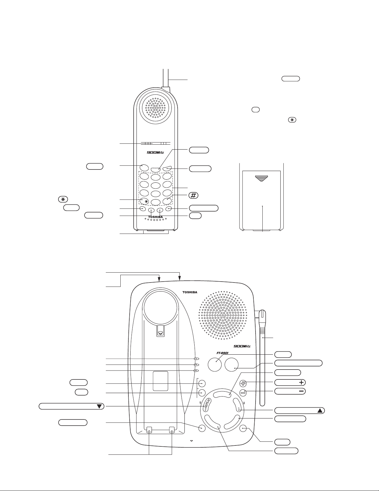
OPERATING CONTROLS
HANDSET CONTROLS AND FUNCTIONS
Antenna
TALK
TALK/BATT LOW LED
TALK Button
(TONE MODE) Button
MEM (Memory) Button
MUTE Button
/ BATT LOW
COMPANDOR NOISE REDUCTION
RLD/P
TAL K
1
ABC
2
GHI
4
JKL
5
PQ
RS
TUV
7
8
TONE
OPER
0
MEM
MUTE
RDL/P (Redial/Pause)Button
FLASH
DEF
3
MNO
6
WX
9
YZ
#
VOL/RING
CH
FLASH Button
Dialpad
VOL/RING Button
CH (channel)Button
SETTING THE DIAL MODE
1 Press and hold
2 To set the dial mode for pulse dialing,
(PULSE MODE)
Button
FLASH
until you hear
a confirmation tone.
press
tone dialing press
#
. Or to set the dial mode for
. A confirmation
tone sounds to indicate the setting is
complete.
Charging contact
BASE UNIT CONTROLS AND FUNCTIONS
DC IN 9V Jack
TEL LINE Jack
COMPANDOR NOISE REDUCTION
POWER LED
IN USE LED
CHARGE LED
MENU Button
SET Button
REW REPEAT/SELECT
Button
GREETING Button
POWER
IN USE
CHARGE
MENU
SET
SELECT SELECT
GREETING
ALL DIGITAL ANSWERING SYSTEM
CORDLESS TELEPHONE
PAG E
MEMO/2WAY
W
S
E
R
N
A
D
E
L
E
T
E
P
Rechargeable
Battery Pack(back)
REC
VOLUME
S
K
I
P
P
O
T
S
TIME
/
Y
A
L
Antenna
PAGE Button
REC MEMO/2WAY Button
ANSWER Button
VOLUME Button
VOLUME Button
SKIP FF/SELECT Button
PLAY/STOP Button
Charging Contact
MIC
— 2 —
TIME Button
DELETE Button
Page 4
SETTING THE CLOCK
1. Press
MENU
twice, then press
ANSWERING MACHINE
SET
.
2. Select the day of the week by pressing
SET
press
3. Select the hour by pressing
SET
4. Select the minute by pressing
press
5. Select AM/PM by pressing
.
SELECT
.
SELECT
SET
.
SELECT
SELECT
or
or
SELECT
or
SELECT
SELECT
or
. When the correct day is announced,
. When the correct hour is announced, press
SELECT
. When the correct minute is announced,
. When AM or PM is announced, press
RECORDING AND SETTING THE GREETING MESSAGE
To record the greeting message:
1. Press
MENU
once, then press
2. Start to record your message after the guidance.
3. Press
REC MEMO/2WAY
or
To change the greeting message:
1. Press
2. Press
GREETING
SELECT
.
or
SELECT
REC MEMO/2WAY
PLAY/STOP
to finish recording.
to change to other.
.
SET
.
3. Press
PLAY/STOP
to exit the system.
SETTING THE SECURITY CODE (PIN):
1. Press
2. Press
3. Press
4. Press
MENU
three times.
SET
to change the security code (PIN).
SELECT
SET
to set the security code (PIN).
or
SELECT
until the desired number appears.
— 3 —
Page 5
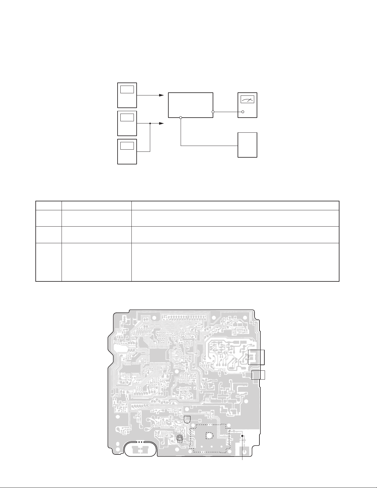
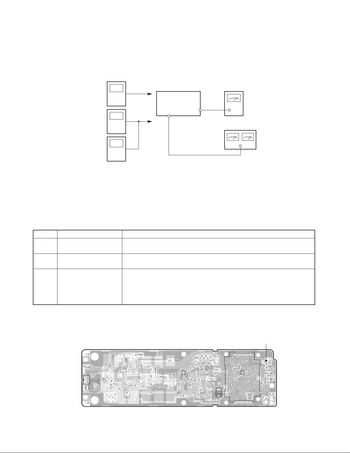
ALIGNMENT PROCEDURE
Base Unit
Transmitter Section
Connections
RF
Power
Meter
Frequency
Counter
Deviation
Meter
Test Point
RF
Test Point
Preset
Press and hold the “ANSWER” key about 5.0 seconds while turning the 7. SEG LED shows “8” .
Alignment Procedure
BASE Unit
J2
DC IN
9V Jack
TEL Line
Jack
J1
1kHz -15dBm
AF GEN.
AC
Adapter
AC 120V
60Hz
step
1
2
Adjustment
RT301
(TX Power)
CT1
(TX Frequency)
Remarks
Connect the Power Meter to the RF test point on the Base MAIN PCB.
Adjust RT301 for a -6.0dBm reading on the Power Meter.
Connect the Frequency Counter to the RF test point on the Base MAIN
PCB. Adjust CT1 to make sure that the frequency is 926.897468 MHz.
Press the “SKIP / FF” key to enter the TEST MODE “9”. Connect the AF
3
RT3
(TX Modulation)
Generator to the TEL Line Jack on the Base Main PCB. Make sure that
the output is 1 kHz -15dBm from the AF Generator.
Connect the Deviation Meter to the RF test point on the Base MAIN PCB.
Adjust RT3 to indicate ±8 kHz Dev.
Alignment Point Location on Base Main PCB and Base RF PCB
Base Main PCB
J1
J2
TEL LINE Jack
DC IN 9V Jack
CT1
— 4 —
RT3
Base RF PCB
RT301
RF Test Point
Page 6
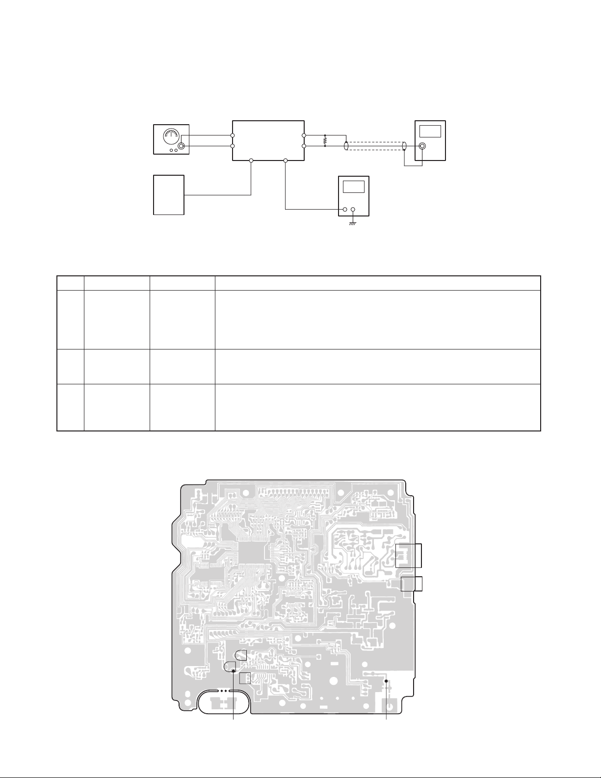
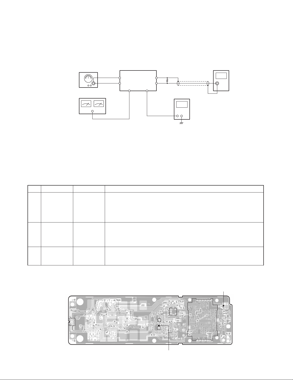
Receiver Section
Connections
RF SG
-
+
RF
Test Point
TEL Line
Jack
J1
Dummy Load
(600-ohm)
-
+
AC VoltmeterBASE Unit
AC 120V
60Hz
AC
Adapter
DC IN 9V Jack
J2
AF
Test Point
DC Voltmeter
Preset
Place the Base Unit in RX SENS mode (step 11) in accordance with the precedure on page 4.
Alignment Procedure
step
Preset to
1
SG: 1mV
No modulation
SG: 1mV
2
1 kHz ±8kHz
deviation
SG: -113dB
3
No modulation
Adjustment
(Discriminator
Voltage)
(RX AF
Voltage)
µµ
µV
µµ
(SQ Point)
L4
RT2
RT1
Remarks
Connect the RF Signal Generator to the RF test point on the Base MAIN
PCB. Make sure that the frequency is 902.952467 MHz.
Connect the DC Voltmeter to the AF test point. Adjust L4 to indicate DC
1.00 V.
Connect the AC Voltmeter across a 600-ohm dummy to the Telephone Line
Jack. Adjust RT2 for a -12dBm reading on the AC voltmeter.
Press thePress the “SKIP / FF” key to enter the TEST Mode 12.
Make sure that thefrequency of RF SG output is 902.952467 MHz.
Adjust RT1 to turn to thepoint where the LED indication is just vibrated.
Alignment Point Location on Base Main PCB and Base RF PCB
Base Main PCB
RT1
RT2
L4
RF Test PointAF Test Point
J1
J2
TEL LINE Jack
DC IN 9V Jack
— 5 —
Page 7
Handset Unit
Transmitter Section
Connections
Power
Meter
Frequency
Counter
Deviation
Meter
RF
Test Point
RF
Test Point
HANDSET Unit
J601
Battery
Connector
MIC+Pin
DC 3.8V
AF GEN.
1kHz 9mV
DC Power Supply
Preset
a) Connect the handset RF unit to the handset main unit.
b) Connect DC power supply to battery connector on the handset unit.
c) Turn the DC power supply ON while pressing “ ∗ ” and “ # ” keys, and keep pressing the keys continuously for
approximate 2 seconds.
d) Release keys when entering TEST mode 1 with TALK LED lightning and beep.
Alignment Procedure
step
1
2
3
Adjustment
RT501
(TX Power)
CT601
(TX Frequency)
RT603
(TX Modulation)
Remarks
Connect the RF power Meter to the RF test point on the handset MAIN PCB.
Adjust RT501 for a -6.0dBm reading on the Power Meter.
Connect the Frequency Counter to the RF test point on the handset MAIN
PCB. Adjust CT601 to make sure that the frequency is 903.052467 MHz.
Press the “2” key to enter the TEST Mode 2. Connect the AF Generator to
the MIC Connector. Make sure that the output is 1kHz 9mV from the AF
Generator.
Connect the Deviation Meter to the RF test point on the handset MAIN PCB.
Adjust RT603 to indicate ±8 kHz Dev.
Alignment Point Location on Handset Main PCB and Handset RF PCB
Handset PCB
RF PCB
RT501
J601
RT603
MC601
CT601
— 6 —
RF Test Point
Page 8
Receiver Section
Connections
RF SG
DC Power Supply
RF
Test PointSPTerminal
+
J601
Battery
Connector
DC 3.8V
Dummy Load
WHT
BLK
AF
Test Point
(150-ohm)
DC Voltmeter
AC VoltmeterHANDSET Unit
Preset
a) Connect the handset RF unit to the handset main unit.
b) Connect DC power supply to battery connector on the handset unit.
c) Turn the DC power supply ON while pressing “ ∗ ” and “ # ” keys, and keep pressing the keys continuously for
approximate 2 seconds.
d) Release keys when entering TEST mode 1 with TALK LED lightning and beep.
Alignment Procedure
step
Preset to
1
SG: 1mV
No modulation
SG: 1mV
1 kHz ±8kHz
2
deviation
SG: -6.0 dBµV
1kHz ±8kHz
3
Deviation
Adjustment
L602
(Discriminator
Voltage)
RT602
(RX AF
Voltage)
RT601
(SQ Point)
Remarks
Press the “4” key to enter the TEST Mode 4. Connect the RF Singal
Generator to the RF test point on the handset MAIN PCB. Make sure that
the frequency is 926.997467 MHz.
Connect the DC Voltmeter to the AF test point. Adjust L602 to indicate
DC 0.85 V.
Connect the RF Signal Generator to the RF test point on the handset MAIN
PCB. Make sure that the frequency is 926.997467 MHz.
Connect the AC Voltmeter across a 150-ohm dummy to the SP Terminal.
Adjust RT602 for a 90 mV reading on the AC Voltmeter.
Press the “5” key to enter the TEST Mode 5. Make sure that the frequency
of RF SG output is 926.997467 MHz. Adjust RT601 to turn to the point
where the indication is just vibrated.
Alignment Point Location on Handset Main PCB and Handset RF PCB
Handset PCB
L602
RF PCB
RT602
J601
RT601
AF Terminal
— 7 —
RF Test Point
Page 9
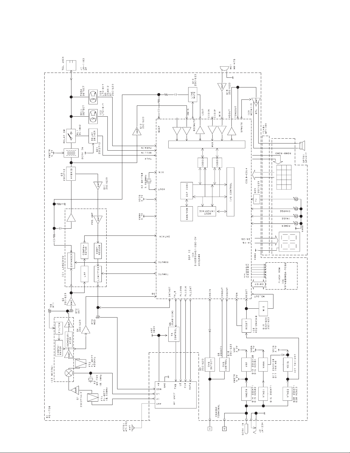
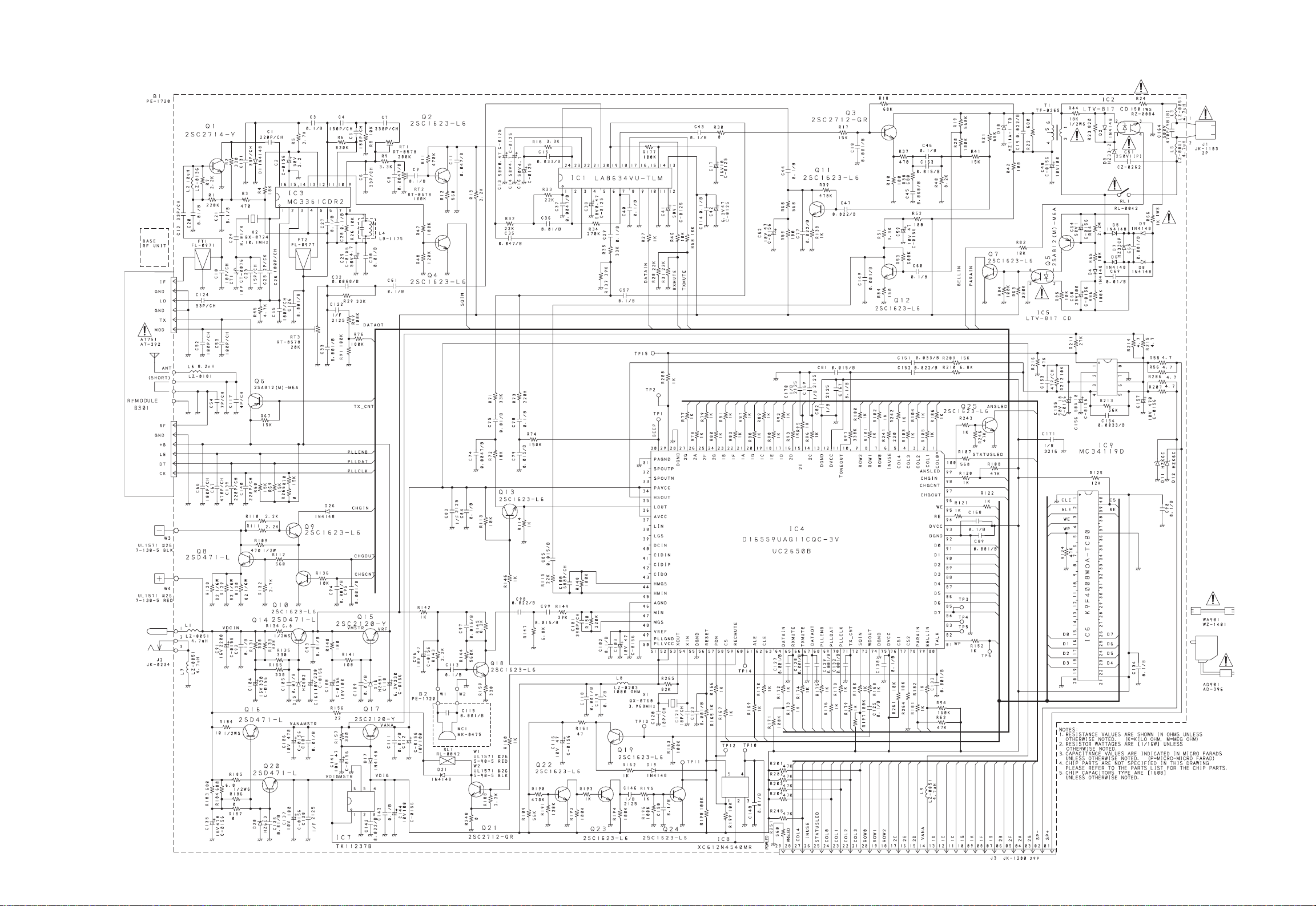
Base Unit
BLOCK DIAGRAMS
— 8 —
Page 10
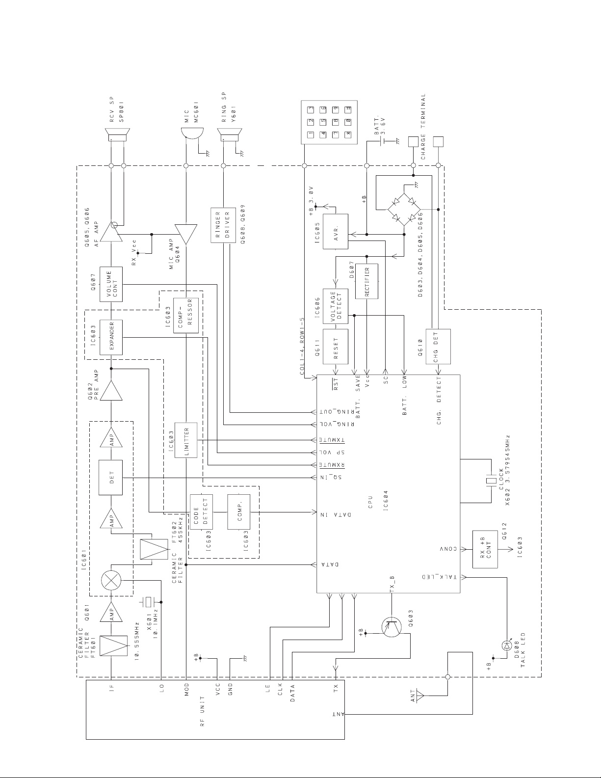
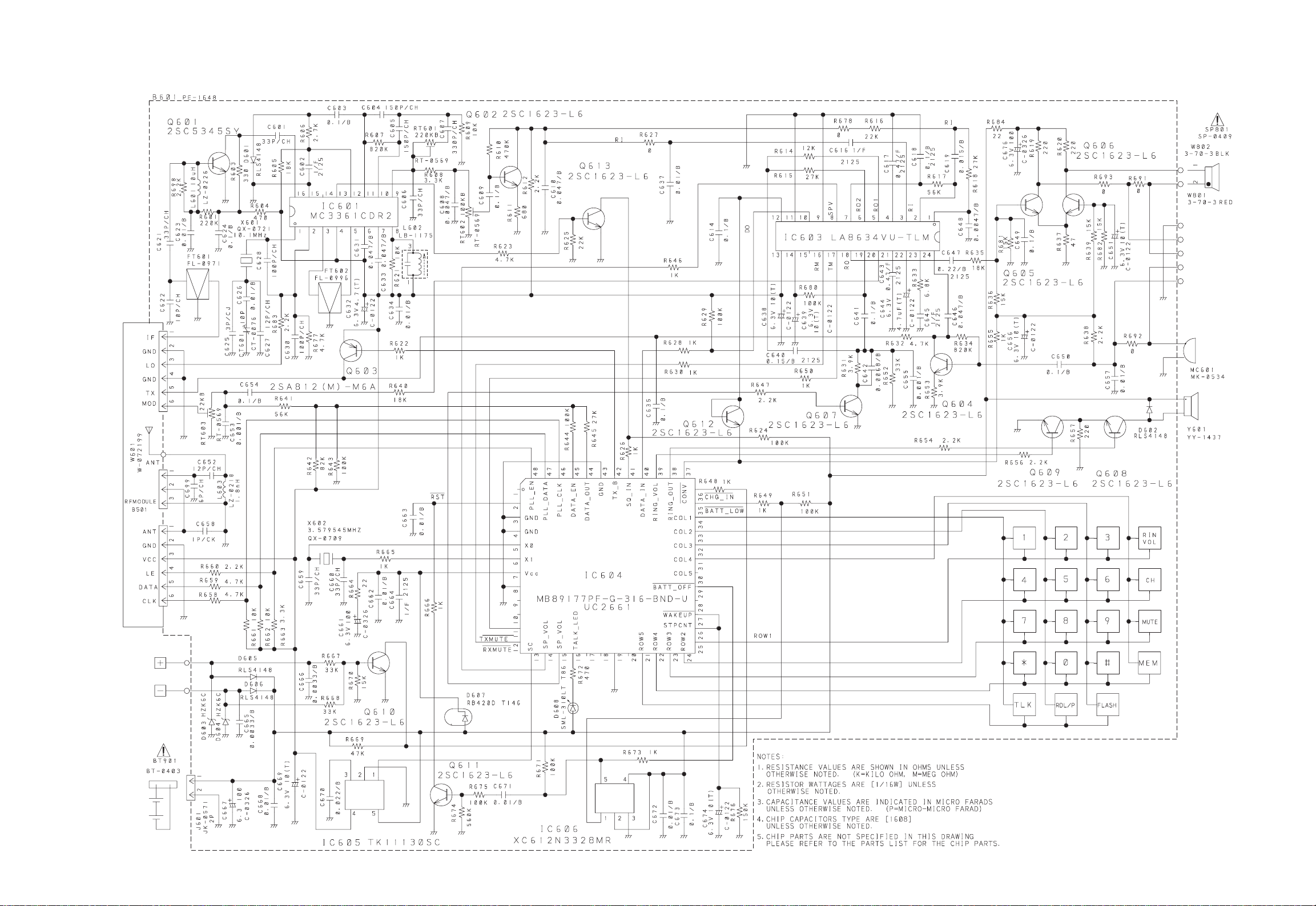
Handset
— 9 —
Page 11
Base Unit
SCHEMATIC DIAGRAMS
— 10 — — 11 —
Page 12
Handset
— 12 — — 13 —
Page 13
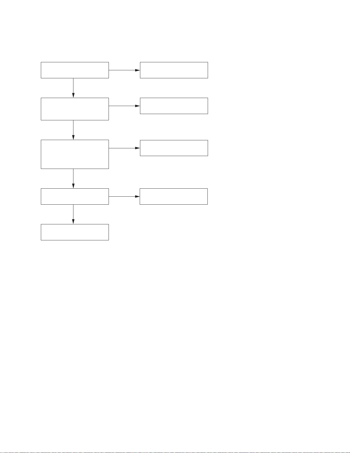
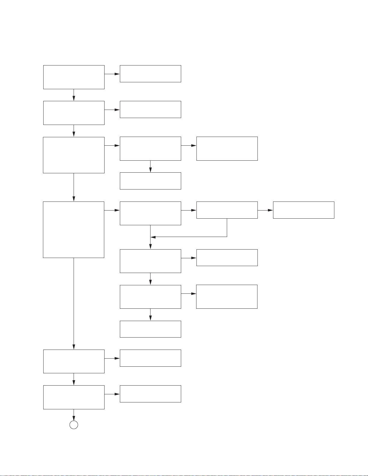
TROUBLESHOOTING HINTS
1. The bell does not ring.
Check RINGER mode setting
is Hi or Low.
OK
When the PAGE SW of the
base is pressed, does the
ringer on the handset ring?
OK
When the TEL SG is joined
with the base to make bell
signal, is there pulse wave at
pin 4 of IC2?
OK
Is there pulse wave at
pin 79 of IC4?
OK
Check IC4 and its
peripheral circuit.
NG
NG
NG
NG
Set RINGER volume setting
to Hi or Low.
See 2. The bell does not ring
& page does not ring.
Check IC2 and TEL network
circuit.
Check R82, R182 and R94.
If you want to reset the unit to the factroy settings
You can cancel the OGM, PIN, and the clock settings by the following process.
1 Disconnect the AC adaptor and telephone line cord from the base. Keep the AC adaptor connected to the wall
outlet. Make sure that the telephone line cord remains disconnected during this procedure.
2
While pressing the DELETE button, plug the AC power adaptor into the base. Keep pressing the DELETE
button for more than 5 seconds.
A beep sounds and “ P” blinks in the LED display.
To resume using the unit, connect the telephone line cord and place the handset on the base.
Note:
If you turn on the unit again, “ P” may flash.
— 14 —
Page 14
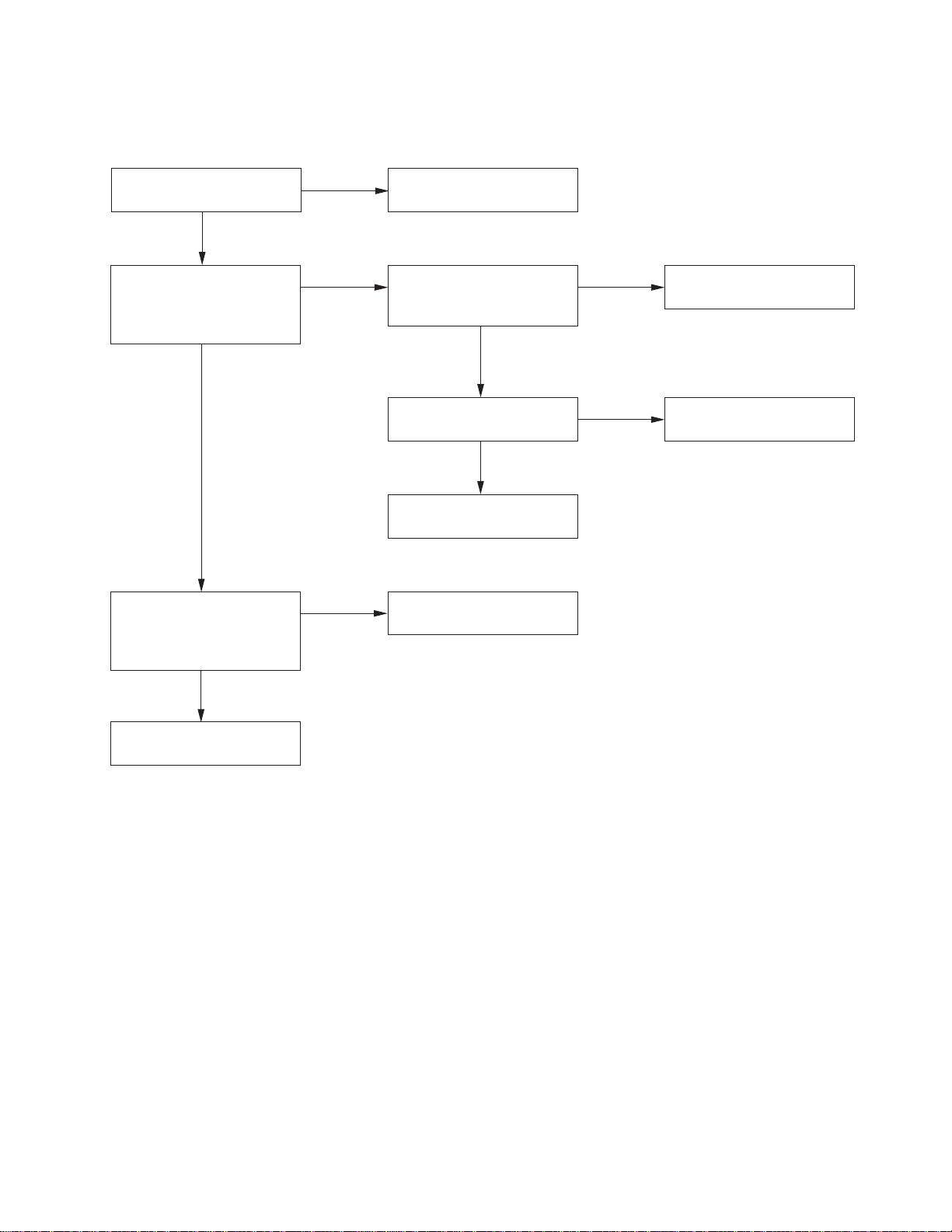
2. The bell does not ring & page does not ring.
Can the base and handset be
connected?
OK
Press handset DIAL key
while in TALK MODE.
Can key touch sound be
heard from the ringer?
OK
When the PAGE SW of the
base is pressed, does pin67
of IC4 change from high to
low?
NG
NG
NG
See 3. The base and handset
cannot be connected.
When the key of the handset is
pressed, can the pulse output
at pin 38 of IC604 be seen?
OK
At the Q608 collector, can the
pulse wave be seen?
OK
Check RINGER Y601.
Check DSP unit.
NG
NG
Check IC604.
Check R654, R656, R657,
Q609, Q608 and D602.
Check IC4 and its peripheral
circuit.
OK
— 15 —
Page 15
3. The base and handset cannot be connected.
Check whether the base
is able to set in the test
mode 8.
OK
NGACheck IC4 and its
peripheral circuit.
Check base RF unit.
NG
Check the TX POWER
and the TX FREQUENCY
on the base unit.
OK
OK
NG
Check base RF unit.
NG Check whether there is a
250 Hz data waveform at
“MOD” of RF unit.
Check RT3, R76, R91,
R49, C129, C122,
C33 and C52.
NG
OK
Check base RF unit.
OK
NG Check whether there is a
250 Hz data waveform at
RT2 AF test point.
Check IC3, Q1 and their
peripheral circuit.
NG
OK
Check whether there is a
250 Hz data waveform at
the Q2 collector.
Check RT2, Q2 and their
peripheral circuit.
NG
OK
Check whether there is a
250 Hz data waveform at
pin 64 of IC4.
NG
OK
Check IC4 and its
peripheral circuit.
Check whether the
handset is able to set in
the test mode 1.
OK
NG
Check IC604 and its
peripheral circuit.
Check the TX POWER
and the TX FREQUENCY
on the handset unit.
OK
NG
Check handset RF unit.
OK
Check R27, R171, R172,
IC1 and their peripheral
circuit.
Set the base in the test
mode 10, check
whether deviation of the
TX data is app. 9.0 kHz
Dev.
Set the base in the test
mode 13,
902.952467MHz
(250 Hz ±8 kHz Dev.)
1mV output signal from
RF test point is
applied. Does the
CHARGE LED light?
— 16 —
Page 16

A
Check handset RF unit.
Set the handset in the
test mode 3, check
whether deviation of the
TX data is app. 9.0 kHz
Dev.
NG Check whether there is a
250 Hz data waveform at
“MOD” of RF unit.
Check RT603, R641,
R642, R643, R644,
R645 and C653.
NG
OK
Check handset RF unit.
NG
Set the handset in the
test mode 6, 926.997467
MHz (250 Hz ±8 kHz
Dev.) 1mV output signal
from RF test point is
applied. Check whether
the bell ring.
NG
Check whether the 250
Hz data waveform from
pin 9 of IC601 is fed.
Check IC601, Q601 and
their peripheral circuit.
NG
OK
OK
Check whether there is a
250 Hz data waveform at
the Q602 collector.
Check RT602, Q602 and
their peripheral circuit.
NG
OK
Check whether there is a
250 Hz data waveform at
pin 40 of IC604.
Check R628, R629,
IC603 and their
peripheral circuit.
NG
OK
Check IC604 and its
peripheral circuit.
OK
Place the handset on the
base to charge about 5
seconds, then connect
again.
OK
— 17 —
Page 17

4. Cannot make a phone call (pulse).
Can the base and handset
be connected?
OK
While in TALK MODE, press
dial key of the handset.
Check whether square
waveform from pin 80 of
IC4 is fed.
OK
Check Q21, RL1 and their
peripheral circuits.
NG
NG
5. Cannot make a phone call (tone).
See 3. The base and handset
cannot be connected.
Check IC4.
Can the base and handset be
connected?
OK
While in TALK MODE, press
dial key of the handset.
Can tone waveform from Pin
36 of IC4 is fed?
OK
Can tone signal be heard
from the handset speaker?
OK
Check the base TEL-line
circuit and RELAY control
circuit.
NG
NG
NG
See 3. The base and handset
be cannot be connected.
Check IC4.
Check Q13, IC1, Q3 and
their peripheral circuits.
— 18 —
Page 18

6. Voice cannot be transmitted to other party (outgoing call).
Can the base and handset be
connected?
OK
The 1 kHz, 9.0mV sine
waveform is applied to
+
MC601
sine waveform from pin 24 of
IC603 be fed?
Check whether there is the
1 kHz sine waveform at
pin 20 of IC603.
Check whether there is the
1 kHz sine waveform at
“MOD” RF unit.
TX output signal from the
handset is detected by the
liner detector, can the 1 kHz
sine waveform be fed?
side, can the 1 kHz
OK
OK
OK
OK
NG
NG
NG
NG
NG
See 3. The base and handset
cannot be connected.
Check Q604 and its
peripheral circuit.
Check IC603 and its
peripheral circuit.
Check RT603 and its
peripheral circuit.
Check handset RF unit.
Check whether there is the
1 kHz sine waveform at pin 9
of IC3 on the base unit.
OK
Check whether there is the
1 kHz sine waveform at pin 3
of IC1.
OK
Check whether there is the
1 kHz sine waveform at
pin 6 of IC1.
OK
Check whether there is the
1 kHz sine waveform at the
Q3 collector.
OK
Check whether the 1 kHz sine
waveform from TEL-line
output is fed.
OK
Check MC601 of handset.
NG
NG
NG
NG
NG
Check IC3, Q1 and their
peripheral circuit.
OK
Check RT2, Q2 and their
peripheral circuits.
Check IC1 and its
peripheral circuit.
Check IC1, Q3 and its
peripheral circuit.
Check T1, RL1 and their
peripheral circuits.
NG
Check base RF unit.
— 19 —
Page 19

7. The voice of the caller cannot be heard (incoming call).
Can the base and handset be
connected?
OK
The 1 kHz, -15dBm sine
waveform is applied to TELline of the base, can the 1 kHz
sine waveform from the Q3
collector be fed?
OK
Check whether there is the
1 kHz sine waveform at
pin 24 of IC1.
OK
Check whether there is the
1 kHz sine waveform at
pin 20 of IC1.
OK
Check whether there is the
1 kHz sine waveform at
“MOD” RF unit.
OK
NG
NG
NG
NG
NG
See 3. The base and handset
cannot be connected.
Check the base TEL-line
circuit and REPLAY control
circuit.
Check Q11 and its peripheral
circuit.
Check IC1 and its peripheral
circuit.
Check RT3 and its
peripheral circuit.
TX output signal from the
base is detected by the liner
detector, can the 1 kHz sine
waveform be fed?
OK
Check whether there is the
1 kHz sine waveform at pin 9
of IC601 on the handset unit.
OK
Check whether there is the
1 kHz sine waveform at pin 3
of IC603.
OK
Check whether there is the
1 kHz sine waveform at the
pin 18 of IC603.
OK
Check whether there is the
1 kHz sine waveform at pin
1, 2 of SP801.
OK
NG
NG
NG
NG
NG
Check base RF unit.
Check IC601, Q601 and
their peripheral circuit.
OK
Check RT602, Q602 and
their peripheral circuits.
Check IC603 and its
peripheral circuit.
Check Q605, Q606 and its
peripheral circuit.
NG
Check handset RF unit.
Check SP801 and W801,
W802.
— 20 —
Page 20

IC AND TRANSISTOR VOLTAGE CHART
TRANSISTORS Unit [V] Unit [V]
Ref.
Pin STBY TALKNote
No.
E 0.0 0.0
Q1 C 2.4 2.1-2.5
B 0.7 0.7
E 0.4-0.6 0.5
Q2 C 3.1-3.5 3.2
B 1.0-1.3 1.1
E 1.0 1.0
Q3 C 3.9 3.9
B 1.7 1.7
E 0.0 0.1
Q4 C 0-3.6 3.6
B 0.5 0.0
E 0.0 0.0
Q5 C 0.0 0.0
B 0.0 0.0
E 3.3 3.3
Q6 C 0.0 3.2
B 3.3 2.5
E 0.0 0.0
Q7 C 0.0 0.0
B 0.6 0.6
E 0.1 0.0
Q8 C 0.1 0.0
B 0.8 0.0
E 0.0 0.0
Q9 C 3.5 3.5
B 0.1 0.0
E 0.0 0.0
Q10 C 0.0 0.0
B 0.7 0.7
E 1.2 1.2
Q11 C 4.4 4.4
B 1.9 1.9
E 0.1 0.1
Q12 C 2.5 2.5
B 0.7 0.7
E 1.5 1.5
Q13 C 0.1 0.1
B 0.3 0.3
E 5.2 5.2
Q14 C 8.7 8.5
B 5.9 5.9
E 3.3 3.2
Q15 C 5.2 5.2
B 3.9 3.9
E 5.6 5.6
Q16 C 8.8 8.7
B 6.2 6.2
E 3.6 3.6
Q17 C 5.6 5.6
B 4.3 4.3
Note
Ref.
Pin STBY TALKNote
No.
E 0.1 0.1
Q18 C 1.5 1.5
B 0.7 0.7
E0 0
Q19 C 2.32 2.6/3.3
B -3.1/0.6 -3.6/0.8
E 5.6 5.6
Q20 C 8.9 8.6
B 6.2 6.2
E0 0
Q21 C 9.1 0
B0 0.7
E0 0
Q22 C 0.6 0.6
B0 0
E0 0
Q23 C0 0
B 0.6 0.6
E0 0
Q24 C 3.7 3.7
B0 0
E0 0
Q25 C 2.5 2.5
B 0.8 0.8
E 0 GND 0 GND
Q601 C 0-2.2 PULSE 2.2
B 0-0.7 PULSE 0.7
E 0-0.6 PULSE 0.4
Q602 C 0-2.0 PULSE 1.8
B 0-1.0 PULSE 1
E 0-3.0 PULSE 3
Q603 C 0.2 3
B 0-2.5 PULSE 2.2
E0 0.9
Q604 C 0.2 2
B 0.2 1.4
E0 0.7
Q605 C 3.8 2
B0 1.4
E0 0.7
Q606 C 3.8 1.8
B0 1.4
E 0 GND 0
Q607 C0 0
B0 0
E0 0
Q608 C 3.8 3.8
B0 0
E0 0
Q609 C0 0
B0 0
Note
Vol:MEDIUM
Vol:MEDIUM
Vol:MEDIUM
— 21 —
Page 21

Ref.
Pin STBY TALKNote
No.
E0 0
Q610 C 3.8 3.8
B 0 w/o CHG 0
E 0 GND 0 GND
Q611 C 3.6 3.5
B0 0
E 0 3.5
Q612 C 0-0.6 PULSE 1.6
B 0-0.6 PULSE 1.6
E 0 GND 0 GND
Q613 C 0-3.8 PULSE 3.8
B 0-0.7 PULSE 0
Unit [V] IC's Unit [V]
Ref.
Note
Pin STBY TALKNote
No.
1 3.2 3.2
2 3.2 3.2
3 2.7 2.7
4 0.7 0.6
5 2.7 2.7
6 2.7 2.7
7 3.1 3.1
8 5.1 5.1
9 0.0 GND 0.0 GND
10 3.5-0.0
11 0.0 GND 0.0 GND
12 2.7 2.7
IC1 13 5.2 Vcc 5.2 Vcc
14 2.7 2.7
15 2.7 2.7
16 0.5 3.7
17 0.5 3.7
18 2.7 2.7
19 2.7 2.7
20 2.7 2.7
21 0.5 0.6
22 2.7 2.7
23 2.7 2.7
24 2.7 2.7
1 0.0 0.0
2 0.0 0.0
IC2
3 0.0 GND 0.0 GND
4 3.6 3.6
1 3.9-2.5 X'TAL 3.9-2.5 X'TAL
2 3.1-2.3 X'TAL 3.1-2.3 X'TAL
3 2.6 2.9
4 3.3 Vcc 3.3 Vcc
5 2.2 2.4-2.0
6 2.2 2.2
7 2.2 2.2
IC3 8 3.4-3.2 3.4-3.2
9 0.9 0.9
10 0.9 0.9
11 2.1-0.8 1.5
12 0.5 0.8
13 3.2 0.0
14 0.0 0.0
15 0.0 GND 0.0 GND
16 1.9 2.1-1.7
1 3.7 COL00 3.7 COL00
2 3.7 COL01 3.7 COL01
3 3.7 COL02 3.7 COL02
IC4 4 3.7 COL03 3.7 COL03
5 3.7 COL04 3.7 COL04
6 2.7 INUSE_LED 0.2 INUSE_LED
7 0.0 ROW00 0.0 ROW00
DATA(PULSE)
3.5-0.0
Note
DATA(PULSE)
— 22 —
Page 22

IC's Unit [V] Unit [V]
Ref.
Pin STBY TALKNote
No.
8 0.0 ROW01 0.0 ROW01
9 0.0 ROW02 0.0 ROW02
10 0.0 0.0
11 0.0 TONE_OUT 0.0 TONE_OUT
12 3.7 Dvcc 3.7 Dvcc
13 0.0 DGND 0.0 DGND
14 2.3 2.3
15 2.3 2.3
16 2.3 2.3
17 2.3 2.3
18 2.3 2.3
19 2.3 2.3
20 2.3 2.3
21 2.3 2.3
22 2.3 2.3
23 2.3 2.3
24 2.3 2.3
25 2.3 2.3
26 2.3 2.3
27 2.3 2.3
28 0.0 DGND 0.0 DGND
29 3.0 3.0
30 0.0 0.0
31 0.0 GND 0.0 GND
32 1.5 1.5
IC4 33 1.5 1.5
34 3.7 Vcc 3.7 Vcc
35 1.5 1.5
36 0.3 0.3
37 3.7 AVcc 3.7 AVcc
38 0.0 0.0
39 3.7 3.7
40 0.0 0.0
41 0.0 0.0
42 0.0 0.0
43 3.7 3.7
44 1.5 1.5
45 1.5 1.5
46 0.0 0.0
47 1.5 1.5
48 1.5 1.5
49 1.5 Vref 1.5 Vref
50 0.0 PLLGND 0.0 PLLGND
51 3.7 PLLVcc 3.7 PLLVcc
52 3.7 PLLVcc 3.7 PLLVcc
53 1.1-0.0 X'TAL 1.1-0.0 X'TAL
54 1.4-0.0 X'TAL 1.4-0.0 X'TAL
55 0.0 DGND 0.0 DGND
56 3.7 RESET 3.7 RESET
57 3.7 PDN 3.7 PDN
58 3.7 3.7
Note
Ref.
Pin STBY TALKNote
No.
59 0.0 0.0
60 0.0 0.0
61 0.0 0.0
62 0.0 0.0
63 3.7 3.7
64 3.5-0.0 DATA_IN 3.5-0.0 DATA_IN
65 0.0 RX_MUTE 3.7 RX_MUTE
66 0.0 TX_MUTE 3.7 TX_MUTE
67 0.0 0.0
68 3.2-0.0 PLLENB 3.2 PLLENB
69 3.2-0.0 PLLDAT 0.0 PLLDAT
70 3.2-0.0 PLLCLK 0.0 PLLCLK
71 3.3 TX_CONT 0.1 TX_CONT
72 0.0 3.6
73 3.5-0.0 WD_OUT 3.5-0.0 WD_OUT
74 0.0 DGND 0.0 DGND
75 3.7 DVcc 3.7 DVcc
76 3.7 3.7
77 0.0 0.0
78 0.0 0.0
79 3.7 BELL_IN 3.7 BELL_IN
80 0.0 TALK 3.5 TALK
IC4 81 3.7 3.7
82 0.0 0.0
83 0.0 0.0
84 0.0 0.0
85 0.0 0.0
86 0.0 0.0
87 0.0 0.0
88 0.0 0.0
89 0.0 0.0
90 0.0 0.0
91 0.0 0.0
92 0.0 DGND 0.0 DGND
93 3.7 DVcc 3.7 DVcc
94 3.7 3.7
95 3.7 3.7
96 3.5 CHG_OUT 0.0 CHG_OUT
97 3.7 3.7
98 3.7 3.7
99 3.5 3.5
100 2.4 2.4
1 0.0 0.0
2 0.0 0.0
IC5
3 0.0 GND 0.0 GND
4 0.6 0.6
1 0.0 CLE(GND) 0.0 CLE(GND)
2 0.0 0.0
IC6 3 0.0 0.0
4 3.9 3.9
5 3.8 3.8
Note
— 23 —
Page 23

Unit [V] Unit [V]
Ref.
Pin STBY TALKNote
No.
6 0.0 0.0
7 0.0 0.0
8 0.0 0.0
9 0.0 0.0
10 0.0 0.0
11 0.0 0.0
12 0.0 0.0
13 0.0 0.0
14 0.0 0.0
15 0.0 0.0
16 0.0 0.0
17 0.0 0.0
18 0.0 0.0
19 0.0 0.0
IC6 20 0.0 GND 0.0 GND
21 3.9 Vcc 3.9 Vcc
22 0.0 0.0
23 0.0 0.0
24 0.0 0.0
25 0.0 0.0
26 0.0 0.0
27 0.0 0.0
28 0.0 0.0
29 0.0 0.0
30 0.0 0.0
31 0.0 0.0
32 0.0 0.0
33 0.0 0.0
34 0.0 0.0
35 0.0 0.0
36 0.0 0.0
37 0.0 0.0
38 3.9 3.9
39 3.9 3.9
40 3.9 Vcc 3.9 Vcc
1 5.6 5.6
2 0.0 GND 0.0 GND
3 1.2 1.2
IC7
4 3.7 3.7
5 0.0 GND 0.0 GND
6 5.6 5.6
1 3.7 3.7
2 5.6 5.6
IC8 3 0.0 GND 0.0 GND
4 5.6 5.6
5 3.7 3.7
1 2.9 2.9
2 2.4 2.4
IC9 3 2.4 2.4
4 2.4 2.4
5 2.4 2.4
Note
Ref.
Pin STBY TALKNote
No.
6 5.5 5.5
IC9 70 0
8 2.4 2.4
1 0/SineWave 10.1MHz SineWave 10.1MHz
2 0/SineWave 10.1MHz SineWave 10.1MHz
3 0-2.4 PULSE
4 0-3.0 PULSE 3.0 Vcc
5 0-2.6 PULSE SineWave 455kHz
6 0-2.6 PULSE 2.6
7 0-2.6 PULSE 2.6
IC601
IC603 11 0 GND 0 GND
IC604
8 0-3.0 PULSE 3.0
9 0 0.85 NOISE
10 0-0.7 PULSE 0.6
11 0-0.7 NOISE 0.7
12 0-0.5 PULSE 0.8
13 0-2.9 PULSE 0
14 0 0
15 0 GND 0 GND
16 0-3.0 PULSE 3.0
1 0-1.8 NOISE 1.8
2 0-1.8 NOISE 1.8
3 0-1.3 NOISE 0.6
4 0 0.6
5 0 1.6
6 0 1.6
7 0-1.8 PULSE 1.8
8 0 3.5
9 0 GND 0 GND
10 0-3.0 PULSE 0.1-3.0 PULSE
12 0-0.6 PULSE 1.6
13 0-3.0 PULSE 3.0 Vcc
14 0 1.6
15 0 1.6
16 0 3.5
17 0 3.5
18 0 1.6
19 0 1.6
20 0 1.6
21 0 0.6
22 0.3 1.6
23 0.3 1.6
24 0 1.6
10 0
2 3.6 0
3 0 GND 3 GND
4 0 GND 3 GND
5 0/SineWave 3.58MHz SineWave
6
3.6 sineWave
7 3.6 Vcc 3.5 3.58MHz
8 0 GND 0
3.58MHz SineWave 3.58MHz
ClippedWave
Note
455kHz
Vol:MEDIUM
— 24 —
Page 24

Unit [V]
Ref.
Pin STBY TALKNote
No.
90 0
10 0 0
11 0 3.5
12 0 3.5
13 0-3.6 PULSE 3.5
14 0 3.5
15 0 0
16 3.6 0.3
17 0 0
18 0 0
19 0 GND 0 GND
20 0 0
21 0 0
22 0 0
23 0 0
24 0 0
25 0 0
26 1.0-3.0 3.5
27 1.0-3.0 3.5
IC604 28 0 0
29 3.8 3.8
30 3.6 3.5
31 3.6 3.5
32 3.6 3.5
33 3.6 3.5
34 3.6 3.5
35 3.8 3.8
36 3.8 3.8
37 0 3.5
38 0 0
39 0 0
40 0-3.0 PULSE 0-3.0 NOISE
41 0-3.8 PULSE 3.8
42 0-2.5 PULSE 0.2
43 0 GND 0 GND
44 0-0.8 PULSE 0.8
45 0 0
46 0-3.0 PULSE 3.0
47 0-3.0 PULSE 3.0
48 0-3.0 PULSE 3.0
1 0-3.5 PULSE 3.5
2 0 GND 0 GND
IC605 3 0-1.3 PULSE 1.3
4 0-3 PULSE 3
5 3.8 BATT:3.8V 3.8 BATT:3.8V
1 3.8 BATT:3.8V 3.8 BATT:3.8V
2 3.8 BATT:3.8V 3.8 BATT:3.8V
IC606 3 0 GND 0 GND
4 3.8 BATT:3.8V 3.8 BATT:3.8V
5 3.8 BATT:3.8V 3.8 BATT:3.8V
Note
Vol:MEDIUM
Vol:MEDIUM
— 25 —
Page 25

DIODES
SEMICONDUCTOR LEAD IDENTIFICATION
1N4148
HZ33-2
HZ33CP
HZ4B1
Anode
HZ6B2
HZ6C3
HZ11A
SML-310LT
SML-310MT
Cathode
TRANSISTOR
2SD471
Cathode
Anode
RLS4148
HZK6C
Cathode
RB420D
2SC2120
Cathode
ELD406
Anode
Cathode G1
Cathode A1
Cathode F1
Cathode B1
Cathode B2
Cathode F2
Cathode A2
A2
G2
C2
D2
Cathode E2
Cathode D2
Cathode G2
B2
Cathode C2
16 15 14 13 12 11 10 9
DIGIT 1 DIGIT 2
F1
E1
12345678
(Open)Anode
Cathode C1
A1
C1
G1
E2
D1
Cathode E1
Cathode D1
B1
F2
Anode 1
Anode 2
2SC2714
2SC1623
2SC2712
2SC5345
2SA812(M)
B
E
IC's
IC1
IC603
LA8634VU
PRE. IN24
1LPF1 IN
E
E
C
B
IC3
IC601
MC3361CDR2
PRE. NF23
CMP. NF22
CMP. VREC21
CMP. OUT20
LPF2 IN19
LPF2 OUT18
CMP. MUTE CONT17
EXP. MUTE CONT16
TX. DATA IN15
VREF14
VCC13
2LPF1 OUT
3EXP. IN
4EXT. VREC
5INT. OUT
6TEL. OUT
7V. HOLD
8INTC. CONT
9CHARGE CONT
10FSK OUT
11GND
12ST. BY
C
B
Mixer Input
Ground15Audio Mute
16
14
1
2
3
Crystal Osc
Mixer Output
Scan Control
Squelch Input
Filter Output
13
12
11
4
5
6
Vcc
Limiter Input
Filter Input
Demodulator Output
9
10
7
8
Quad Coil
Decoupling
B : Base
E : Emitter
C : Collector
IC2
IC5
LTV-817
1
2
C
4
3
— 26 —
Page 26

IC4
D16559
CA5
CA6
CA7
CA8
CA9
CA10
CA11
CA12
CA13
CA14
CA15
VCC
GND
RASN
CASN0
CASN1
DRMWRN
EGPIO4
EGPIO5
EGPIO6
EGPIO7
EGPIO8
EGPIO9
EGPIO10
EGPIO11
EGPIO12
EGPIO13
GND
EGPIO14
EGPIO15
CA4
CA3
CA2
CA1
CA0
DWRN
DRDN
VCC
GND
CD0
CD1
CD2
CD3
CD4
99989796959493929190898887868584838281
100
1
2
3
4
5
6
7
8
9
10
11
12
13
14
15
16
17
18
19
20
21
22
23
24
25
26
27
28
29
30
31323334353637383940414243444546474849
CD5
CD6
CD7
CD8
CD9
CD10
80
79
78
77
76
75
74
73
72
71
70
69
68
67
66
65
64
63
62
61
60
59
58
57
56
55
54
53
52
51
50
CD11
CD12
CD13
CD14
CD15
VCC
GND
GPIO15
GPIO14
GPIO13
GPIO12
GPIO11
GPIO10
GPIO9
GPIO8
GPIO7
GPIO6
GPIO5
GPIO4
GPIO3
GPIO2
GPIO1
GPIO0
PDN
RSTN
GND
XIN
XOUT
VRTC
VCCPLL
IC6
K9F4008WOA
CLE
N.C.
N.C.
N.C.
N.C.
N.C.
N.C.
N.C.
N.C.
N.C.
N.C.
N.C.
N.C.
IC7
TK11237
CONT
GND
NOISE BYPASS
Vss
ALE
WE
WP
I/O0
I/O1
I/O2
I/O3
Vss
1
2
3
4
5
6
7
8
9
10
11
12
13
14
15
16
17
18
19
20
21
22
1
2
3
44
Vss
43
CE
42
RE
41
R/B
40
GND
39
N.C.
38
N.C.
37
N.C.
36
N.C.
35
N.C.
34
N.C.
33
N.C.
32
N.C.
31
N.C.
30
N.C.
29
N.C.
28
N.C.
27
I/O7
26
I/O6
25
I/O5
24
I/O4
23
Vcc
V
6
IN
5
GND
OUT
4
V
GNDPA
SPOUTP
VCCPA
HSOUT
SPOUTN
LOUT
VCCA
LIN
LGS
DCIN
CIDIN
CIDO
CIDIP
HMIN
HMGS
MIN
GNDA
MGS
VREF
GNDPLL
— 27 —
IC9
MC34119D
CD
1
FC2
2
FC1
3
Vin
4
IC8
XC612N4540MR
IC605
XC612N3328MR
25
DET
V
1V
1
DET
8
VO2
7
Gnd
6
Vcc
5
VO1
24
IN
V
2V
3V
1
SS
IN
Page 27

Base Unit
Main PCB
ELECTRICAL PARTS LOCATION
— 28 —
Page 28

Handset
Main PCB
— 29 —
Page 29

Base Unit
WIRING DIAGRAMS
— 30 —
Page 30

Handset
— 31 —
Page 31

EXPLODED VIEW AND MECHANICAL PARTS LIST
26
7
22
22
14
8
BASE MAIN
PCB ASSY
22
RF MODULE
(BASE)
16
25
11
BASE KEY
PCB ASSY
24
21
64
6
20
12
57
59
1
54
67
51
RF MODULE
(HANDSET)
22
22
10
22
3
22
4
HANDSET
MAIN PCB ASSY
2
17
55
22
61
SP751
66
13
62
SP801
52
23
5
22
15
22
60
56
65
58
53
AT751
63
— 32 —
18
19
9
23
23
9
Page 32

LOC.
PART NO. REF NO. DESCRIPTION
NO.
1 RC009896 GNBZ366565Z BUTTON, FUNCTION ABS
2 RC009557 GNBZ447715Z BUTTON, FUNCTION ABS
3 RC009897 GNBZ467967Z BUTTON, FUNCTION ABS
4 RC009898 GNBZ467968Z BUTTON, PUSH PMMA
5 RC009894 GCAS266581Z CASE, BOTTOM ABS
6 RC009893 GCAS266564Z CASE, TOP ABS
7 RC009325 HTML446079Z CHARGE TERMINAL C5191(PBP)
8 RC009396 GCAS346381Z DISPLAY WINDOW PMMA
9 RC009837 LFUT494200Z FOOT
10 RC009410 RBLD446934Z HIMELON
11 RC008902 RBLD451795Z HIMELON
12 RC009903 RBLD467942Z HIMELON
13 RC009895 GHDZ467141Z HOLDER, LED
14 RC005689 LHDZ453179Z HOLDER, MIC CR
15 RC005444 HHDS431080B HOLDER, SPEAKER
SUS304 CSP 0.8T 3/4H OR H
16 RC009450 GCAS447683Z HOOK ABS
17 RC009404 LNBZ246382Z KEY RUBBER SI
18 RC009899 PLBB468088Z LABEL, BARCODE
19 RC009901 PLBZ468089Z LABEL, TA POLYESTER
20 RC009398 GCAS446380Z LED LENS PMMA
21 RC008289 SSCW192005N SCREW, BIND HD + M2×5 NI
22 RC000941 SSCW802608N SCREW, P TIGHT BIND HD + D2.6×8 NI
23 RC004091 SSCW802614N SCREW, P TIGHT BIND HD + D2.6×14 NI
24 RC001752 SSCW283012N
SCREW, TAPPING BIND+& SP WASHER
D3×12 NI
25 RC009412 SSCW970030N WASHER, FLAT D3 NI
26 RC009338 RUTC442550Z WOOL COATED PAPER, WOOL TACK
27~50 Not Used
51 RC008346 RBLD442400Z BLIND PC
52 RC009454 GNBZ447689Z BUTTON, FUNCTION (COMP) ABS
53 RC009833 GCAS266480Z CASE, FRONT ABS
54 RC009449 GCAS347686A CASE, REAR ABS
55 RC009326 HTML446093Z CHARGE TERMINAL C2680(BSP)
56 RC008703 GCAS457897Z COVER ELASTOMER
57 RC009451 GCAS447687A COVER, BATTERY ABS
58 RC008348 RCUN442433Z CUSHION NEOPRENE
59 RC009337 RCUN447997Z CUSHION MOLTOPREN
60 RC009328 LHDZ446090Z DUAL HOLDER EPDM
61 RC009316 GHDZ346084Z HOLDER, SPEAKER ABS
62 RC009329 LNBZ346091Z KEY RUBBER SI
63 RC009900 PLBS468090Z LABEL, ID
64 RC009902 PLBZ468091Z LABEL, INDICATION
65 RC009835 GCAS466481A LED LENS PMMA
66 RC008289 SSCW192005N SCREW, BIND HD + M2×5 NI
67 RC003327 SSCW802610N SCREW, P TIGHT BIND HD + D2.6×10 NI
— 33 —
Page 33

PARTS LIST
PRODUCT SAFETY NOTE: Products marked with a have special characteristics important to safety.
Before replacing any of these components, read carefully the product safety notice of this service manual.
Don’ t degrade the safety of the product through important servicing.
Symbol
%
LOC.
NO.
CAPACITORS
The following codes indicate variation of capacitors against temperatures,:
YA = ±5%, YB = ±10%, YD = +20 −30%, YE = +20 −50% (−25 ~ +85 °C), ZF = +30 −80%, (−10 ~ +79 °C),
CH = 0 ±60 ppm/°C, TH = −470 ppm/°C, ±60 ppm/°C, B = ±10%, F = +30 −80%,
SL = +350 ppm/°C ~ −1000 ppm/°C, UJ = −750 ppm/°C ±120 ppm/°C, CJ = 0 ±120 ppm/°C, CK = 0 ±250 ppm/°C
C1 RC005214 BCMM812214Z CERAMIC M/L 220PF 50V J CH
C2 RC001807 BCAZ812296Z ELECTROLYTIC 2.2UF 50V M C-156
C3 RC005202 BCML311045Z CERAMIC M/L 0.1UF 16V K B
C4 RC005420 BCMM811514Z CERAMIC M/L 150PF 50V J CH
C5 RC005420 BCMM811514Z CERAMIC M/L 150PF 50V J CH
C6 RC005216 BCMM813304Z CERAMIC M/L 33PF 50V J CH
C7 RC005217 BCMM813314Z CERAMIC M/L 330PF 50V J CH
C8 RC005208 BCML814725Z CERAMIC M/L 0.0047UF 50V K B
C9 RC005202 BCML311045Z CERAMIC M/L 0.1UF 16V K B
C10 RC005209 BCMM811002Z CERAMIC M/L 10PF 50V D CH
C11 RC008268 BCML314735Z CERAMIC M/L 0.047UF 16V K B
C12 RC005216 BCMM813304Z CERAMIC M/L 33PF 50V J CH
C13 RC008472 BCEQ814786Z ELECTROLYTIC 0.47UF 50V M C-125
C14 RC009195 BCEQ814796Z ELECTROLYTIC 4.7UF 50V M C-125
C15 RC008843 BCML313335Z CERAMIC M/L 0.033UF 16V K B
C16 RC009195 BCEQ814796Z ELECTROLYTIC 4.7UF 50V M C-125
C17 RC001045 BCEQ311006Z ELECTROLYTIC 10UF 16V M C-125
C18 RC005204 BCML811025Z CERAMIC M/L 0.001UF 50V K B
C19 RC005203 BCML512235Z CERAMIC M/L 0.022UF 25V K B
C20 RC005205 BCML811035Z CERAMIC M/L 0.01UF 50V K B
C21 RC005202 BCML311045Z CERAMIC M/L 0.1UF 16V K B
C23 RC005212 BCMM811504Z CERAMIC M/L 15PF 50V J CH
C24 RC005205 BCML811035Z CERAMIC M/L 0.01UF 50V K B
C25 RC005223 BCMS812091Z CERAMIC M/L 2PF 50V C CK
C26 RC005210 BCMM811014Z CERAMIC M/L 100PF 50V J CH
C27 RC005202 BCML311045Z CERAMIC M/L 0.1UF 16V K B
C28 RC005202 BCML311045Z CERAMIC M/L 0.1UF 16V K B
C29 RC001810 BCAZ814796Z ELECTROLYTIC 4.7UF 50V M C-156
C30 RC005205 BCML811035Z CERAMIC M/L 0.01UF 50V K B
C32 RC008146 BCML816825Z CERAMIC M/L 0.0068UF 50V K B
C33 RC005204 BCML811025Z CERAMIC M/L 0.001UF 50V K B
C35 RC008268 BCML314735Z CERAMIC M/L 0.047UF 16V K B
C36 RC005205 BCML811035Z CERAMIC M/L 0.01UF 50V K B
C37 RC005208 BCML814725Z CERAMIC M/L 0.0047UF 50V K B
C38 RC008472 BCEQ814786Z ELECTROLYTIC 0.47UF 50V M C-125
C39 RC005202 BCML311045Z CERAMIC M/L 0.1UF 16V K B
C40 RC005202 BCML311045Z CERAMIC M/L 0.1UF 16V K B
C41 RC005181 BCEQ811096Z ELECTROLYTIC 1UF 50V M C-125
F
±1
PART NO. REF NO. DESCRIPTION
G
±2
±5
J
K
±10
M
±20
N
±30Z−20+80P0+100
SymbolpFC
±0.25D±0.5
— 34 —
Page 34

LOC.
NO.
PART NO. REF NO. DESCRIPTION
C42 RC005468 BCEQ904706Z ELECTROLYTIC 47UF 6.3V M C-125
C43 RC005202 BCML311045Z CERAMIC M/L 0.1UF 16V K B
C44 RC005202 BCML311045Z CERAMIC M/L 0.1UF 16V K B
C45 RC008269 BCML316835Z CERAMIC M/L 0.068UF 16V K B
C46 RC005202 BCML311045Z CERAMIC M/L 0.1UF 16V K B
C47 RC005203 BCML512235Z CERAMIC M/L 0.022UF 25V K B
C48 RC001794 BCAZ111016Z ELECTROLYTIC 100UF 10V M C-156
C51 RC009541 BCZY0262001 MYLAR CZ-262 1UF 250V
C52 RC005210 BCMM811014Z CERAMIC M/L 100PF 50V J CH
C53 RC005210 BCMM811014Z CERAMIC M/L 100PF 50V J CH
C54 RC008062 BCMM817092Z CERAMIC M/L 7PF 50V D CH
C55 RC005210 BCMM811014Z CERAMIC M/L 100PF 50V J CH
C57 RC005202 BCML311045Z CERAMIC M/L 0.1UF 16V K B
C59 RC001797 BCAZ114706Z ELECTROLYTIC 47UF 10V M C-156
C60 RC005202 BCML311045Z CERAMIC M/L 0.1UF 16V K B
C61 RC005202 BCML311045Z CERAMIC M/L 0.1UF 16V K B
C62 RC001797 BCAZ114706Z ELECTROLYTIC 47UF 10V M C-156
C64 RC001805 BCAZ811096Z ELECTROLYTIC 1UF 50V M C-156
C65 RC005204 BCML811025Z CERAMIC M/L 0.001UF 50V K B
C66 RC005210 BCMM811014Z CERAMIC M/L 100PF 50V J CH
C67 RC008061 BCMM814714Z CERAMIC M/L 470PF 50V J CH
C68 RC004167 BCAZ511016Z ELECTROLYTIC 100UF 25V M C-156
C69 RC005205 BCML811035Z CERAMIC M/L 0.01UF 50V K B
C74 RC005208 BCML814725Z CERAMIC M/L 0.0047UF 50V K B
C75 RC005205 BCML811035Z CERAMIC M/L 0.01UF 50V K B
C77 RC005203 BCML512235Z CERAMIC M/L 0.022UF 25V K B
C78 RC005202 BCML311045Z CERAMIC M/L 0.1UF 16V K B
C79 RC005274 BCML811535Z CERAMIC M/L 0.015UF 50V K B
C81 RC005274 BCML811535Z CERAMIC M/L 0.015UF 50V K B
C82 RC005401 BCXT111055Z CERAMIC M/L (2125) 1UF 10V K B
C83 RC008731 BCXK311050Z CERAMIC M/L (2125) 1UF 16V Z F
C84 RC005202 BCML311045Z CERAMIC M/L 0.1UF 16V K B
C85 RC005274 BCML811535Z CERAMIC M/L 0.015UF 50V K B
C89 RC005204 BCML811025Z CERAMIC M/L 0.001UF 50V K B
C90 RC005202 BCML311045Z CERAMIC M/L 0.1UF 16V K B
C91 RC005322 BCAZ312226Z ELECTROLYTIC 2200UF 16V M C-156
C92 RC005202 BCML311045Z CERAMIC M/L 0.1UF 16V K B
C93 RC005205 BCML811035Z CERAMIC M/L 0.01UF 50V K B
C94 RC005204 BCML811025Z CERAMIC M/L 0.001UF 50V K B
C95 RC005204 BCML811025Z CERAMIC M/L 0.001UF 50V K B
C96 RC001797 BCAZ114706Z ELECTROLYTIC 47UF 10V M C-156
C97 RC005274 BCML811535Z CERAMIC M/L 0.015UF 50V K B
C98 RC005203 BCML512235Z CERAMIC M/L 0.022UF 25V K B
C99 RC005274 BCML811535Z CERAMIC M/L 0.015UF 50V K B
C100 RC009272 BCMM516814Z CERAMIC M/L 680PF 25V J CH
C101 RC008485 BCMM813914Z CERAMIC M/L 390PF 50V J CH
C102 RC005202 BCML311045Z CERAMIC M/L 0.1UF 16V K B
C103 RC001797 BCAZ114706Z ELECTROLYTIC 47UF 10V M C-156
C104 RC008106 BCAZ313316Z ELECTROLYTIC 330UF 16V M C-156
C105 RC005205 BCML811035Z CERAMIC M/L 0.01UF 50V K B
C106 RC001798 BCAZ114716Z ELECTROLYTIC 470UF 10V M C-156
C107 RC005205 BCML811035Z CERAMIC M/L 0.01UF 50V K B
C108 RC001794 BCAZ111016Z ELECTROLYTIC 100UF 10V M C-156
— 35 —
Page 35

LOC.
NO.
PART NO. REF NO. DESCRIPTION
C109 RC005205 BCML811035Z CERAMIC M/L 0.01UF 50V K B
C110 RC004445 BCAZ903316Z ELECTROLYTIC 330UF 6.3V M C-156
C111 RC005205 BCML811035Z CERAMIC M/L 0.01UF 50V K B
C112 RC001794 BCAZ111016Z ELECTROLYTIC 100UF 10V M C-156
C113 RC005202 BCML311045Z CERAMIC M/L 0.1UF 16V K B
C114 RC005202 BCML311045Z CERAMIC M/L 0.1UF 16V K B
C115 RC005204 BCML811025Z CERAMIC M/L 0.001UF 50V K B
C116 RC001797 BCAZ114706Z ELECTROLYTIC 47UF 10V M C-156
C117 RC005218 BCMM814091Z CERAMIC M/L 4PF 50V C CH
C118 RC005204 BCML811025Z CERAMIC M/L 0.001UF 50V K B
C119 RC005202 BCML311045Z CERAMIC M/L 0.1UF 16V K B
C120 RC005209 BCMM811002Z CERAMIC M/L 10PF 50V D CH
C121 RC005209 BCMM811002Z CERAMIC M/L 10PF 50V D CH
C122 RC008731 BCXK311050Z CERAMIC M/L (2125) 1UF 16V Z F
C123 RC005204 BCML811025Z CERAMIC M/L 0.001UF 50V K B
C124 RC005216 BCMM813304Z CERAMIC M/L 33PF 50V J CH
C125 RC005202 BCML311045Z CERAMIC M/L 0.1UF 16V K B
C126 RC005204 BCML811025Z CERAMIC M/L 0.001UF 50V K B
C127 RC005204 BCML811025Z CERAMIC M/L 0.001UF 50V K B
C128 RC005204 BCML811025Z CERAMIC M/L 0.001UF 50V K B
C129 RC005204 BCML811025Z CERAMIC M/L 0.001UF 50V K B
C130 RC005202 BCML311045Z CERAMIC M/L 0.1UF 16V K B
C131 RC005216 BCMM813304Z CERAMIC M/L 33PF 50V J CH
C132 RC005204 BCML811025Z CERAMIC M/L 0.001UF 50V K B
C133 RC005204 BCML811025Z CERAMIC M/L 0.001UF 50V K B
C134 RC005202 BCML311045Z CERAMIC M/L 0.1UF 16V K B
C135 RC001803 BCAZ314716Z ELECTROLYTIC 470UF 16V M C-156
C136 RC005205 BCML811035Z CERAMIC M/L 0.01UF 50V K B
C137 RC001794 BCAZ111016Z ELECTROLYTIC 100UF 10V M C-156
C138 RC008731 BCXK311050Z CERAMIC M/L (2125) 1UF 16V Z F
C139 RC005214 BCMM812214Z CERAMIC M/L 220PF 50V J CH
C140 RC005214 BCMM812214Z CERAMIC M/L 220PF 50V J CH
C141 RC001797 BCAZ114706Z ELECTROLYTIC 47UF 10V M C-156
C142 RC005203 BCML512235Z CERAMIC M/L 0.022UF 25V K B
C143 RC005202 BCML311045Z CERAMIC M/L 0.1UF 16V K B
C144 RC001794 BCAZ111016Z ELECTROLYTIC 100UF 10V M C-156
C146 RC005401 BCXT111055Z CERAMIC M/L (2125) 1UF 10V K B
C148 RC005205 BCML811035Z CERAMIC M/L 0.01UF 50V K B
C149 RC005204 BCML811025Z CERAMIC M/L 0.001UF 50V K B
C150 RC005202 BCML311045Z CERAMIC M/L 0.1UF 16V K B
C151 RC008843 BCML313335Z CERAMIC M/L 0.033UF 16V K B
C152 RC005203 BCML512235Z CERAMIC M/L 0.022UF 25V K B
C153 RC005219 BCMM814704Z CERAMIC M/L 47PF 50V J CH
C154 RC005207 BCML813325Z CERAMIC M/L 0.0033UF 50V K B
C155 RC004138 BCAZ811006Z ELECTROLYTIC 10UF 50V M C-156
C156 RC004138 BCAZ811006Z ELECTROLYTIC 10UF 50V M C-156
C157 RC001798 BCAZ114716Z ELECTROLYTIC 470UF 10V M C-156
C161 RC001795 BCAZ112216Z ELECTROLYTIC 220UF 10V M C-156
C163 RC005274 BCML811535Z CERAMIC M/L 0.015UF 50V K B
C164 RC004411 BCKB824715A CERAMIC 470PF 500V K B C-080
C167 RC005202 BCML311045Z CERAMIC M/L 0.1UF 16V K B
C168 RC005202 BCML311045Z CERAMIC M/L 0.1UF 16V K B
C169 RC005401 BCXT111055Z CERAMIC M/L (2125) 1UF 10V K B
— 36 —
Page 36

LOC.
NO.
PART NO. REF NO. DESCRIPTION
C170 RC005401 BCXT111055Z CERAMIC M/L (2125) 1UF 10V K B
C171 RC009567 BCXS311055Z CERAMIC M/L (3216) 1UF 16V K B
C601 RC005216 BCMM813304Z CERAMIC M/L 33PF 50V J CH
C602 RC008731 BCXK311050Z CERAMIC M/L (2125) 1UF 16V Z F
C603 RC005202 BCML311045Z CERAMIC M/L 0.1UF 16V K B
C604 RC005420 BCMM811514Z CERAMIC M/L 150PF 50V J CH
C605 RC005420 BCMM811514Z CERAMIC M/L 150PF 50V J CH
C606 RC005216 BCMM813304Z CERAMIC M/L 33PF 50V J CH
C607 RC005217 BCMM813314Z CERAMIC M/L 330PF 50V J CH
C608 RC005208 BCML814725Z CERAMIC M/L 0.0047UF 50V K B
C609 RC005202 BCML311045Z CERAMIC M/L 0.1UF 16V K B
C610 RC008268 BCML314735Z CERAMIC M/L 0.047UF 16V K B
C614 RC005202 BCML311045Z CERAMIC M/L 0.1UF 16V K B
C616 RC008731 BCXK311050Z CERAMIC M/L (2125) 1UF 16V Z F
C617 RC004347 BCXK514740Z CERAMIC M/L (2125) 0.47UF 25V Z F
C618 RC002229 BCXT511045Z CERAMIC M/L (2125) 0.1UF 25V K B
C619 RC005274 BCML811535Z CERAMIC M/L 0.015UF 50V K B
C621 RC005216 BCMM813304Z CERAMIC M/L 33PF 50V J CH
C622 RC005209 BCMM811002Z CERAMIC M/L 10PF 50V D CH
C623 RC005205 BCML811035Z CERAMIC M/L 0.01UF 50V K B
C624 RC005202 BCML311045Z CERAMIC M/L 0.1UF 16V K B
C625 RC005224 BCMT813091Z CERAMIC M/L 3PF 50V C CJ
C626 RC005205 BCML811035Z CERAMIC M/L 0.01UF 50V K B
C627 RC005211 BCMM811204Z CERAMIC M/L 12PF 50V J CH
C628 RC005210 BCMM811014Z CERAMIC M/L 100PF 50V J CH
C630 RC005210 BCMM811014Z CERAMIC M/L 100PF 50V J CH
C631 RC008268 BCML314735Z CERAMIC M/L 0.047UF 16V K B
C632 RC008319 BCSH904796Z TANTALUM CHIP 4.7UF 6.3V M C-122
C633 RC008268 BCML314735Z CERAMIC M/L 0.047UF 16V K B
C634 RC005205 BCML811035Z CERAMIC M/L 0.01UF 50V K B
C635 RC005202 BCML311045Z CERAMIC M/L 0.1UF 16V K B
C637 RC005205 BCML811035Z CERAMIC M/L 0.01UF 50V K B
C638 RC008296 BCSH901006Z TANTALUM CHIP 10UF 6.3V M C-122
C639 RC008296 BCSH901006Z TANTALUM CHIP 10UF 6.3V M C-122
C640 RC004449 BCXT311545Z CERAMIC M/L (2125) 0.15UF 16V K B
C641 RC005202 BCML311045Z CERAMIC M/L 0.1UF 16V K B
C642 RC008146 BCML816825Z CERAMIC M/L 0.0068UF 50V K B
C643 RC004347 BCXK514740Z CERAMIC M/L (2125) 0.47UF 25V Z F
C644 RC008319 BCSH904796Z TANTALUM CHIP 4.7UF 6.3V M C-122
C645 RC008731 BCXK311050Z CERAMIC M/L (2125) 1UF 16V Z F
C646 RC008268 BCML314735Z CERAMIC M/L 0.047UF 16V K B
C647 RC004412 BCXT312245Z CERAMIC M/L (2125) 0.22UF 16V K B
C648 RC005208 BCML814725Z CERAMIC M/L 0.0047UF 50V K B
C649 RC005202 BCML311045Z CERAMIC M/L 0.1UF 16V K B
C650 RC005202 BCML311045Z CERAMIC M/L 0.1UF 16V K B
C651 RC008296 BCSH901006Z TANTALUM CHIP 10UF 6.3V M C-122
C652 RC005211 BCMM811204Z CERAMIC M/L 12PF 50V J CH
C653 RC005204 BCML811025Z CERAMIC M/L 0.001UF 50V K B
C654 RC005202 BCML311045Z CERAMIC M/L 0.1UF 16V K B
C655 RC005204 BCML811025Z CERAMIC M/L 0.001UF 50V K B
C656 RC008296 BCSH901006Z TANTALUM CHIP 10UF 6.3V M C-122
C657 RC005205 BCML811035Z CERAMIC M/L 0.01UF 50V K B
C658 RC005222 BCMS811091Z CERAMIC M/L 1PF 50V C CK
— 37 —
Page 37

LOC.
NO.
PART NO. REF NO. DESCRIPTION
C659 RC005216 BCMM813304Z CERAMIC M/L 33PF 50V J CH
C660 RC005216 BCMM813304Z CERAMIC M/L 33PF 50V J CH
C661 RC009271 BCDB901016Z ELECTROLYTIC 100UF 6.3V M C-326
C662 RC005205 BCML811035Z CERAMIC M/L 0.01UF 50V K B
C663 RC005205 BCML811035Z CERAMIC M/L 0.01UF 50V K B
C664 RC008731 BCXK311050Z CERAMIC M/L (2125) 1UF 16V Z F
C665 RC005207 BCML813325Z CERAMIC M/L 0.0033UF 50V K B
C666 RC005207 BCML813325Z CERAMIC M/L 0.0033UF 50V K B
C667 RC009271 BCDB901016Z ELECTROLYTIC 100UF 6.3V M C-326
C668 RC005205 BCML811035Z CERAMIC M/L 0.01UF 50V K B
C669 RC008296 BCSH901006Z TANTALUM CHIP 10UF 6.3V M C-122
C670 RC005203 BCML512235Z CERAMIC M/L 0.022UF 25V K B
C671 RC005205 BCML811035Z CERAMIC M/L 0.01UF 50V K B
C672 RC005205 BCML811035Z CERAMIC M/L 0.01UF 50V K B
C673 RC005202 BCML311045Z CERAMIC M/L 0.1UF 16V K B
C674 RC008296 BCSH901006Z TANTALUM CHIP 10UF 6.3V M C-122
C676 RC009271 BCDB901016Z ELECTROLYTIC 100UF 6.3V M C-326
C699 RC005360 BCMM816092Z CERAMIC M/L 6PF 50V D CH
CT001 RC008272 BCTY0076100 TRIMMER CT-076 TZ3Z100FR 10PF
CT601 RC008272 BCTY0076100 TRIMMER CT-076 TZ3Z100FR 10PF
DIODES
D1 RC002236 BDAY0246003 1N4148 T-77
D2 RC002236 BDAY0246003 1N4148 T-77
D3 RC002468 BDAY0492008 ZENER HZ33-2 TD
D4 RC002236 BDAY0246003 1N4148 T-77
D5 RC002236 BDAY0246003 1N4148 T-77
D6 RC002236 BDAY0246003 1N4148 T-77
D7 RC003194 BDAY0272010 ZENER HZ33CP
D8 RC002236 BDAY0246003 1N4148 T-77
D9 RC002236 BDAY0246003 1N4148 T-77
D10 RC009738 BDAY0492088 ZENER HZ11A-1 TD
D11 RC003195 BDAY0432004 ZENER HZK6C TR
D12 RC003195 BDAY0432004 ZENER HZK6C TR
D15 RC008885 BDAY0492031 ZENER HZ6B2 TD
D16 RC008273 BDAY0492036 ZENER HZ4B1 TD
D17 RC002236 BDAY0246003 1N4148 T-77
D19 RC002236 BDAY0246003 1N4148 T-77
D20 RC002471 BDAY0492045 ZENER HZ6C3 TD
D21 RC002236 BDAY0246003 1N4148 T-77
D26 RC002236 BDAY0246003 1N4148 T-77
D401 RC009879 BDAY1157001 LED EL D406SDRDB/S530-A2/P26
D402 RC008407 BDAY1060001 LED SML-310MT T86
D403 RC008320 BDAY1092001 LED SML-310LT T86
D404 RC008320 BDAY1092001 LED SML-310LT T86
D406 RC008320 BDAY1092001 LED SML-310LT T86
D407 RC008320 BDAY1092001 LED SML-310LT T86
D601 RC001826 BDAY0433001 RLS4148 TE11
D602 RC001826 BDAY0433001 RLS4148 TE11
D603 RC003195 BDAY0432004 ZENER HZK6C TR
D604 RC003195 BDAY0432004 ZENER HZK6C TR
D605 RC001826 BDAY0433001 RLS4148 TE11
D606 RC001826 BDAY0433001 RLS4148 TE11
— 38 —
Page 38

LOC.
NO.
PART NO. REF NO. DESCRIPTION
D607 RC008448 BDAY1065001 RB420D T146
D608 RC008320 BDAY1092001 LED SML-310LT T86
FILTERS
FT1 RC008279 BFLY0971001 CERAMIC FL-971 FFE1054NA11UXL
FT2 RC008280 BFLY0977001 CERAMIC FL-977 LTFS455B5
FT601 RC008279 BFLY0971001 CERAMIC FL-971 FFE1054NA11UXL
FT602 RC009882 BFLY0996001 CERAMIC FL-996 CNS455B6
IC'S
IC1 RC009438 BDEY3972003 LA8634VU-TLM
IC2 RC004774 BDEY2957001 LTV-817 CD
IC3 RC004870 BDEY2768003 MC3361CDR2
IC4 RC009880 BDDY1194003 UC2650B D16559UAG11CQC-3V
IC5 RC004774 BDEY2957001 LTV-817 CD
IC6 RC009911 FSMEMC315BH K9F4008WOA-TCB0
IC7 RC009040 BDEY3493003 TK11237BMCL
IC8 RC009378 BDEY3965003 XC612N4540MR
IC9 RC005423 BDEY1533003 MC34119D R2
IC601 RC004870 BDEY2768003 MC3361CDR2
IC603 RC009438 BDEY3972003 LA8634VU-TLM
IC604 RC009881 BDDY1205001 UC2661 MB89177PF-G-316-BND-U
IC605 RC008322 BDEY3882003 TK11130SCL
IC606 RC008323 BDEY3886003 XC612N3328MR
JACKS
J1 RC008992 BJKY1183002 JK-1183 MJ-62J-RD315
J2 RC001094 BJKY0234001 JK-234 DJ13-1
J+A303 RC009883 BJKY1200029 JK-1200 29FE-BT-VK-N 29P
J401 RC009884 BJKY1216029 JK-1216 29FU-BT-K 29P
J601 RC001653 BJKY0571001 JK-571 M60-002-020-HKAD
COILS
L1 RC004073 BLZY0051479 INDUCTOR MOLDED LZ-051 SP0305-4R7K 4.7UH
L2 RC008397 BLZY0136100 INDUCTOR MOLDED CHIP LZ-136 MLF1608K100KT 10UH
L3 RC004073 BLZY0051479 INDUCTOR MOLDED LZ-051 SP0305-4R7K 4.7UH
L4 RC008281 BLBY1175001 COIL LB-1175 7002BE-A0026HM
L5 RC004073 BLZY0051479 INDUCTOR MOLDED LZ-051 SP0305-4R7K 4.7UH
L6 RC008451 BLZY0181826
INDUCTOR MOLDED CHIP TAPE
LZ-181 8.2NH
L7 RC004073 BLZY0051479 INDUCTOR MOLDED LZ-051 SP0305-4R7K 4.7UH
L8 RC008490 BLZY0203102 INDUCTOR MOLDED CHIP LZ-203 MMZ1608R102AT 1000
L9 RC004073 BLZY0051479 INDUCTOR MOLDED LZ-051 SP0305-4R7K 4.7UH
L601 RC009860 BLZY0226100 INDUCTOR MOLDED CHIP LZ-226 SGMI1608K100K T
L602 RC008281 BLBY1175001 COIL LB-1175 7002BE-A0026HM
L603 RC009857 BLZY0218186
INDUCTOR MOLDED CHIP TAPE
LZ-218 CIH10T1N8S T 1.8NH
T1 RC003234 BTFY0265001 TRANSFORMER HYBRID TF-265 AT-24E7-1B(295403)
TRANSISTORS
Q1 RC002245 BDBC2714124 DB-718 2SC2714-Y TE85L
Q2 RC003031 BDBC1623648 DB-380 2SC1623-L6 T1B
Q3 RC001637 BDBC2712303 DB-381 2SC2712-GR TE85L
Q4 RC003031 BDBC1623648 DB-380 2SC1623-L6 T1B
Q5 RC008275 BDBA0812695 DB-035 2SA812(M)-M6A T1B
Q6 RC008275 BDBA0812695 DB-035 2SA812(M)-M6A T1B
Q7 RC003031 BDBC1623648 DB-380 2SC1623-L6 T1B
— 39 —
Page 39

LOC.
NO.
PART NO. REF NO. DESCRIPTION
Q8 RC003200 BDBD0471111 DB-411 2SD471-L
Q9 RC003031 BDBC1623648 DB-380 2SC1623-L6 T1B
Q10 RC003031 BDBC1623648 DB-380 2SC1623-L6 T1B
Q11 RC003031 BDBC1623648 DB-380 2SC1623-L6 T1B
Q12 RC003031 BDBC1623648 DB-380 2SC1623-L6 T1B
Q13 RC003031 BDBC1623648 DB-380 2SC1623-L6 T1B
Q14 RC003200 BDBD0471111 DB-411 2SD471-L
Q15 RC000799 BDBC2120124 DB-300 2SC2120-Y
Q16 RC003200 BDBD0471111 DB-411 2SD471-L
Q17 RC000799 BDBC2120124 DB-300 2SC2120-Y
Q18 RC003031 BDBC1623648 DB-380 2SC1623-L6 T1B
Q19 RC003031 BDBC1623648 DB-380 2SC1623-L6 T1B
Q20 RC003200 BDBD0471111 DB-411 2SD471-L
Q21 RC001637 BDBC2712303 DB-381 2SC2712-GR TE85L
Q22 RC003031 BDBC1623648 DB-380 2SC1623-L6 T1B
Q23 RC003031 BDBC1623648 DB-380 2SC1623-L6 T1B
Q24 RC003031 BDBC1623648 DB-380 2SC1623-L6 T1B
Q25 RC003031 BDBC1623648 DB-380 2SC1623-L6 T1B
Q601 RC009801 BDBC5345124 DB-859 2SC5345S-Y
Q602 RC003031 BDBC1623648 DB-380 2SC1623-L6 T1B
Q603 RC008275 BDBA0812695 DB-035 2SA812(M)-M6A T1B
Q604 RC003031 BDBC1623648 DB-380 2SC1623-L6 T1B
Q605 RC003031 BDBC1623648 DB-380 2SC1623-L6 T1B
Q606 RC003031 BDBC1623648 DB-380 2SC1623-L6 T1B
Q607 RC003031 BDBC1623648 DB-380 2SC1623-L6 T1B
Q608 RC003031 BDBC1623648 DB-380 2SC1623-L6 T1B
Q609 RC003031 BDBC1623648 DB-380 2SC1623-L6 T1B
Q610 RC003031 BDBC1623648 DB-380 2SC1623-L6 T1B
Q611 RC003031 BDBC1623648 DB-380 2SC1623-L6 T1B
Q612 RC003031 BDBC1623648 DB-380 2SC1623-L6 T1B
Q613 RC003031 BDBC1623648 DB-380 2SC1623-L6 T1B
RESISTORS
R1 RC005249 BRFC162244Z CARBON FIXED CHIP 220K 1/16W J
R2 RC005252 BRFC163314Z CARBON FIXED CHIP 330 1/16W J
R3 RC005255 BRFC164714Z CARBON FIXED CHIP 470 1/16W J
R4 RC005245 BRFC161834Z CARBON FIXED CHIP 18K 1/16W J
R5 RC008028 BRFC162724Z CARBON FIXED CHIP 2.7K 1/16W J
R6 RC005288 BRFC168244Z CARBON FIXED CHIP 820K 1/16W J
R7 RC005281 BRFC162224Z CARBON FIXED CHIP 2.2K 1/16W J
R8 RC005241 BRFC161034Z CARBON FIXED CHIP 10K 1/16W J
R9 RC005253 BRFC163324Z CARBON FIXED CHIP 3.3K 1/16W J
R10 RC005239 BRFC161014Z CARBON FIXED CHIP 100 1/16W J
R11 RC005258 BRFC164744Z CARBON FIXED CHIP 470K 1/16W J
R12 RC008091 BRFC165614Z CARBON FIXED CHIP 560 1/16W J
R13 RC005281 BRFC162224Z CARBON FIXED CHIP 2.2K 1/16W J
R16 RC005253 BRFC163324Z CARBON FIXED CHIP 3.3K 1/16W J
R17 RC005280 BRFC161534Z CARBON FIXED CHIP 15K 1/16W J
R18 RC005260 BRFC166834Z CARBON FIXED CHIP 68K 1/16W J
R19 RC005286 BRFC165644Z CARBON FIXED CHIP 560K 1/16W J
R20 RC005242 BRFC161044Z CARBON FIXED CHIP 100K 1/16W J
R21 RC005260 BRFC166834Z CARBON FIXED CHIP 68K 1/16W J
R22 RC005259 BRFC166814Z CARBON FIXED CHIP 680 1/16W J
— 40 —
Page 40

LOC.
NO.
PART NO. REF NO. DESCRIPTION
R23 RC005361 BRFC168214Z CARBON FIXED CHIP 820 1/16W J
R24 RC009037 BRZY0084001 METAL OXIDE (FORMED) RZ-084 150 1WS J (P=12.5)
R26 RC005241 BRFC161034Z CARBON FIXED CHIP 10K 1/16W J
R27 RC005240 BRFC161024Z CARBON FIXED CHIP 1K 1/16W J
R28 RC005248 BRFC162234Z CARBON FIXED CHIP 22K 1/16W J
R29 RC005284 BRFC163334Z CARBON FIXED CHIP 33K 1/16W J
R30 RC005311 BRFC160004Z CARBON FIXED CHIP 0 1/16W J
R31 RC005248 BRFC162234Z CARBON FIXED CHIP 22K 1/16W J
R32 RC005248 BRFC162234Z CARBON FIXED CHIP 22K 1/16W J
R33 RC005248 BRFC162234Z CARBON FIXED CHIP 22K 1/16W J
R34 RC008286 BRFC162744Z CARBON FIXED CHIP 270K 1/16W J
R35 RC005284 BRFC163334Z CARBON FIXED CHIP 33K 1/16W J
R37 RC005255 BRFC164714Z CARBON FIXED CHIP 470 1/16W J
R38 RC005259 BRFC166814Z CARBON FIXED CHIP 680 1/16W J
R39 RC005258 BRFC164744Z CARBON FIXED CHIP 470K 1/16W J
R40 RC005261 BRFC168224Z CARBON FIXED CHIP 8.2K 1/16W J
R41 RC005280 BRFC161534Z CARBON FIXED CHIP 15K 1/16W J
R42 RC005239 BRFC161014Z CARBON FIXED CHIP 100 1/16W J
R44 RC009890 BRSJ221834Z METAL OXIDE BULK 18K 1/2WS J
R45 RC005256 BRFC164724Z CARBON FIXED CHIP 4.7K 1/16W J
R46 RC005241 BRFC161034Z CARBON FIXED CHIP 10K 1/16W J
R47 RC005242 BRFC161044Z CARBON FIXED CHIP 100K 1/16W J
R48 RC005278 BRFC161244Z CARBON FIXED CHIP 120K 1/16W J
R49 RC005242 BRFC161044Z CARBON FIXED CHIP 100K 1/16W J
R50 RC005241 BRFC161034Z CARBON FIXED CHIP 10K 1/16W J
R51 RC005253 BRFC163324Z CARBON FIXED CHIP 3.3K 1/16W J
R52 RC005239 BRFC161014Z CARBON FIXED CHIP 100 1/16W J
R53 RC008480 BRFC166844Z CARBON FIXED CHIP 680K 1/16W J
R54 RC005279 BRFC161514Z CARBON FIXED CHIP 150 1/16W J
R55 RC009303 BRFC164794Z CARBON FIXED CHIP 4.7 1/16W J
R56 RC009303 BRFC164794Z CARBON FIXED CHIP 4.7 1/16W J
R59 RC005239 BRFC161014Z CARBON FIXED CHIP 100 1/16W J
R60 RC008091 BRFC165614Z CARBON FIXED CHIP 560 1/16W J
R62 RC005257 BRFC164734Z CARBON FIXED CHIP 47K 1/16W J
R63 RC008767 BRFC163344Z CARBON FIXED CHIP 330K 1/16W J
R64 RC008734 BRFC162254Z CARBON FIXED CHIP 2.2M 1/16W J
R65 RC005241 BRFC161034Z CARBON FIXED CHIP 10K 1/16W J
R66 RC004183 BRSJ001024Z METAL OXIDE 1K 1WS J
R67 RC005280 BRFC161534Z CARBON FIXED CHIP 15K 1/16W J
R68 RC005280 BRFC161534Z CARBON FIXED CHIP 15K 1/16W J
R69 RC005280 BRFC161534Z CARBON FIXED CHIP 15K 1/16W J
R70 RC005280 BRFC161534Z CARBON FIXED CHIP 15K 1/16W J
R71 RC005284 BRFC163334Z CARBON FIXED CHIP 33K 1/16W J
R72 RC005241 BRFC161034Z CARBON FIXED CHIP 10K 1/16W J
R73 RC005249 BRFC162244Z CARBON FIXED CHIP 220K 1/16W J
R74 RC005432 BRFC161544Z CARBON FIXED CHIP 150K 1/16W J
R76 RC008479 BRFC161844Z CARBON FIXED CHIP 180K 1/16W J
R77 RC005240 BRFC161024Z CARBON FIXED CHIP 1K 1/16W J
R78 RC005240 BRFC161024Z CARBON FIXED CHIP 1K 1/16W J
R79 RC005240 BRFC161024Z CARBON FIXED CHIP 1K 1/16W J
R80 RC005240 BRFC161024Z CARBON FIXED CHIP 1K 1/16W J
R81 RC005240 BRFC161024Z CARBON FIXED CHIP 1K 1/16W J
R82 RC005241 BRFC161034Z CARBON FIXED CHIP 10K 1/16W J
— 41 —
Page 41

LOC.
NO.
PART NO. REF NO. DESCRIPTION
R83 RC005240 BRFC161024Z CARBON FIXED CHIP 1K 1/16W J
R84 RC005242 BRFC161044Z CARBON FIXED CHIP 100K 1/16W J
R85 RC005241 BRFC161034Z CARBON FIXED CHIP 10K 1/16W J
R86 RC008479 BRFC161844Z CARBON FIXED CHIP 180K 1/16W J
R87 RC005240 BRFC161024Z CARBON FIXED CHIP 1K 1/16W J
R88 RC005240 BRFC161024Z CARBON FIXED CHIP 1K 1/16W J
R89 RC005240 BRFC161024Z CARBON FIXED CHIP 1K 1/16W J
R90 RC005240 BRFC161024Z CARBON FIXED CHIP 1K 1/16W J
R91 RC005242 BRFC161044Z CARBON FIXED CHIP 100K 1/16W J
R92 RC005240 BRFC161024Z CARBON FIXED CHIP 1K 1/16W J
R93 RC005240 BRFC161024Z CARBON FIXED CHIP 1K 1/16W J
R94 RC005432 BRFC161544Z CARBON FIXED CHIP 150K 1/16W J
R95 RC005240 BRFC161024Z CARBON FIXED CHIP 1K 1/16W J
R96 RC005240 BRFC161024Z CARBON FIXED CHIP 1K 1/16W J
R97 RC008767 BRFC163344Z CARBON FIXED CHIP 330K 1/16W J
R100 RC005240 BRFC161024Z CARBON FIXED CHIP 1K 1/16W J
R101 RC005240 BRFC161024Z CARBON FIXED CHIP 1K 1/16W J
R102 RC005240 BRFC161024Z CARBON FIXED CHIP 1K 1/16W J
R103 RC005240 BRFC161024Z CARBON FIXED CHIP 1K 1/16W J
R104 RC005240 BRFC161024Z CARBON FIXED CHIP 1K 1/16W J
R105 RC005240 BRFC161024Z CARBON FIXED CHIP 1K 1/16W J
R106 RC005240 BRFC161024Z CARBON FIXED CHIP 1K 1/16W J
R107 RC008091 BRFC165614Z CARBON FIXED CHIP 560 1/16W J
R108 RC005257 BRFC164734Z CARBON FIXED CHIP 47K 1/16W J
R109 RC008484 BRFT124714Z CARBON AXIAL LEAD (52) 470 1/2W J
R110 RC005281 BRFC162224Z CARBON FIXED CHIP 2.2K 1/16W J
R111 RC005281 BRFC162224Z CARBON FIXED CHIP 2.2K 1/16W J
R112 RC008091 BRFC165614Z CARBON FIXED CHIP 560 1/16W J
R113 RC005241 BRFC161034Z CARBON FIXED CHIP 10K 1/16W J
R114 RC005240 BRFC161024Z CARBON FIXED CHIP 1K 1/16W J
R115 RC005248 BRFC162234Z CARBON FIXED CHIP 22K 1/16W J
R120 RC005240 BRFC161024Z CARBON FIXED CHIP 1K 1/16W J
R121 RC005240 BRFC161024Z CARBON FIXED CHIP 1K 1/16W J
R122 RC005240 BRFC161024Z CARBON FIXED CHIP 1K 1/16W J
R124 RC005257 BRFC164734Z CARBON FIXED CHIP 47K 1/16W J
R125 RC008027 BRFC161234Z CARBON FIXED CHIP 12K 1/16W J
R128 RC009889 BRPA618204Z CARBON AXIAL LEAD (26) 82 1/6W J
R129 RC009889 BRPA618204Z CARBON AXIAL LEAD (26) 82 1/6W J
R130 RC009889 BRPA618204Z CARBON AXIAL LEAD (26) 82 1/6W J
R131 RC005252 BRFC163314Z CARBON FIXED CHIP 330 1/16W J
R132 RC008028 BRFC162724Z CARBON FIXED CHIP 2.7K 1/16W J
R133 RC005252 BRFC163314Z CARBON FIXED CHIP 330 1/16W J
R134 RC009550 BRSJ226894Z METAL OXIDE BULK 6.8 1/2WS J
R135 RC005252 BRFC163314Z CARBON FIXED CHIP 330 1/16W J
R136 RC005241 BRFC161034Z CARBON FIXED CHIP 10K 1/16W J
R137 RC005673 BRFC163934Z CARBON FIXED CHIP 39K 1/16W J
R138 RC005240 BRFC161024Z CARBON FIXED CHIP 1K 1/16W J
R140 RC005239 BRFC161014Z CARBON FIXED CHIP 100 1/16W J
R141 RC005239 BRFC161014Z CARBON FIXED CHIP 100 1/16W J
R142 RC005240 BRFC161024Z CARBON FIXED CHIP 1K 1/16W J
R143 RC005281 BRFC162224Z CARBON FIXED CHIP 2.2K 1/16W J
R144 RC005286 BRFC165644Z CARBON FIXED CHIP 560K 1/16W J
R145 RC005261 BRFC168224Z CARBON FIXED CHIP 8.2K 1/16W J
— 42 —
Page 42

LOC.
NO.
PART NO. REF NO. DESCRIPTION
R146 RC005240 BRFC161024Z CARBON FIXED CHIP 1K 1/16W J
R147 RC008735 BRFC166824Z CARBON FIXED CHIP 6.8K 1/16W J
R148 RC005242 BRFC161044Z CARBON FIXED CHIP 100K 1/16W J
R149 RC005673 BRFC163934Z CARBON FIXED CHIP 39K 1/16W J
R150 RC005249 BRFC162244Z CARBON FIXED CHIP 220K 1/16W J
R152 RC005240 BRFC161024Z CARBON FIXED CHIP 1K 1/16W J
R154 RC005411 BRSJ221004Z METAL OXIDE BULK 10 1/2WS J
R155 RC005252 BRFC163314Z CARBON FIXED CHIP 330 1/16W J
R156 RC005246 BRFC162204Z CARBON FIXED CHIP 22 1/16W J
R157 RC005252 BRFC163314Z CARBON FIXED CHIP 330 1/16W J
R159 RC005252 BRFC163314Z CARBON FIXED CHIP 330 1/16W J
R160 RC005240 BRFC161024Z CARBON FIXED CHIP 1K 1/16W J
R161 RC005254 BRFC164704Z CARBON FIXED CHIP 47 1/16W J
R162 RC005240 BRFC161024Z CARBON FIXED CHIP 1K 1/16W J
R163 RC005242 BRFC161044Z CARBON FIXED CHIP 100K 1/16W J
R165 RC005240 BRFC161024Z CARBON FIXED CHIP 1K 1/16W J
R166 RC005240 BRFC161024Z CARBON FIXED CHIP 1K 1/16W J
R167 RC005240 BRFC161024Z CARBON FIXED CHIP 1K 1/16W J
R168 RC005240 BRFC161024Z CARBON FIXED CHIP 1K 1/16W J
R169 RC005240 BRFC161024Z CARBON FIXED CHIP 1K 1/16W J
R170 RC005240 BRFC161024Z CARBON FIXED CHIP 1K 1/16W J
R171 RC005242 BRFC161044Z CARBON FIXED CHIP 100K 1/16W J
R172 RC005240 BRFC161024Z CARBON FIXED CHIP 1K 1/16W J
R173 RC005240 BRFC161024Z CARBON FIXED CHIP 1K 1/16W J
R174 RC005240 BRFC161024Z CARBON FIXED CHIP 1K 1/16W J
R175 RC005240 BRFC161024Z CARBON FIXED CHIP 1K 1/16W J
R176 RC005240 BRFC161024Z CARBON FIXED CHIP 1K 1/16W J
R177 RC005242 BRFC161044Z CARBON FIXED CHIP 100K 1/16W J
R178 RC005240 BRFC161024Z CARBON FIXED CHIP 1K 1/16W J
R179 RC005240 BRFC161024Z CARBON FIXED CHIP 1K 1/16W J
R180 RC005240 BRFC161024Z CARBON FIXED CHIP 1K 1/16W J
R181 RC005240 BRFC161024Z CARBON FIXED CHIP 1K 1/16W J
R182 RC005240 BRFC161024Z CARBON FIXED CHIP 1K 1/16W J
R183 RC005259 BRFC166814Z CARBON FIXED CHIP 680 1/16W J
R184 RC005259 BRFC166814Z CARBON FIXED CHIP 680 1/16W J
R185 RC009550 BRSJ226894Z METAL OXIDE BULK 6.8 1/2WS J
R246 RC005257 BRFC164734Z CARBON FIXED CHIP 47K 1/16W J
R248 RC005311 BRFC160004Z CARBON FIXED CHIP 0 1/16W J
R251 RC008091 BRFC165614Z CARBON FIXED CHIP 560 1/16W J
R261 RC005241 BRFC161034Z CARBON FIXED CHIP 10K 1/16W J
R264 RC005241 BRFC161034Z CARBON FIXED CHIP 10K 1/16W J
R265 RC005262 BRFC168234Z CARBON FIXED CHIP 82K 1/16W J
R266 RC005311 BRFC160004Z CARBON FIXED CHIP 0 1/16W J
R402 RC005247 BRFC162214Z CARBON FIXED CHIP 220 1/16W J
R403 RC005247 BRFC162214Z CARBON FIXED CHIP 220 1/16W J
R601 RC005249 BRFC162244Z CARBON FIXED CHIP 220K 1/16W J
R603 RC005252 BRFC163314Z CARBON FIXED CHIP 330 1/16W J
R604 RC005255 BRFC164714Z CARBON FIXED CHIP 470 1/16W J
R605 RC005245 BRFC161834Z CARBON FIXED CHIP 18K 1/16W J
R606 RC008028 BRFC162724Z CARBON FIXED CHIP 2.7K 1/16W J
R607 RC005288 BRFC168244Z CARBON FIXED CHIP 820K 1/16W J
R608 RC005253 BRFC163324Z CARBON FIXED CHIP 3.3K 1/16W J
R609 RC005241 BRFC161034Z CARBON FIXED CHIP 10K 1/16W J
— 43 —
Page 43

LOC.
NO.
PART NO. REF NO. DESCRIPTION
R610 RC005258 BRFC164744Z CARBON FIXED CHIP 470K 1/16W J
R611 RC005259 BRFC166814Z CARBON FIXED CHIP 680 1/16W J
R612 RC005281 BRFC162224Z CARBON FIXED CHIP 2.2K 1/16W J
R614 RC008027 BRFC161234Z CARBON FIXED CHIP 12K 1/16W J
R615 RC005283 BRFC162734Z CARBON FIXED CHIP 27K 1/16W J
R616 RC005248 BRFC162234Z CARBON FIXED CHIP 22K 1/16W J
R617 RC005285 BRFC165634Z CARBON FIXED CHIP 56K 1/16W J
R618 RC005283 BRFC162734Z CARBON FIXED CHIP 27K 1/16W J
R619 RC005247 BRFC162214Z CARBON FIXED CHIP 220 1/16W J
R620 RC005247 BRFC162214Z CARBON FIXED CHIP 220 1/16W J
R621 RC005241 BRFC161034Z CARBON FIXED CHIP 10K 1/16W J
R622 RC005240 BRFC161024Z CARBON FIXED CHIP 1K 1/16W J
R623 RC005256 BRFC164724Z CARBON FIXED CHIP 4.7K 1/16W J
R624 RC005242 BRFC161044Z CARBON FIXED CHIP 100K 1/16W J
R625 RC005248 BRFC162234Z CARBON FIXED CHIP 22K 1/16W J
R626 RC005240 BRFC161024Z CARBON FIXED CHIP 1K 1/16W J
R627 RC005311 BRFC160004Z CARBON FIXED CHIP 0 1/16W J
R628 RC005240 BRFC161024Z CARBON FIXED CHIP 1K 1/16W J
R629 RC005242 BRFC161044Z CARBON FIXED CHIP 100K 1/16W J
R630 RC005240 BRFC161024Z CARBON FIXED CHIP 1K 1/16W J
R631 RC008029 BRFC163924Z CARBON FIXED CHIP 3.9K 1/16W J
R632 RC005256 BRFC164724Z CARBON FIXED CHIP 4.7K 1/16W J
R633 RC008735 BRFC166824Z CARBON FIXED CHIP 6.8K 1/16W J
R634 RC005288 BRFC168244Z CARBON FIXED CHIP 820K 1/16W J
R635 RC005245 BRFC161834Z CARBON FIXED CHIP 18K 1/16W J
R636 RC005280 BRFC161534Z CARBON FIXED CHIP 15K 1/16W J
R637 RC005254 BRFC164704Z CARBON FIXED CHIP 47 1/16W J
R638 RC005281 BRFC162224Z CARBON FIXED CHIP 2.2K 1/16W J
R639 RC005280 BRFC161534Z CARBON FIXED CHIP 15K 1/16W J
R640 RC005245 BRFC161834Z CARBON FIXED CHIP 18K 1/16W J
R641 RC005285 BRFC165634Z CARBON FIXED CHIP 56K 1/16W J
R642 RC005262 BRFC168234Z CARBON FIXED CHIP 82K 1/16W J
R643 RC005242 BRFC161044Z CARBON FIXED CHIP 100K 1/16W J
R644 RC005242 BRFC161044Z CARBON FIXED CHIP 100K 1/16W J
R645 RC005283 BRFC162734Z CARBON FIXED CHIP 27K 1/16W J
R646 RC005240 BRFC161024Z CARBON FIXED CHIP 1K 1/16W J
R681 RC005280 BRFC161534Z CARBON FIXED CHIP 15K 1/16W J
R682 RC005280 BRFC161534Z CARBON FIXED CHIP 15K 1/16W J
R683 RC005281 BRFC162224Z CARBON FIXED CHIP 2.2K 1/16W J
R684 RC005246 BRFC162204Z CARBON FIXED CHIP 22 1/16W J
R691 RC005311 BRFC160004Z CARBON FIXED CHIP 0 1/16W J
R692 RC005311 BRFC160004Z CARBON FIXED CHIP 0 1/16W J
R693 RC005311 BRFC160004Z CARBON FIXED CHIP 0 1/16W J
R698 RC005281 BRFC162224Z CARBON FIXED CHIP 2.2K 1/16W J
RT001 RC009723 BRTY0578204 SEMI-FIXED RT-578 VZ067TL7B204 200KB
RT002 RC009721 BRTY0578104 SEMI-FIXED RT-578 VZ067TL7B104 100KB
RT003 RC009722 BRTY0578203 SEMI-FIXED RT-578 VZ067TL7B203 20KB
RT601 RC008328 BRTY0569224 SEMI-FIXED RT-569 POZ3AN-1-224N-T00
RT602 RC008326 BRTY0569104 SEMI-FIXED RT-569 POZ3AN-1-104N-T00
RT603 RC008327 BRTY0569223 SEMI-FIXED RT-569 POZ3AN-1-223N-T00
CRYSTALS
X1 RC009888 BQXY0760001 CRYSTAL QX-760 3.968MHZ
— 44 —
Page 44

LOC.
NO.
PART NO. REF NO. DESCRIPTION
X2 RC008478 BQXY0724001 CRYSTAL QX-724 10.1MHZ
X601 RC008285 BQXY0721001 CRYSTAL QX-721 10.1MHZ
X602 RC008325 BQXY0709001 CRYSTAL QX-709 3.579545MHZ
OTHER ELECTRICAL PARTS
AD901 RC009255 BADY0396001 AC ADAPTOR AD-396 LS-A6010-ADT8
AT751 RC009434 BATY0392001 ANTENNA AT-392 AT-40
B301 RC009431 AC267BHBB RF MODULE, BASE
B501 RC009433 AC267BHPB RF MODULE, HANDSET
BT901 RC004931 BBTY0403001 BATTERY BT-403 GP60AAK3BMX
FC401 RC009892 BWFY189001Z FLAT CABLE WF-189 7-95-7 29P
MC1 RC004062 BMKY0475001 MICROPHONE MK-475 WM-034BZ
MC601 RC009827 BMKY0534001 MICROPHONE MK-534 F9767AP382-01
RL1 RC000867 BRLY0042001 RELAY RL-042 OMR-108H
SP751 RC009891 BSPY0417001 SPEAKER SP-417 301030
SP801 RC008336 BSPY0409001 SPEAKER SP-409 DTR169HP-005
W1 RC009388 CUPB009022Z WIRE W-004 UL 1571 #26 5- 90- 5 RED
W2 RC009554 CUPK009022Z WIRE W-004 UL 1571 #26 5- 90- 5 BLK
W3 RC008999 CUPK013032Z WIRE W-004 UL 1571 #26 7-130- 5 BLK
W4 RC008998 CUPB013032Z WIRE W-004 UL 1571 #26 7-130- 5 RED
W601 RC008329 CZDZ072199Z WIRES ASSEMBLED W-072199
W751 RC008138 CUPB006022Z WIRE W-004 UL 1571 #26 5- 60- 5 RED
W752 RC008141 CUPK006022Z WIRE W-004 UL 1571 #26 5- 60- 5 BLK
W801 RC008581 CUPB007011Z WIRE W-004 UL 1571 #26 3- 70- 3 RED
W802 RC001317 CUPK007011Z WIRE W-004 UL 1571 #26 3- 70- 3 BLK
WA901 RC008231 BWZY1401001 TEL CORD WZ-1401 UNL-020-2GY-214
Y601 RC009863 BYYY1437001 RINGER YY-1437 HC12G-2DP
PACKING PARTS
RC009802 WBXZ366563Z DISPLAY BOX
RC005157 PLBM454776B INDEX PAPER
RC004688 PLBB454286Z LABEL:BARCODE PAPER
RC009793 UCZZ01315BZ OWNER'S MANUAL
RC009794 UCZZ69315BZ QUICK REFERENCE GUIDE
RC009904 WCTZ467912Z SHIPPING CARTON BOX
RC009905 WSLV467913Z SLEEVE
RC008694 VNYL2303070 VINYL BAG 300×300×700×0.07T
RC003649 VNYL3203000 VINYL BAG 200×300×0.1T
RC009781 VNYL3304000 VINYL BAG 300×400×0.1T
RC009245 GBCT447691Z WALL MOUNT ABS
— 45 —
Page 45

ASSEMBLY PARTS LIST
NOTE: Following part numbers are not available as replacement parts.
Order parts necessary for repair or contact the Toshiba Factory Service Center.
LOC.
NO.
PART NO. REF NO. DESCRIPTION
RC009876 AC315BHBA BASE MAIN PCB ASSEMBLY
RC009877 AC315BHBC BASE KEY PCB ASSEMBLY
RC009878 AC315BHPA HANDSET MAIN PCB ASSEMBLY
— 46 —
Page 46

SPECIFICATIONS
MEASUREMENT CONDITIONS
1. Standard Voltage:
Portable Unit DC 3.8 V ±0.025 V
Base Unit AC 120 V ±3 V 60 Hz
2. Temperature: 25 °C ±5 °C
3. Channel: CH Portable (TX Frequency) Base (TX Frequency)
1 904.052470 MHz 925.997470 MHz
2 902.102465 MHz 926.047470 MHz
3 902.152465 MHz 926.097470 MHz
4 902.202465 MHz 926.147470 MHz
5 902.252465 MHz 926.197469 MHz
6 902.302465 MHz 926.247469 MHz
7 902.352465 MHz 926.297469 MHz
8 902.402465 MHz 926.347469 MHz
9 902.452465 MHz 926.397469 MHz
10 902.502466 MHz 926.447469 MHz
11 902.552466 MHz 926.497469 MHz
12 902.602466 MHz 926.547469 MHz
13 902.652466 MHz 926.597469 MHz
14 902.702466 MHz 926.647468 MHz
15 902.752466 MHz 926.697468 MHz
16 902.802466 MHz 926.747468 MHz
17 902.852467 MHz 926.797468 MHz
18 902.902467 MHz 926.847468 MHz
19 902.952467 MHz 926.897468 MHz
20 903.002467 MHz 926.947468 MHz
21 903.052467 MHz 926.997467 MHz
22 903.102467 MHz 927.047467 MHz
23 903.152467 MHz 927.097467 MHz
24 903.202468 MHz 927.147467 MHz
25 903.252468 MHz 927.197467 MHz
26 903.302468 MHz 927.247467 MHz
27 903.352468 MHz 927.297467 MHz
28 903.402468 MHz 927.347466 MHz
29 903.452468 MHz 927.397466 MHz
30 903.502468 MHz 927.447466 MHz
31 903.552468 MHz 927.497466 MHz
32 903.602469 MHz 927.547466 MHz
33 903.652469 MHz 927.597466 MHz
34 903.702469 MHz 927.647466 MHz
35 903.752469 MHz 927.697466 MHz
36 903.802469 MHz 927.747465 MHz
37 903.852469 MHz 927.797465 MHz
38 903.902469 MHz 927.847465 MHz
39 903.952470 MHz 927.897465 MHz
40 904.002470 MHz 927.947465 MHz
4. Telephone Line Voltage/Load: DC 48 V ±2 V/600 ohms
5. Ring Frequency: 20 Hz
6. Ring Duration: 2 Sec ON, 4 Sec OFF
7. Standard Deviation: 1 kHz ±8.0 kHz Dev.
8. Secure Code: 65536 Combination
9. Method of Measurement: According to EIA Standard, RS-316A
10. Portable RX Load: 150 ohms
11. Base Speaker Load: 32 ohms
— 47 —
Page 47

BASE UNIT
RECEIVER Unit Nominal Limit
1. Sensitivity 12 dB SINAD (with CCITT Filter) dBm −115 < −107
2. Frequency Response (Ref: 1 kHz)
0.3 kHz dB −5.0 −9.0 ~ −1.0
3.0 kHz dB −8.0 −12.0 ~ −4.0
3. Distortion at 1 mV RF Input % 1.5 < 5.0
4. S/N ratio at 1 mV RF Input (with CCITT Filter) dB 75 55 <
5. Selectivity (NQ20dB) 6 dB Bandwidth − kHz 15 10 <
6 dB Bandwidth + kHz 15 10 <
6. Image Rejection Ratio (SINAD 12dB with CCITT Filter)
1st Image dB 35 30 <
2nd Image dB 55 30 <
7. Telline Output Level (600 Ω load) dBm −12.0 −15.0 ~ −9.0
8. Ringer level at 30cm from Speaker (Bell input: Volume Hi)
(Ringer Frequency: 1000 Hz + 500 Hz) dBspl 85 75 <
TRANSMITTER
1. RF Power (50 Ω Load) dBm −6.0 −9.0 ~ −3.0
2. Modulation Sensitivity Telline Input dBm −15.0 −19.0 ~ −11.0
3. Frequency Response (Ref: 1 kHz)
0.3 kHz (input) dB −2.5 −6.5 ~ 1.5
3.0 kHz (input) dB +4.5 0.5 ~ 8.5
4. TX Frequency Tolerance (25 °C) Hz ±0< ±2500
5. Code Deviation kHz 9.0 < 129.7
6. Distortion % 1.5 < 5.0
7. Adjacent CH Power (+) dB 55 50 <
(−) dB 55 50 <
8. S/N Ratio (with CCITT Filter ) dB 40 30 <
TELEPHONE LINE
1. Off-hook Impedance (at 1 kHz) ohm 1000 500 ~ 1500
2. Off-hook DC Resistance (DC 40.0 mA) ohm 250 100 ~ 300
3. On-hook Impedance (at 20 Hz, 75 Vrms) kohm 25 10 <
4. Minimum Ringer Input Level (at 20 Hz) Vrms 30 < 40
TELEPHONE DIAL UNIT
1. Pulse Dialing
a. Dialing Rate pps 10 8 ~ 11
b. Make Ratio % 39 36 ~ 42
2. DTMF Dialing (600 Ω load)
a. DTMF Frequency Row 1 Hz 697 687 ~ 707
Row 2 Hz 770 759 ~ 781
Row 3 Hz 852 840 ~ 864
Row 4 Hz 941 927 ~ 955
Column 1 Hz 1209 1191 ~ 1227
Column 2 Hz 1336 1316 ~ 1356
Column 3 Hz 1477 1455 ~ 1499
b. Signal Level of Dual Tone dBm −3.0 < 0
c. Signal Length mSec 120 90 <
d. Interdigital Pause mSec 120 90 <
— 48 —
Page 48

HANDSET UNIT
RECEIVER Unit Nominal Limit
1. Sensitivity 12 dB SINAD (with CCITT Filter) dBm −115 <−107
2. AF Frequency Response (Ref: 1 kHz)
0.3 kHz dB 5.5 1.5 ~ 9.5
3.0 kHz dB −17.0 −21.0 ~ −13.0
3. Audio Output Level VOL. HIGH dBV −7 −10 ~ −4
VOL. MEDIUM dBV −13 −16 ~ −10
VOL. LOW dBV −21 −24 ~ −18
4. Distortion at 1 mV RF Input (VOL. LOW) % 1.5 < 5.0
5. S/N ratio at 1 mV RF Input (with CCITT Filter, VOL. LOW)
6. Selectivity (NQ 20dB) Bandwidth − kHz 15 10 <
Bandwidth + kHz 15 10 <
7. Image Rejection Ratio (SINAD 12 dB with CCITT Filter)
1st Image dB 30 20 <
2nd Image dB 45 30 <
8. Ringer Level at 30 cm from Speaker (Bell input)
2 TONE VOL HI dBSPL 87 75 <
2 TONE VOL LO dBSPL 74 57 <
3 TONE VOL HI dBSPL 79 60 <
3 TONE VOL LO dBSPL 67 47 <
TRANSMITTER
1. RF Power (50 Ω Load) dBm −6.0 −9.0 ~ −3.0
2. Modulation Sensitivity Mic Input mV 9.0 6.4 ~ 12.7
3. AF Frequency Response (Ref:1kHz)
0.3 kHz dB 0.0 −4.0 ~ +4.0
3.0 kHz dB −0.5 −4.5 ~ +3.5
4. TX Frequency Tolerance Hz ±0< ±2500
5. Code Deviation kHz 9.0 < 12.0
6. Distortion % 1.5 < 5.0
7. Adjacent CH Power (+) dB 55 50 <
(−) dB 55 50 <
8. S/N Ratio (with CCITT Filter ) dB 35 30 <
dB 70 60 <
POWER CONSUMPTION
1. Base Unit (with AC Adaptor, Answer off)
a. Stand-by Charge Off mA 130 < 150
b. Stand-by Charge On mA 210 180 ~ 250
c. Talk mA 230 < 280
2. Charge Current (at BATTERY)
at Full Charged Battery mA 55 40 ~ 70
3. Portable Unit (at 3.8V)
a. Stand-by (Ave.) mA 3.0 < 4.0
b. In use mA 70 < 105
c. Super Sleep mA 1.5 < 2.0
4. Battery Low Detect Voltage V 3.30 3.20 ~ 3.40
OTHERS
1. Battery: Ni-Cd Battery 600 mAH (@1.2 V × 3 = 3.6 V)
2. Memory: 10 Memories (16 Digits) + 1 Redial Memory (32 Digits)
3. Operating Temperature: −10 °C ~ +50 °C
4. Storage Temperature: −20 °C ~ +60 °C
5. Dial Mode Switch: DTMF-PULSE (10pps) Soft Selectable
REQUIREMENTS COMPLIANCE
Unit is designed to fully meet with UL 1950 and FCC Rules, Part 15 and 68.
— 49 —
Page 49

TOSHIBA AMERICA CONSUMER PRODUCTS, INC.
82 TOTOWA ROAD, WAYNE, N.J. 07470
TOSHIBA HAWAII, INC.
327 KAMAKEE ST., HONOLULU, H.I. 96814
 Loading...