

Page 1

FILE NO. 2B0-9810
SERVICE MANUAL
CORDLESS TELEPHONE
FT-8808
PUBLISHED IN JAPAN, Oct., 1998
Page 2

CONTENTS
SAFETY PRECAUTIONS ......................................................................................................................1
OPERATING CONTROLS.....................................................................................................................2
ALIGNMENT PROCEDURE..................................................................................................................3
BLOCK DIAGRAMS...............................................................................................................................9
SCHEMATIC DIAGRAMS....................................................................................................................14
TROUBLESHOOTING HINTS.............................................................................................................26
IC AND TRANSISTOR VOLTAGE CHART ......................................................................................... 33
SEMICONDUCTOR LEAD IDENTIFICATION.....................................................................................41
ELECTRICAL PARTS LOCATION ......................................................................................................47
WIRING DIAGRAMS ...........................................................................................................................53
EXPLODED VIEW AND MECHANICAL PARTS LIST ........................................................................55
PARTS LIST ........................................................................................................................................59
ASSEMBLY PARTS LIST ....................................................................................................................83
SPECIFICATIONS ...............................................................................................................................84
SAFETY PRECAUTIONS
Before returning any models to the customer, a safety check of the entire instrument should be made.
The service technician must be sure that no protective device built into the instrument by the manufacturer
has become defective or inadvertently degraded during servicing.
1. WARNING:
Alterations of the design or circuitry of these models should not be made.
Any design changes or additions such as, but not limited to, circuit modifications, auxiliary speaker
jacks, switches, grounding, active or passive circuitry, etc. may alter the safety characteristics of these
models and potentially create a hazardous situation for the user.
Any design alterations or additions will void the manufacturer’s warranty and will further relieve the
manufacturer of responsibility for personal injury or property damage resulting therefrom.
2. PRODUCT SAFETY NOTICE
Many electrical and mechanical parts in this chassis have special characteristics. These characteristics
often pass unnoticed and the protection afforded by them cannot necessarily be obtained by using
replacement components rated for higher voltage, wattage, etc. Replacement parts that have these
special safety characteristics are identified in this manual and its supplements; electrical components
having such features are identified by a ‚ in the schematic diagram and the parts list. Before replacing
any of these components, read the parts list in this manual carefully. The use of substitute replacement
parts that do not have the same safety characteristics as specified in the parts list may create shock, fire
or other hazards.
— 1 —
Page 3
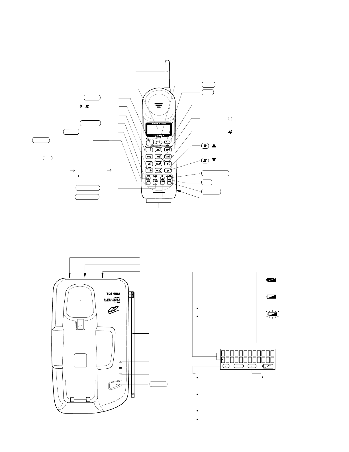
OPERATING CONTROLS
ging
HANDSET CONTROLS
Antenna
Liquid Crystal Display (LCD)
TALK button
0-9, , Dial buttons
TONE button
PAUSE button
MEM (Memory)button
FUNC (Function) button
Press to enter the Function Mode to
perform various settings. Each time
FUNC
the button is pressed, the
menu changes in the following order:
DIAL MEMORY AREA CODE
CIDCW ON/OFF AUTO TALK
ON/OFF.
DELETE button
CANCEL button
BASE UNIT CONTROLS
Char
contacts
RDL (Redial) button
CID (Caller ID) button
Press to enter the caller ID mode.
Number 1 button
Used for long distance dialing.
Number 8 ( ) button (time button)
Used to display the date and time of the received calls.
Number 9 ( ) button
Used to display the number of calls attempted by a caller
( ) button (up arrow button)
Used to scroll up the display screen.
( ) button (down arrow button)
Used to scroll down the display screen.
VOL/RING button
CH (Channel) button
FLASH button
Battery compartment
.
Cradle
PAGE
IN USE
CHARGE
POWER
LINE modular jack
DC IN 9V jack
Tone/Pulse switch
Base antenna
IN USE LED
CHARGE LED
POWER LED
PAGE button
Dot matrix display
Twelve digits by two lines dot
matrix LCD. Shows the time, caller
ID, memory location, instructions,
error messages, and other
information.
The back light of the LCD operates
in the following manner:
Turns on during an incoming call
when the ringer is OFF.
Turns on for 5 seconds and then
off
-when a button is pressed (except
in battery low status).
-when the phone rings and the
handset is lifted from its cradle on
the base unit to answer a call.
talk call id mem
talk icon
Blinks
-while the handset is connecting
to the base unit.
-when a channel is being changed.
Displayed during a call in progress
on the handset.
call id icon
Blinks when the handset is
connecting to the base unit.
Displayed during the caller ID
review mode.
Battery icon
Displayed while the handset is being
charged.
Displayed while the handset is being
charged during the battery low stat us.
Blinks when the battery low s tatus
occurs during standby and phone
conversation.
mem icon
Displayed
-while data is being stored in and
deleted from memory.
-while the Function Mode is in
use.
— 2 —
Page 4

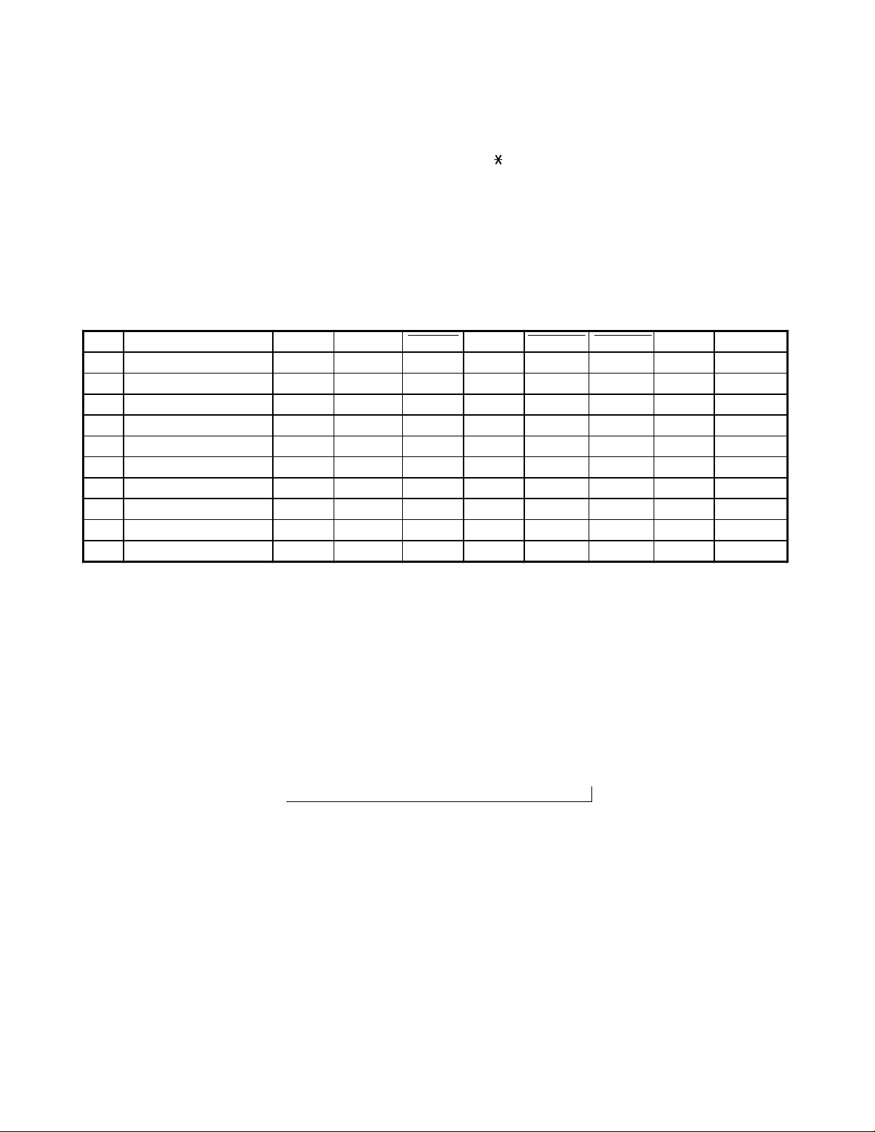
ALIGNMENT PROCEDURE
Test Mode For Base Unit
To change the unit to TEST mode, set the TONE/PULSE switch to PULSE position and press the PAGE key
continuously for 2 seconds while resetting by turning the power on.
When entered the TEST mode, the CHARGE LED turns off, the IN USE LED will light and the unit enters TEST
mode 1.
1. Rotation: Press PAGE key when the “TONE/PULSE” switch is set to Pulse.
2. To change channel: Press PAGE key when the “TONE/PULSE” switch is set to Tone.
( Note: The channel returns to the start channel when changing the step.)
3. To cancel TEST mode: BELL IN, CHG ON, POWER OFF
Note: CHARGE LED lights for about 50 msec when changing the step and channel each time by pressing the
PAGE key.
STEP FUNCTION START CH TX PWR TX MUTE RX MUTE RL CNT REMARKS
1 VCO/TX FREQ. ADJ 19 L L L L
2 TX MOD. CHEC K 19 L H L H
3TX DATA 19 L L L L
4 RX SENS 19 H L H H
5 SQ SENS 19 L L *A H
6 SINGLE TONE 19 H L L H
7 DUAL TONE 19 H L L H
8 DATA IN CHECK 19 L L L L
9 CHARGE CHECK 19 H L L L
10 DUPLEX 19 L H H H
*
1
*
2
*
3
*
4
*
5
*A : Squelch ON: H (CHARGE LED ON) Squelch OFF: L (CHARGE LED OFF)
*1 : In TEST mode 3, “0000...” is output continuously as transmitting data.
*2 : In TEST mode 6, ROW1 → 2 → 3 → 4 → COL1 → 2 → 3 → ROW1 → ... is output in the order when CHGIN
starts up at CHGCNT=H.
*3 : In TEST mode 7, increment of 1 → 2 → 3 → 4 → ...0 →
→ # is performed in the order when CHGIN starts up
at CHGCNT=H.
*4 : In TEST mode 8, CHARGE LED lights when the data received is “0000 ...”.
*5 : In TEST mode 9, DATA “1” is output continuously from CHGCNT, and CHARGE LED lights when CHGIN is “L”.
Channel rotation
19 → 20 → 40 → 1 → 2 → 3 → 4 → 5. . . . . . . . . 37 → 38 → 39 → 40
→
— 3 —
Page 5
Test Mode For Handset Unit
To perform the TEST mode, turn the power ON by pressing the “ ” and “#” buttons at the same time.
When entered the TEST mode, the bell rings and the unit enters TEST mode 1 . ( Refer to the following table. )
1. To change the TEST mode: Press the number key for the corresponding TEST mode.
(Refer to the following table)
2. To change channel: Press “CHANNEL” key.
( Note: If the step is changed, the channel returns to the start channel. )
3. To cancel the TEST mode: Turn the power OFF, charge the Handset, press the “TALK” key.
STEP FUNCTION KEY START CH TX PWR RL PWR TX MUTE RX MUTE CONV REMARKS
1 VCO/TX FREQ. ADJ 1 21 L H L L H
2 TX MOD. CHECK 2 21 L H H L L
3TX DATA 3 21 L H L L L
4 RX SENS 4 21 H H L H L
5 SQ SENS 5 21 L H L *A L
6 RECEIVE DATA CHECK 6 21 L H L L H
7 BELL 7 21 H L L L H
8 BATTERY LOW CHECK 8 21 H L L L H
9 CHARGE CHECK 9 21 H L L L H
10 DUPLEX 0 21 L H H H L
*
1
*
2
*
3
*
4
*
5
*A : Squelch ON: H Squelch OFF: L
*1 : In TEST mode 3, “0000...” is output continuously as transmitting data.
*2 : In TEST mode 6, bell (1kHz) rings lowly when the data received is “0000...”.
*3 : In TEST mode 7, bell rings loudly with initial 2 tone (2kHz, 2.2kHz).
*4 : In TEST mode 8, bell (1kHz) rings lowly when P BATLOW is “L”.
*5 : In TEST mode 9, bell rings lowly when P CHRGIN is “L”.
Channel rotation
21 → 20 → 19 → 40 → 1 → 2 → 3 → 4 → 5 . . . . . . . 37 → 38 → 39 → 40
→
— 4 —
Page 6
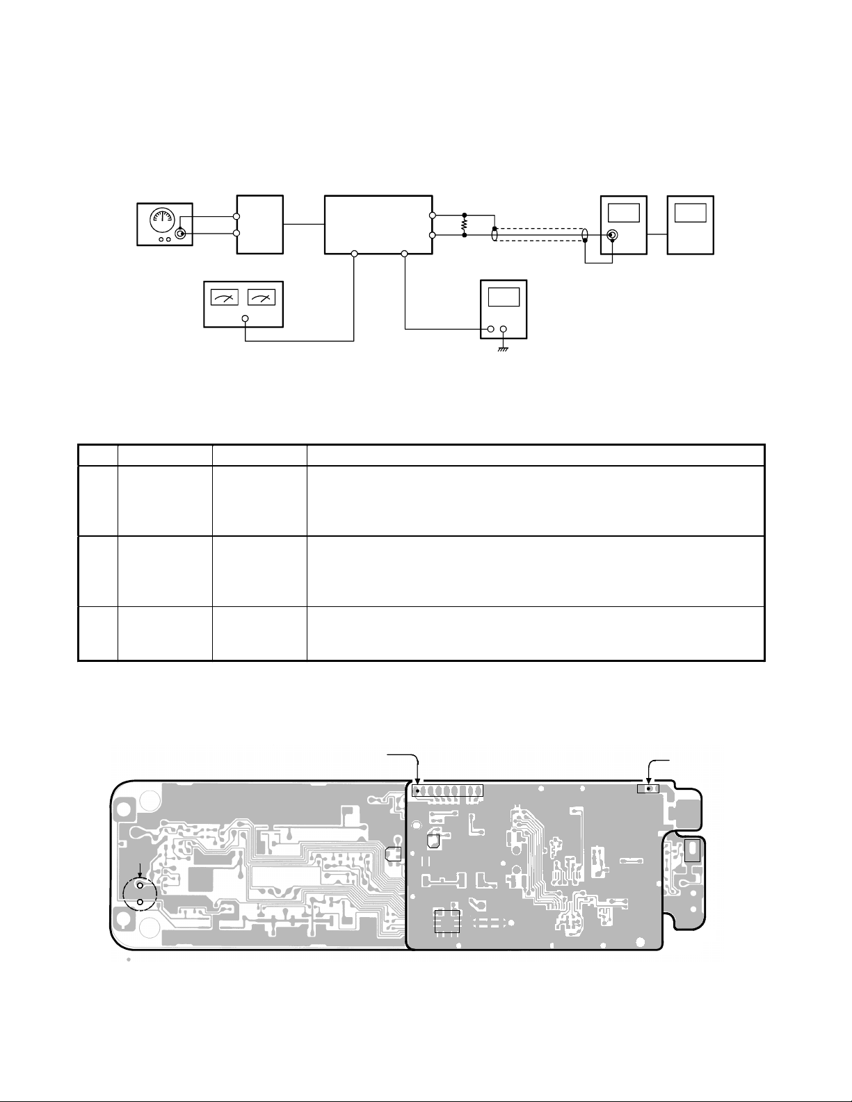
Base Unit
Transmitter Section
Connection
Power
Meter
Frequency
Counter
Deviation
Meter
RF
Test Poi nt
RF
Test Poi nt
BASE RF PCB
RF
Test Poi nt
BASE MAIN PCB
J2
DC IN
9V Jack
TEL Line
J3
Jack
DC 9V
AF GEN.
1kHz 45mV
AC
Adapter
Preset
Place the Base unit in VCO/TX FREQ. ADJ mode in accordance with the procedure on page 3.
Alignment Procedure
Step Adjustment Remarks
1
2
3
VR202
(TX Power)
CT201
(TX Frequency)
RT2
(TX Modulation)
Connect the Power Meter to the RF test point on the Base RF PCB. Adjust
VR202 for a −6.5 dBm reading on the Power Meter.
Connect the Frequency Counter to the RF test point on the Base RF PCB.
Adjust CT201 to make sure that the frequency is 926.893873 MHz.
Press the “PAGE” key to enter the TEST Mode 2. Connect the AF Generator
to the TEL Line Jack on the Base Main PCB. Make sure that the output is 1
kHz 78 mV from the AF Generator.
Connect the Deviation Meter to the RF test point on the Base RF PCB.
Adjust RT2 to indicate ±8 kHz Dev.
AC 120V
60Hz
Alignment Point Location on Base Main PCB and Base RF PCB
Base Main PCB
Base RF PCB
RT2
CT201
VR202
J201
J3
TEL LINE Jack
J2
DC IN 9V Jack
T
S2
T/P Switch
P
RF TEST POINT
Page 7
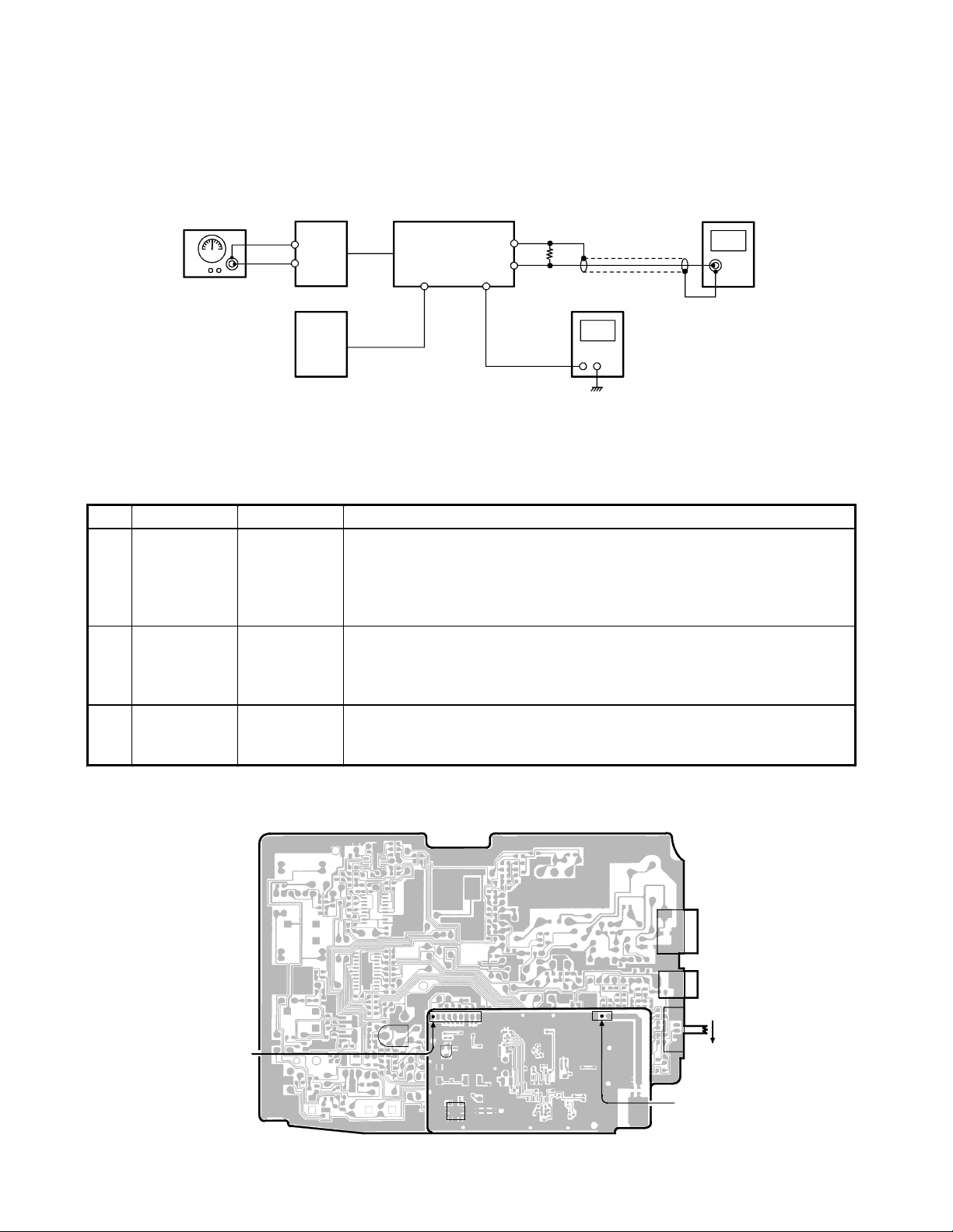
Receiver Section
Connection
RF SG
AC 120V
60Hz
BASE RF PCB
-
RF
+
Test Point
AC Adapter
DC 9V
BASE MAIN PCB
J2
DC IN
9V Jack
TEL Line
J3
-
Jack
+
J1
AF Terminal
Dummy Load
(600-ohm)
DC Voltmeter
AC Voltmeter
Preset
Place the Base unit in VCO/TX FREQ. ADJ mode in accordance with the procedure on page 3.
Alignment Procedure
Step Preset to Adjustment Remarks
Press the “PAGE” key for 3 times to enter the TEST Mode 4. Connect the
1
SG: 1mV
No modulation
SG: 1 mV
2
1 kHz ±8kHz
deviation
SG: −6.5 dBµV
3
No modulation
L212
(Discriminator
Voltage)
RT1
(RX AF
Voltage)
VR201
(SQ Point)
RF Signal Generator to the RF test point on the Base RF PCB. Make sure
that the frequency is 902.984676 MHz.
Connect the DC Voltmeter to the J1 AF test point. Adjust L212 to indicate
DC 0.85 V.
Connect the RF Signal Generator to the RF test point on the Base RF
PCB. Make sure that the frequency is 902.984676 MHz.
Connect the AC Voltmeter across a 600-ohm dummy to the Telephone
Line Jack. Adjust RT1 for a 195 mV reading on the AC voltmeter.
Press the “PAGE” key to enter the TEST Mode 5. Make sure that the
frequency of RF SG output is 902.984676 MHz. Adjust VR201 to turn to
the point where the CHG LED just turns on.
Alignment Point Location on Handset Main PCB and Handset RF PCB
Base Main PCB
AF TEST POINT
RT1
Base RF PCB
J202
VR201
L212
J201
J3
TEL LINE Jack
J2
DC IN 9V Jack
T
S2
T/P Switch
P
RF TEST POINT
Page 8

Handset Unit
Transmitter Section
Connection
Power
Meter
Frequency
Counter
Deviation
Meter
RF
Test Point
RF
Test Point
HANDSET RF PCB
RF
Test Point
HANDSET MAIN PCB
Battery
Terminals
MIC + Pin
DC 3.8V
AF GEN.
1kHz 10.5mV
DC Power Supply
Preset
Place the Handset in VCO/TX FREQ. ADJ mode in accordance with the procedure on page 4.
Alignment Procedure
Step Adjustment Remarks
1
2
3
VR502
(TX Power)
CT501
(TX Frequency )
VR601
(TX Modulation)
Connect the RF power Meter to the RF tes t point on the handset RF P CB .
Adjust VR502 for a −7 dBm reading on the Power Met er .
Connect the Frequency Counter to the RF tes t point on the handset RF
PCB. Adjust CT 501 to make sure that the frequency is 903.085147 MHz .
Press the “2” k ey to enter the TEST M ode 2. Connect the AF G ener ator to
the MIC Connector. Make sure that the output is 1 kHz 10.5 mV from the AF
Generator.
Connect the Deviation Met er to the RF test point on the handset RF PCB.
Adjust VR601 to indicat e ± 8kHz Dev.
Alignment Point Location on Handset Main PCB and Handset RF PCB
Handset Main PCB
MIC + Pin
MC601
RF PCB
VR601
CT501
RF TEST POINT
J501
VR502
Page 9
Receiver Section
Connection
RF SG
HANDSET RF PCB
-
RF
Test Point
+
DC Power Supply
DC 3.8V
HANDSET MAIN PCB
J602
Battery
Terminals
Connector
J601
AF Terminal
SP
Dummy Load
(150-ohm)
+
DC Voltmeter
AC Voltmeter
Preset
Place the Handset in RX SENS mode (step 4) in accordance with the procedure on page 4.
Alignment Procedure
Step Preset to Adjustment Remarks
Connect the RF Signal Generator to the RF test point on the handset RF
PCB. Make sure that the frequency is 926.994344 MHz.
Connect the DC Voltmeter to the J601 AF test point. Adjust L512 to
indicate DC 0.95 V.
Connect the RF Signal Generator to the RF test point on the handset RF
PCB. Make sure that the frequency is 926.994344 MHz.
Connect the AC Voltmeter across a 150-ohm dummy to the SP
Connector. Adjust VR602 for a 65 mV reading on the AC Voltmeter.
Press the “5” key to enter the TEST Mode 5. Make sure that the frequency
of RF SG output is 926.994344 MHz. Adjust VR501 to turn to the point
where there is no signal on the oscilloscope.
SG: 1 mV
1
No modulation
SG: 1 mV
2
1 kHz ±8 kHz
deviation
SG: −6.5 dBµV
3
1 kHz ±8 kHz
deviation
L512
(Discriminator
Voltage)
VR602
(RX AF
Output)
VR501
(SQ Point)
Oscilloscope
Alignment Point Location on Handset Main PCB and Handset RF PCB
AF TEST POINT
Handset Main PCB
VR602
MIC + Pin
MC601
RF PCB
J502
VR501
L512
RF TEST POINT
J501
J602
SP
Connector
Page 10
Base, Main
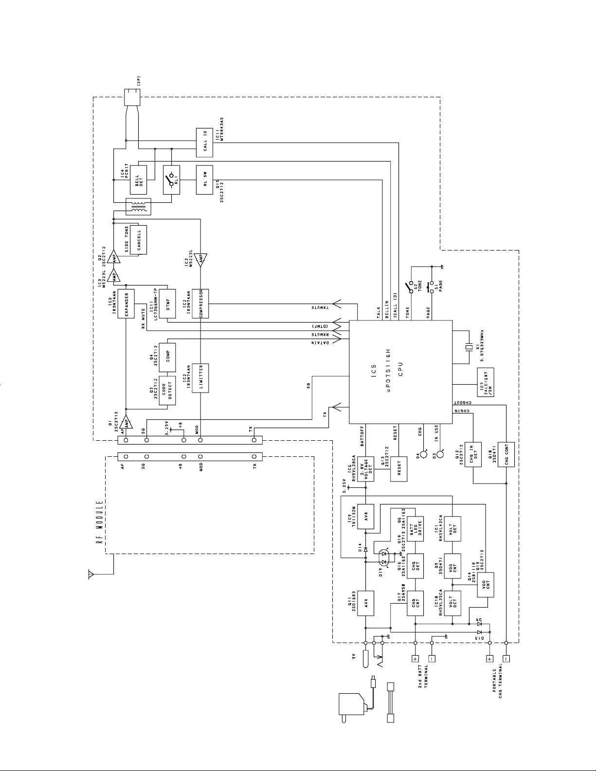
BLOCK DIAGRAMS
— 9 —
Page 11

Base, RF
— 10 —
Page 12

Handset, Main
— 11 —
Page 13

Handset, RF
— 12 —
Page 14

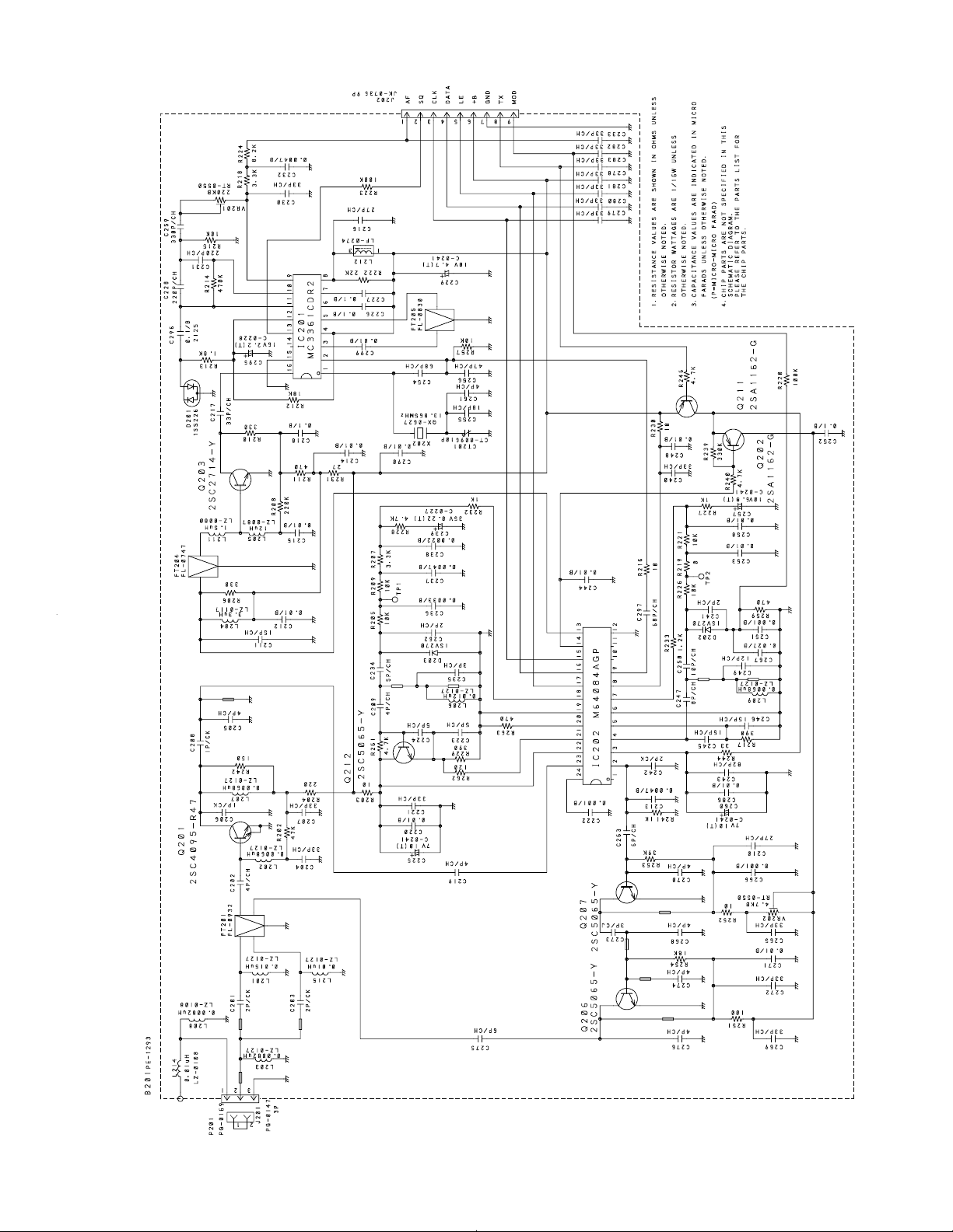
SCHEMATIC DIAGRAMS
Base, Main
— 13 — —14 —
Page 15
Base, RF
— 15 — —16 —
Page 16
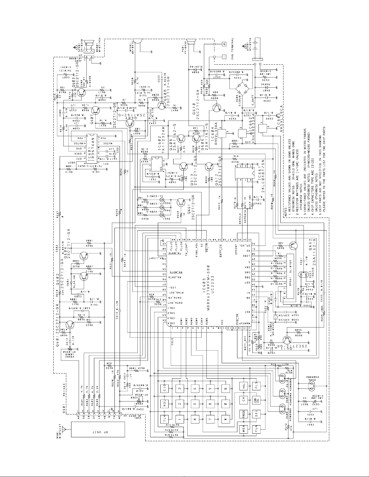
Handset, Main
— 17 — —18 —
Page 17

Handset, RF
— 19 — —20 —
Page 18
TROUBLESHOOTING HINTS
1. The bell does not ring.
When the PAGE SW of the
base is pressed, does the
ringer on the handset ring?
OK
When the TEL SG is joined
with the base to make bell
signal, is there pulse wave
at Pin 4 of IC4 ?
OK
Is there pulse wave at
pin 59 of IC5?
OK
Check IC5 and its
peripheral circuit.
NG
NG
NG
See 2. The bell does not
ring & page does not ring.
Check IC4 and TEL network
circuit.
Check R62, R65 and C41.
Deletion of the Caller ID memory
To delete the Caller ID memory in the EEPROM, proceed with the following process:
1) Set the TONE/PULSE switch to TONE position.
2) While pressing the PAGE button, plug the AC power adapter into the base. Keep pressing the PAGE button for more
than 2 seconds. CHARGE LED will blink rapidly.
Page 19
2. The bell does not ring & page does not ring.
Can the base and handset
be connected?
OK
Press handset DIAL key
while in TALK MODE.
Can key touch sound be
heard from the ring?
OK
When the PAGE SW S1 of
the base is pressed, does
pin19 of IC5 change from
high to low?
NG
NG
NG
See 3. The base and
handset cannot be
connected.
When the key of the
handset is pressed, can the
pulse output at pin 58 of
IC603 be seen?
OK
At the Q606 collector, can
the pulse wave be seen?
OK
Check RINGER Y601.
Check R40, R42 and S1.
NG
NG
Check IC603.
Check R627,R629,R667,
Q605,Q606, and Q613.
Check IC5 and its
peripheral circuit.
Page 20

3. The base and handset cannot be connected.
Check whether the base is
able to set in the test
mode 1.
OK
Check the TX POWER and
the TX FREQUENCY on
the base unit.
OK
Set the base in the test
mode 3, check whether
deviation of the TX data is
app. 7 kHz Dev.
OK
Set the base in the test
mode 8, 902.984676 MHz
(250 Hz ±7 kHz Dev.) 1 mV
output sig nal from RF jack
is applied.
Can the INUSE LED be
lighted?
OK
NG
NG
NG
NG
Check IC5 and its
peripheral circuit.
Check base RF unit.
Check whether there is a
250 Hz data waveform at
pin 9 of J1.
OK
Check base RF unit.
Check whether there is a
250 Hz data waveform at
pin 1 of J1.
OK
Check whether there is a
250 Hz data waveform at
the Q1 collector.
NG
NG
NG
Check RT2, R30, R31, R32
R33, R57 and C28.
Check base RF unit.
Check RT1, Q1 and their
peripheral circuits.
Check whether the
handset is able to set in the
test mode 1.
OK
Check the TX POWER and
the TX FREQUENCY on
the handset unit.
OK
NG
NG
OK
Check whether there is a
250 Hz data waveform at
pin 37 of IC5.
OK
Check IC5 and its
peripheral circuit.
Check IC603 and its
peripheral circuit.
Check handset RF unit.
NG
Check Q3, Q4 and their
peripheral circuits.
Page 21
Set the handset in the test
mode 3, check whether
deviation of the TX data is
app. 7 kHz Dev.
OK
NG
Check whether there is a
250Hz data waveform at
pin 9 of J601.
OK
Check handset RF unit.
NG
Check VR601, R619, R632,
R634, R635, R636
and C611.
Set the handset in the test
mode 6, 926.994344 MHz
(250 Hz ±7 kHz Dev.) 1mV
output signal from RF jack
is applied. Check whether
the bell ring.
OK
Place the handset on the
base to charge about
5 seconds, then connect
again.
NG
Check whether the 250 Hz
data wareform from pin 1
of J601 is fed.
OK
Check whether there is a
250 Hz data waveform at
the Q601 collector.
OK
Check whether there is a
250 Hz data waveform at
pin 55 of IC603.
OK
Check IC603 and its
peripheral circuit.
NG
NG
NG
Check handset RF unit.
Check VR602, Q601 and
their peripheral circuits .
Check Q602, Q604 and
their peripheral circuits .
Page 22

4. Cannot make a phone call (pulse).
Can the base and handset
be connected?
OK
While in TALK MODE,
press dial key of the
handset.
Check whether squar e
waveform from pin 58 of
IC5 is fed.
OK
Check Q15, RL1 and their
peripheral circuits.
NG
NG
See 3. The base and
handset cannot be
connected.
Check IC5.
5. Cannot make a phone call (tone).
Can the base and handset
be connected?
OK
While in TALK MODE,
press dial key of the
handset. Can tone
waveform from pin20 of
IC11 is fed?
OK
Can tone signal be heard
from the handset speaker?
OK
Check the base TEL-line
circuit and RELAY control
circuit.
NG
NG
NG
See 3. The base and
handset be cannot be
connected.
Check IC11 and
its peripheral circuits.
Check IC3, Q2 and their
peripheral circuits.
Page 23

6. Voice cannot be transmitted to other party (outgoing call).
Can the base and handset
be connected?
OK
The 1 kHz, 12.5 mV sine
waveform is applied to
MC601 side, can the
1 kHz sine waveform from
pin 7 of IC601 be fed?
OK
Check whether there is the
1 kHz sine waveform at
pin 10 of IC601.
OK
Check whether there is the
1 kHz sine waveform at
pin 9 of 601.
OK
TX output signal from the
handset is detected by the
liner detecter, can the 1 kHz
sine waveform be fed?
NG
NG
NG
NG
NG
See 3. The base and
handset cannot be
connected.
Check Q608 and its
peripheral circuit.
Check IC601 and its
peripheral circuit.
Check VR601 and its
peripheral circuit.
Check handset RF unit.
OK
Check whether there is the
1 kHz sine waveform at
pin 1 of J1 on the base unit.
OK
Check whether there is the
1 kHz sine waveform at
pin 5 of IC2.
OK
Check whether there is the
1 kHz sine waveform at
pin 3 of IC2.
OK
Check whether there is the
1 kHz sine waveform at the
Q2 collector.
OK
Check whether the 1 kHz
sine waveform from
TEL-line output is fed.
OK
NG
NG
NG
NG
NG
Check base RF unit.
Check RT1, Q1 and their
peripheral circuits.
Check IC2 and its
peripheral circuit.
Check IC3, Q2 and their
peripheral circuits.
Check T1, RL1 and their
peripheral circuits.
Check MC601 of handset.
Page 24

7. The voice of the caller cannot be heard (incoming call).
Can the base and handset
be connec ted?
OK
The 1 kHz 77.5 mV sine
waveform is applied to
TEL-line of the base, can the
1 kHz sine waveform from
the Q2 collector be fed?
OK
Check whether there is the
1 kHz sine waveform at
pin 7 of IC2.
OK
Check whether there is the
1 kHz sine waveform at
pin 10 of IC2.
OK
Check whether there is the
1 kHz sine waveform at
pin 9 of J1.
OK
TX output signal from the
base is detected by the
liner detector, can the 1 kHz
sine waveform be fed?
OK
Check whether there is the
1 kHz sine waveform at
pin 1 of J601 on the
handset unit.
OK
Check whether there is the
1 kHz sine waveform at
pin 5 of IC601.
OK
Check whether there is the
1 kHz sine waveform at the
pin 3 of IC601.
OK
Check whether there is the
1 kHz sine waveform at
pin 1 of J602.
OK
NG
NG
NG
NG
NG
NG
NG
NG
NG
NG
See 3. The base and
handset cannot be
connected.
Check the base TEL-line
circuit and RELAY control
circuit.
Check IC3 and its
peripheral circuit.
Check IC2 and its
peripheral circuit.
Check RT2 and its
peripheral circuit.
Check base RF unit.
Check handset RF unit.
Check VR602, Q601 and
hteir peripheral circuits .
Check IC601 and its
peripheral circuit.
Check Q603 and its
peripheral circuit.
Check SP801 and WA801.
Page 25

IC AND TRANSISTOR VOLTAGE CHART
C
B
E
C
B
E
C
B
E
C
B
E
C
B
E
C
B
E
C
B
E
C
B
E
C
B
E
C
B
E
C
B
E
C
B
E
C
B
E
C
B
E
C
B
E
C
B
E
Q17
Q18
Q19
Q20
Transistors Unit [V]
Ref.
Pin STBY TALK Note
No.
1.0/3.0 1.8
Q1
Q2
Q3
Q4
Q5
Q6
Q7
Q8
Q9
Q10
Q11
Q12
Q13
Q14
Q15
Q16
0.6/0.8 0.7
00
3.4 3.4
1.3 1.3
0.6 0.6
0/1.0 1/1.0
0.6 0.6
00
0/3.2 0/3.2
0/0.6 0/0.6
00
0 1.6
2.7 1.0
1.7 1.7
00
4.2 4.2
4.2 4.2
00
3.2 3.2
3.2 3.2
0 3.2
3.0 2.5
3.2 3.2
0 3.2
3.0 2.5
3.2 3.2
0.1 0.1
00
00
8.3 7.7
5.4 5.4
4.8 5.5
3.2 3.2
00
00
2.6 2.6
00
00
4.2 4.2
8.0 8.0
8.0 8.0
4.2 0
0 0.7
00
00
8.8 8.8
9.0 9.0
Ref.
Pin STBY TALK Note
No.
C 8.6 8.6
B 8.0 8.0
E 8.6 8.6
C 4.2 4.2
B0 0
E0 0
C 8.0 8.0
B0 0
E0 0
C0 0
B 0.8 0.8
E0 0
C0 0
Q201 B 0.8 0
E0 0
C0 0
Q202 B0 0
E0 0
C 2.2 2.2
Q203 B 0.7 0.7
E0 0
C0 0
Q206 B0 0
E0 0
C0 0
Q207 B0 0
E0 0
C 0 3.0
Q211 B 3.0 2.5
E 3.0 3.0
C 2.6 2.6
Q212 B 2.4 2.4
E 1.8 1.8
C 0 2.4
Q501 B 0 0.8
E0 0
C 0 3.0
Q502 B 0 2.3
E 0 3.2
C 0 2.1
Q503 B 0 0.7
E0 0
C 0 2.0
Q506 B 0 0.8
E0 0
C 0 0.9
Q507 B 0 0.7
E0 0
Unit [V]
— 28 —
Page 26

Ref.
C
B
E
C
B
E
C
B
E
C
B
E
C
B
E
C
B
E
C
B
E
C
B
E
C
B
E
C
B
E
C
B
E
C
B
E
C
B
E
C
B
E
C
B
E
IC1
IC2
IC3
IC4
IC5
Pin STBY TALK Note
No.
C 0 3.0
Q511 B 0 2.4
E 0 3.2
C 0 2.5
Q512 B 0 2.4
E 0 1.7
0/2.4 1.8
Q601
Q602
Q603
Q604
Q605
Q606
Q607
Q608
Q609
Q610
Q611
Q612
Q613
Q661
Q662
0/0.8 0.7
00
0/0.7 0/0.8
0/0.5 0.5
00
0 1.4
0 1.0
0 0.2
0/3.2 0/3.2
0/0.6 0/0.6
00
00
3.2 3.2
3.8 3.8
00
00
00
00
0 0.6
00
0 1.6
0 0.8
0 0.2
0 3.0
0/3.2 2.4
0/3.2 3.2
3.1 3.2
00
00
2.8/3.0 2.8
00
00
00
0/3.2 0
00
3.2 3.2
00
00
2.4 2.4
00
00
0 3.2
2.8/3.0 2.5
3.2 3.2
Unit [V]
IC'S Unit [V]
Ref.
Pin STBY TALK Note
No.
1 4.8 4.8
2 5.0 5.0
30 0
1 3.0 3.2
2 0 2.3
3 0 1.2
40 0
5 0.5/2.0 1.2
6 1.3 1.3
7 1.3 1.3
8 1.3 1.3
9 0.6 0.6
10 1.3 1.2
11 0 2.3
12 0 0
1 1.6 1.6
2 1.6 1.6
3 1.6 1.6
40 0
5 1.6 1.6
6 1.6 1.6
7 1.6 1.6
8 4.2 4.2
10 0
20 0
30 0
4 3.1 3.1
10 0
20 0
30 0
40 0
50 0
60 0
70 0
8 3.2 3.2
90 0
10 0 0
11 0 0
12 0 0
13 0 0
14 0 0
15 0 0
16 0 0
17 0 0
18 3.2 3.2
19 0 3.2
20 0 2.7
21 0 2.7
22 2.3 2.2
23 2.8 0.2
24 0 0
25 0 0
— 29 —
Page 27

Ref.
26
27
28
29
30
31
32
33
34
35
36
37
38
39
40
41
42
43
44
45
46
47
48
49
50
51
52
53
54
55
56
57
58
59
60
61
62
63
64
1
2
3
1
2
3
4
5
6
7
8
IC8
IC9
IC10
IC11
Pin STBY TALK Note
No.
00
00
2.8 2.8
2.8 2.8
2.8 0.2
2.8 0.2
00
00
00
1.0 1.0
3.2 3.2
0/3.2 0/3.2
3.2 0
00
3.0 3.0
3.0 3.0
0/2.8 0
0/2.8 2.8
0/2.8 2.8
IC5
IC6
IC7
00
2.8 0
2.8 2.8
00
00
00
00
0 2.8
2.8 2.8
2.8 2.8
0.4/2.6 0.4/2.6 SINE WAVE
0/2.6 0/2.6 SINE WAVE
00
0 2.5
3.0 3.2
2.8 2.8
2.8 2.8
00
00
00
3.2 3.2
3.2 3.2
00
00
00
00
00
3.2 2.7
0 2.7
00
2.7 3.2
Unit [V]
Ref.
Pin STBY TALK Note
No.
1 1.7 1.7
2 1.7 1.7
3 1.7 1.7
4 1.7 1.7
5 1.7 1.7
60 0
70 0
80 0
90 0
10 0.6/2.6 0.6/2.6
11 0.3/3.0 0.3/3.0
12 0 0
13 0 0
14 0 0
15 0 0
16 3.2 3.2
17 3.2 3.2
18 3.2 3.2
19 3.2 3.2
20 0 0
21 0 0
22 0 0
23 0 0
24 3.2 3.2
1 4.1 4.1
20 0
3 1.3 1.3
4 3.2 3.2
50 0
6 4.1 4.1
1 7.1 7.3
2 7.9 8.2
30 0
1 3.2 3.2
2 1.2 1.2
30 0
4 2.7 2.7
5 2.7 2.7
60 0
70 0
80 0
9 0.3/2.3 0.3/2.3
10 0 0.2/3.2
11 0 0
12 3.2 3.2
13 0 0
14 0 0
15 0 0
16 2.8 2.8
17 2.8 2.8
18 0 0
19 0 0
Unit [V]
— 30 —
Page 28

Ref.
20
IC601
IC602
IC603
Pin STBY TALK Note
No.
IC11
1 3.2 3.2
2 2.8 2.8
3 2.6 2.6
4 3.2 3.2
5 2.8 2.8
6 2.8 2.8
7 2.8 2.8
IC201 8 3.2 3.2
9 0.9 1.0
10 0.6 0.6
11 0.7 0.7
12 0.6 0.6
13 3.1 3.1
14 0 0
15 0 0
16 0 3.2
10 0
20 0
30 0
40 0
50 0
60 0
7 0 0.8
8 3.1 3.1
9 3.1 3.1
10 2.6 1.0
11 1.7 1.7
IC202
IC501
12 0 0
13 3.1 3.1
14 0 0
15 0 0.1
16 3.0 3.0
17 0 2.9
18 0 1.6
19 0 0
20 1.0 1.1
21 1.8 0.7
22 2.6 2.5
23 1.6 2.4
24 1.6 1.6
1 0 2.5
2 0 2.4
3 0 2.6
4 0 3.2
5 0 2.7
6 0 2.7
7 0 2.7
8 0 3.2
9 0 1.5
10 0 0.6
1.2 1.2
Unit [V]
Ref.
No.
IC501
IC502
Unit [V]
Pin STBY TALK Note
11 0 0.7
12 0 0.6
13 0 3.1
14 0 0
15 0 0
16 0 3.2
10 0
2 0 1.6
3 0 2.7
4 0 2.6
5 0 1.8
60 0
70 0
8 0 3.0
9 0 3.0
10 0 2.6
11 0 1.7
12 0 0
13 0 3.1
14 0 0
15 0 0
16 0 3.1
17 0 3.2
18 0 1.0
19 0 0
20 0 1.0
21 0 1.7
22 0 2.5
23 0 1.6
24 0 2.4
1 0 3.0
2 0 2.3
3 0 1.2
4 0 0.6
5 0 1.0/1.4
6 0 1.2
70 0
80 0
9 0 0.6
10 0 1.0/1.4
11 0 0
12 0 0
1 0 2.7
20 0
3 0 1.2
4 0/3.2 3.2
50 0
6 3.8 3.8
1 3.2 3.2
20 0
30 0
— 31 —
Page 29

Ref.
4
5
6
7
8
9
10
11
12
13
14
15
16
17
18
19
20
21
22
23
24
25
26
27
28
29
30
31
32
33
34
35
36
37
38
39
40
41
42
43
44
45
46
47
48
49
50
51
IC603
IC604
IC605
IC661
IC662
Pin STBY TALK Note
No.
00
00
00
0/3.2 0
00
00
00
2.8/3.0 2.8
00
00
3.2 3.2
3.2 3.2
3.2 3.2
0.8/2.8 2.8
00
2.8/3.0 2.8
00
00
0/2.4 0/2.4 SINE WAVE
0/3.0 0/3.0 SINE WAVE
00
00
00
IC603
00
00
00
00
00
00
0/2.8 2.8
0/2.8 2.8
0/2.8 2.8
00
00
3.2 3.2
00
00
00
0 2.8
00
00
0/2.8 0
0/2.8 0
0/2.8 2.8
0/2.8 2.8
00
00
00
Unit [V]
Ref.
Pin STBY TALK Note
No.
52 0 0
53 0 0
54 0 2.6
55 0/3.2 0/3.2
56 2.8/3.0 2.8
57 0 0/2.8
58 0 0
59 0 0
60 0/1.0 1.1
61 3.2 3.2
62 0 3.2
63 3.2 3.2
64 0 3.2
1 3.2 3.2
2 3.8 3.8
30 0
1 3.2 3.2
2 3.2 3.2
30 0
10 0
20 0
30 0
40 0
5 0/2.8 2.8
6 0/2.8 2.8
70 0
8 0/3.2 3.2
10 0
2 3.8 3.8
3 3.2 3.2
Unit [V]
— 32 —
Page 30

Base Unit
SEMICONDUCTOR LEAD IDENTIFICATION
D1: HZ33-2
D2/D5/D7/D8/D9/D11/D12/D17/D18: 1N4148
D13/D14: 1N4003
D20: HZ6A2
Cathode
D15: HSM88WA
Anode1, 2
Cathode1 Cathode2
Anode
D16: HZK6C
Cathode
D3: LTL-16 KG E
D4: LTL-16 KP E
D19:VRPG3312X
Anode
Anode
(Green)
Cathode
Anode
Anode (Red)
Cathode
D10: RLS4148
Cathode
D201: 1SS226
Anode/Cathode
Anode Cathode
Anode
D202/D203: 1SV270
Cathode
Q10: 2SD471
E
C
B
Anode
Q1/Q2/Q3/Q4/Q12/Q13/Q15/Q18/Q19/Q20:
2SC2712
Q203: 2SC2714
Q5/Q6/Q7/Q8/Q9/Q16/Q20 2/Q 211 : 2SA116 2
Q206/Q207/Q212: 2SC5065
C
B: Base
E: Emitter
BE
E
C
B
C: Collector
Q17: 2SA950
C
B
B: Base
E: Emitter
C: Collector
E
Q14: 2SB1118
B
C E
Q201: 2SC4095
BE
EC
B: Base
E: Emitter
C: Collector
Page 31

IC1
RH5VL42CA
IC6
RH5VL28CA
IC10
RH5VL35CA
IC2
IR3N74AN
Vcc
MUTE
EO
EREC
EPI
VREF
IC3
M5223L
GND
1
2
3
4
5
6
12
11
10
MUTE
CO
CREC
9
ACP
8
CPI
7
8
IC4
PC817
1
2
4
3
IC5
µ
PD75116
3
2
1
V
64 63 62 61 60 59 58 57 56 55 54 53 52
1
2
3
4
5
6
7
8
9
10
11
12
13
14
15
16
17
18
19
20 21 22 23 24 25 26 27 28 29 30 31 32
1
Vcc
WP
SDA
IC8
MT88E43
Vin
6
5
Vout
1
2
3
4
5
6
7
8
9
10
11
12
24
23
22
21
20
19
18
17
16
15
14
13
IC7
24LC16BT/SN
1
A0
51
50
49
48
47
46
45
44
43
42
41
40
39
38
37
36
35
34
33
IC9
TK11232AM
NOISE BYPASS
2
A1
3
A2 SCL
Vss
4
CONT
1
GND
2
34
8
7
6
5
IC11
LC7366NM
DD
1
V
2
XMIT
3
C1
4
5
C2
6
C3
Vss
7
8
9
OSCI
10
OSCO
20
TONE OUT
19
CD
18
R1
17
16
R2
15
R3
R4
14
13
12
MUTE
11
C4
IC201
MC3361CDR2
Osc.
Mixer
Output
Vcc
Limiter
Input
Quad
Input
1
2
3
4
5
6
7
8
Crystal
Decoupling
Mixer
16
Input
15
GND
Audio
14
Mute
Scan
13
Control
Squelch
12
Input
Filter
11
Output
Filter
10
Input
Demodulator
9
Audio
IC202
M64084AGP
NC
124
Tx OUT
Tx GND
223
322
Tx Vcc
421
TxB
520
TxE
619
PD1
718
817
Vcc
916
Xin
Xout
10 15
11 14
XBo
GND
12 13
MIX REF
MIX IN
Rx Vcc
RxB
RxE
Rx GND
PD2
RST
SI
CPS
Lock
MIX OUT
Page 32

Handset
e
D501/D667: 1SS226
Anode/Cathode
Anode Cathode
D605: S1ZB20
−
~
D502/D503: 1SV270
Cathode
Anode
D606/D608/D609/D610: HSM88WA
+
~
Anode1, 2
Cathode1 Cathode2
D601/D604: RLS4148
Cathode
D607: HZK6C
Cathode
Anod
Anode
D661/D662/D663: CL-220G
Cathode
Anode
Q501: 2SC4095
BE
EC
Q503: 2SC2714
Q601/Q602/Q603/Q604/Q607/Q608/Q610/Q611/Q612/Q613/Q661: 2SC2712
Q502/Q511/Q605/Q606/Q609/Q662: 2SA1162
Q506/Q507/Q512: 2SC5065
C
B: Base
E: Emitter
C: Collector
BE
Page 33

IC501
MC3361CDR2
IC603
MB89627RPFM
Crystal
Osc.
Mixer
Output
Vcc
Limiter
Input
Decoupling
Quad
Input
IC502
M64084AGP
NC
Tx OUT
Tx Vcc
TxB
TxE
Tx GND
PD1
Vcc
Xin
Xout
10 15
11 14
XBo
GND
12 13
1
2
3
4
5
6
7
8
124
223
322
421
520
619
718
817
916
Mixer
16
Input
GND
15
Audio
14
Mute
Scan
13
Control
Squelch
12
Input
Filter
11
Output
Filter
10
Input
Demodulator
9
Audio
MIX REF
MIX IN
Rx Vcc
RxB
RxE
Rx GND
PD2
RST
SI
CPS
Lock
MIX OUT
IC601
IR3N74AN
MUTE
EREC
Vcc
EO
EPI
VREF
GND
1
2
3
4
5
6
12
11
10
MUTE
CO
CREC
9
ACP
8
CPI
7
IC602
TK11232AM
CONT
GND
NOISE BYPASS
1
2
34
Vin
6
5
Vout
IC605
RH5VL28CA
IC604
RH5VL33AA
IC662
RH5RE32AA
IC661
24LC04BT/SN
1
A0
2
A1
A2
3
Vss
4
3
2
1
8
Vcc
7
WP
6
SCL
5
SDA
Page 34

Base, Main
ELECTRICAL PARTS LOCATION
— 37 —
Page 35

Base, RF
— 38 —
Page 36

Handset, Main
— 39 —
Page 37

Handset, RF
— 40 —
Page 38

Handset
WIRING DIAGRAM
— 41 —
Page 39

EXPLODED VIEW AND MECHANICAL PARTS LIST
Base, Unit
31
16
10
17
4
24
23
25
30
28
15
5
22
22
18
22
26
32
33
1
27
22
6
8
2
3
24
7
Note:
To remove the RF Assembly from the unit, remove four screws
Three screws
23
are used for fastening the Shield Cases 26 and 27 .
24
24
29
.
Page 40

Base Unit
LOC.
NO.
10 RC005526 GCAS456906Z Hook for FT-8808 ABS 1
15 RC008041 PLBS458999Z Label, ID for FT-8808 1
16 RC005180 PLBZ456717Z Label, Indication for FT-8808 1
17 RC008026 PLBZ458780Z Label, Indication 1
18 RC008855 GCAS458578Z LED Lens PMMA 1
22 RC000941 SSCW802608N Screw, P Tight Bind HD + D2.6X8 NI 9
23 RC004893 SSCW802612N Screw, P Tight Bind HD + D2.6X12 NI 3
24 RC004028 SSCW802616N Screw, P Tight Bind HD + D2.6X16 NI 8
25 RC001752 SSCW283012N Screw, Tapping Bind+& SP Washer D3X12 NI 1
26 RC008768 GSDC258035Z Shield Case ABS 1
27 RC008769 GSDC258036Z Shield Case ABS 1
28 RC005691 NSPZ457885Z Spring Terminal SWP 2
29 RC008871 GCAS458918Z Stand for FT-8808 ABS 1
30 RC005692 NSPZ457886Z Torsion Spring SWP 1
31 RC005696 RUTC457032Z Wool Coated Paper, Wool Tack 2
32 RC008770 HSDC458037Z Shield Case SPTE 1
33 RC008771 HSDC458038Z Shield Case SPTE 1
PART NO. REF. NO. DESCRIPTION QTY
1 RC008040 GNBZ458919Z Button, Push for FT-8808 ABS 1
RC008856 GNBZ458579Z Button, Push for FT-8808BK ABS
2 RC008897 GCAS458497Z Case, Battery for FT-8808 ABS 1
RC005680 GCAS257882Z Case, Battery for FT-8808BK ABS
3 RC008039 GCAS258917Z Case, Bottom for FT-8808 ABS 1
RC008853 GCAS158576Z Case, Bottom for FT-8808BK ABS
4 RC008038 GCAS258916Z Case, Top for FT-8808 ABS 1
RC008852 GCAS158575Z Case, Top for FT-8808BK ABS
5 RC005686 HTML457884Z Charge Terminal C5191(PBP) 2
6 RC004860 HTML451849Z Contact Plate C5191(PBP) 1
7 RC002384 LFUT428079Z Foot Bumpon SJ-5916 1.6T 4
8 RC008851 GHDZ458580Z Holder, LED ABS 1
RC005684 GCAS457909Z Hook for FT-8808BK ABS
RC008025 PLBS458779Z Label, ID for FT-8808BK
RC005329 PLBZ456718Z Label, Indication for FT-8808BK
RC008854 GCAS358577Z Stand for FT-8808BK ABS
— 43 —
Page 41

Handset
58
67
64
72
73
67
56
67
59
68
69
63
70
77
55
51
74
71
67
52
61
75
53
65
66
Note:
To remove the RF Assembly from the unit, remove four screws
Three screws
68
are used for fastening the Shield Cases 70 and 71 .
78
76
69
62
60
54
57
.
Page 42

Handset
LOC.
NO.
51 RC008915 RBLD458506Z Blind for FT-8808 PC 1
52 RC008044 GNBZ458923Z Button, Function for FT-8808 ABS 1
53 RC008912 GNBZ458504Z Button, Push for FT-8808 ABS 1
54 RC008042 GCAS358921Z Case, Front for FT-8808 ABS 1
55 RC008907 GCAS358499Z Case, Rear for FT-8808 ABS 1
56 RC008707 HTML457893Z Charge Terminal C2680(BSP) 2
57 RC008909 GCAS458501Z Cover for FT-8808 Elastomer 1
58 RC008908 GCAS458500Z Cover, Battery for FT-8808 ABS 1
59 RC008715 RCUM417955Z Cushion Moltplene 1
60 RC004286 RCUN451209Z Cushion Neoprene 1
61 RC008709 LHDZ456969Z Holder, MIC EPDM 1
62 RC008043 GHDZ458922Z Holder, Speaker for FT-8808 ABS 1
63 RC008710 LNBZ357895Z Key Rubber SI 1
64 RC008713 PLBZ458086Z Label, Caution 1
65 RC008046 PLBS459000Z Label, ID for FT-8808 1
66 RC008045 KDPZ458924Z Plate, Display for FT-8808 PMMA 1
67 RC000941 SSCW802608N Screw, P Tight Bind HD + D2.6X8 NI 8
68 RC004893 SSCW802612N Screw, P Tight Bind HD + D2.6X12 NI 3
69 RC004028 SSCW802616N Screw, P Tight Bind HD + D2.6X16 NI 4
70 RC008768 GSDC258035Z Shield Case ABS 1
71 RC008769 GSDC258036Z Shield Case ABS 1
72 RC008711 NSPZ457894Z Spring Terminal SWP 2
73 RC008770 HSDC458037Z Shield Case SPTE 1
74 RC008771 HSDC458038Z Shield Case SPTE 1
75 RC008868 RCUN458729Z Cushion Neoprene 1
76 RC008864 GHDZ354112Z Holder, Display PC 1
77 RC008033 RZEB458984Z Insulation Plate 1
78 RC008032 RETC454528Z Reflection Sheet 1
PART NO. REF. NO. DESCRIPTION QTY
RC008714 RBLD457881Z Blind for FT-8808BK PVC
RC008705 GNBZ357892Z Button, Function for FT-8808BK ABS
RC008706 GNBZ457891Z Button, Push for FT-8808BK ABS
RC008865 GCAS358653Z Case, Front for FT-8808BK ABS
RC008701 GCAS157888Z Case, Rear for FT-8808BK ABS
RC008703 GCAS457897Z Cover for FT-8808BK Elastomer
RC008702 GCAS357889Z Cover, Battery for FT-8808BK ABS
RC008866 GHDZ458654Z Holder, Speaker for FT-8808BK ABS
RC008031 PLBS458781Z Label, ID for FT-8808BK
RC008867 KDPZ458655Z Plate, Display for FT-8808BK PMMA
— 45 —
Page 43

PARTS LIST
PRODUCT SAFETY NOTE: Products marked with a have special characteristics important to safety.
Before replacing any of these components, read carefully the product safety notice of this service manual.
Don’t degrade the safety of the product through important servicing.
Symbol
%
LOC.
NO.
CAPACIT ORS
The following codes indicate variation of capacitors against temperatures,:
YA = ±5%, YB = ±10%, YD = +20 −30%, YE = +20 −50% (−25 ~ +85 °C), ZF = +30 −80%, (−10 ~ +79 °C),
CH = 0 ±60 ppm/°C, TH = −470 ppm/°C, ±60 ppm/°C, B = ±10%, F = +30 −80%,
SL = +350 ppm/°C ~ −1000 ppm/°C, UJ = −750 ppm/°C ±120 ppm/°C, CJ = 0 ± 120 ppm/°C, CK = 0 ± 250 ppm/°C
C1 RC002229 BCXT511045Z CERAMIC 0.1UF 25V K B
C2 RC003983 BCBH816804Z CERAMIC 68PF 50V J CH
C3 RC002229 BCXT511045Z CERAMIC 0.1UF 25V K B
C4 RC001069 BCXT811035Z CERAMIC 0.01UF 50V K B
C5 RC002849 BCXK512240Z CERAMIC 0.22UF 25V Z F
C6 RC002229 BCXT511045Z CERAMIC 0.1UF 25V K B
C7 RC001631 BCXT812235Z CERAMIC 0.022UF 50V K B
C14 RC004947 BCAP314706Z ELECTROLYTIC 47UF 16V M C-130
C15 RC004952 BCAP811096Z ELECTROLYTIC 1UF 50V M C-130
C16 RC002229 BCXT511045Z CERAMIC 0.1UF 25V K B
C17 RC004952 BCAP811096Z ELECTROLYTIC 1UF 50V M C-130
C18 RC001825 BCXT816825Z CERAMIC 0.0068UF 50V K B
C19 RC005101 BCAP112216Z ELECTROLYTIC 220UF 10V M C-130
C20 RC001069 BCXT811035Z CERAMIC 0.01UF 50V K B
C21 RC003976 BCBH811014Z CERAMIC 100PF 50V J CH
C22 RC002229 BCXT511045Z CERAMIC 0.1UF 25V K B
C23 RC000777 BCZY0120001 SEMI-CONDUCTOR 0.022UF 18V
C24 RC004945 BCAP111016Z ELECTROLYTIC 100UF 10V M C-130
C25 RC002233 BCXT814725Z CERAMIC 0.0047UF 50V K B
C26 RC008020 BCZY0260001 MYLAR 0.56UF 250V K
C27 RC004172 BCXT813925Z CERAMIC 0.0039UF 50V K B
C28 RC002224 BCXK811040Z CERAMIC 0.1UF 50V Z F
C29 RC001068 BCXT811025Z CERAMIC 0.001UF 50V K B
C31 RC002229 BCXT511045Z CERAMIC 0.1UF 25V K B
C032 RC004421 BCXT812725Z CERAMIC 0.0027UF 50V K B
C033 RC003970 BCBH815604Z CERAMIC 56PF 50V J CH
C034 RC004951 BCAP811006Z ELECTROLYTIC 10UF 50V M C-130
C35 RC002594 BCXT516835Z CERAMIC 0.068UF 25V K B
C36 RC003291 BCXT813935Z CERAMIC 0.039UF 50V K B
C37 RC000752 BCKB821025Z CERAMIC 0.001UF 500V K YB(B)
C38 RC005512 BCKB131025Z CERAMIC 0.001UF 1000V K YB(B)
C39 RC001068 BCXT811025Z CERAMIC 0.001UF 50V K B
C40 RC008048 BCAP903316Z ELECTROLYTIC 330UF 6.3V M C-130
F
±1
PART NO.
G
±2
J
±5
REF
NO.
K
±10
M
±20
N
±30
Z
−20+80P0+100
DESCRIPTION
Symbol
pF
C
±0.25
D
±0.5
— 46 —
Page 44

LOC.
NO.
PART NO.
REF
NO.
DESCRIPTION
C41 RC001632 BCXT813335Z CERAMIC 0.033UF 50V K B
C43 RC001068 BCXT811025Z CERAMIC 0.001UF 50V K B
C44 RC002224 BCXK811040Z CERAMIC 0.1UF 50V Z F
C45 RC004008 BCBH813314Z CERAMIC 330PF 50V J CH
C46 RC002849 BCXK512240Z CERAMIC 0.22UF 25V Z F
C47 RC002849 BCXK512240Z CERAMIC 0.22UF 25V Z F
C48 RC005512 BCKB131025Z CERAMIC 0.001UF 1000V K YB(B)
C49 RC000777 BCZY0120001 SEMI-CONDUCTOR 0.022UF 18V
C50 RC001068 BCXT811025Z CERAMIC 0.001UF 50V K B
C51 RC001069 BCXT811035Z CERAMIC 0.01UF 50V K B
C52 RC001068 BCXT811025Z CERAMIC 0.001UF 50V K B
C53 RC002229 BCXT511045Z CERAMIC 0.1UF 25V K B
C54 RC002229 BCXT511045Z CERAMIC 0.1UF 25V K B
C55 RC004508 BCXC311050Z CERAMIC 1UF 16V Z F
C56 RC004945 BCAP111016Z ELECTROLYTIC 100UF 10V M C-130
C57 RC004945 BCAP111016Z ELECTROLYTIC 100UF 10V M C-130
C58 RC003979 BCBH812704Z CERAMIC 27PF 50V J CH
C59 RC003979 BCBH812704Z CERAMIC 27PF 50V J CH
C60 RC001068 BCXT811025Z CERAMIC 0.001UF 50V K B
C61 RC001069 BCXT811035Z CERAMIC 0.01UF 50V K B
C62 RC001069 BCXT811035Z CERAMIC 0.01UF 50V K B
C63 RC001069 BCXT811035Z CERAMIC 0.01UF 50V K B
C64 RC001069 BCXT811035Z CERAMIC 0.01UF 50V K B
C65 RC002224 BCXK811040Z CERAMIC 0.1UF 50V Z F
C66 RC002229 BCXT511045Z CERAMIC 0.1UF 25V K B
C67 RC001068 BCXT811025Z CERAMIC 0.001UF 50V K B
C68 RC005161 BCAP311016Z ELECTROLYTIC 100UF 16V M C-130
C69 RC001069 BCXT811035Z CERAMIC 0.01UF 50V K B
C70 RC004951 BCAP811006Z ELECTROLYTIC 10UF 50V M C-130
C71 RC001631 BCXT812235Z CERAMIC 0.022UF 50V K B
C72 RC002229 BCXT511045Z CERAMIC 0.1UF 25V K B
C73 RC004945 BCAP111016Z ELECTROLYTIC 100UF 10V M C-130
C74 RC001069 BCXT811035Z CERAMIC 0.01UF 50V K B
C75 RC001068 BCXT811025Z CERAMIC 0.001UF 50V K B
C201 RC005223 BCMS812091Z CERAMIC 2PF 50V C CK
C202 RC005218 BCMM814091Z CERAMIC 4PF 50V C CH
C203 RC005223 BCMS812091Z CERAMIC 2PF 50V C CK
C204 RC005216 BCMM813304Z CERAMIC 33PF 50V J CH
C205 RC005218 BCMM814091Z CERAMIC 4PF 50V C CH
C206 RC005222 BCMS811091Z CERAMIC 1PF 50V C CK
C207 RC005216 BCMM813304Z CERAMIC 33PF 50V J CH
C208 RC005222 BCMS811091Z CERAMIC 1PF 50V C CK
C209 RC008785 BCMM814098Z CERAMIC 4PF 50V B CH
C210 RC005215 BCMM812704Z CERAMIC 27PF 50V J CH
C211 RC005212 BCMM811504Z CERAMIC 15PF 50V J CH
C212 RC005205 BCML811035Z CERAMIC 0.01UF 50V K B
— 47 —
Page 45

LOC.
NO.
PART NO.
REF
NO.
DESCRIPTION
C213 RC005208 BCML814725Z CERAMIC 0.0047UF 50V K B
C214 RC005205 BCML811035Z CERAMIC 0.01UF 50V K B
C215 RC005205 BCML811035Z CERAMIC 0.01UF 50V K B
C216 RC005215 BCMM812704Z CERAMIC 27PF 50V J CH
C217 RC005216 BCMM813304Z CERAMIC 33PF 50V J CH
C218 RC005202 BCML311045Z CERAMIC 0.1UF 16V K B
C219 RC005218 BCMM814091Z CERAMIC 4PF 50V C CH
C220 RC005205 BCML811035Z CERAMIC 0.01UF 50V K B
C221 RC005216 BCMM813304Z CERAMIC 33PF 50V J CH
C222 RC005204 BCML811025Z CERAMIC 0.001UF 50V K B
C223 RC008755 BCMM815098Z CERAMIC 5PF 50V B CH
C224 RC008755 BCMM815098Z CERAMIC 5PF 50V B CH
C225 RC004185 BCSS951006Z TANTALUM CHIP 10UF 7V M A C-241
C226 RC005202 BCML311045Z CERAMIC 0.1UF 16V K B
C227 RC005202 BCML311045Z CERAMIC 0.1UF 16V K B
C228 RC005214 BCMM812214Z CERAMIC 220PF 50V J CH
C229 RC005225 BCSS114796Z TANTALUM CHIP 4.7UF 10V M A C-241
C230 RC005216 BCMM813304Z CERAMIC 33PF 50V J CH
C231 RC005214 BCMM812214Z CERAMIC 220PF 50V J CH
C232 RC005208 BCML814725Z CERAMIC 0.0047UF 50V K B
C233 RC005216 BCMM813304Z CERAMIC 33PF 50V J CH
C234 RC008755 BCMM815098Z CERAMIC 5PF 50V B CH
C235 RC008754 BCMM813098Z CERAMIC 3PF 50V B CH
C236 RC005207 BCML813325Z CERAMIC 0.0033UF 50V K B
C237 RC005208 BCML814725Z CERAMIC 0.0047UF 50V K B
C238 RC005206 BCML812225Z CERAMIC 0.0022UF 50V K B
C239 RC004446 BCPP662286Z TANTALUM CHIP 0.22UF 35V M A C-227
C240 RC005216 BCMM813304Z CERAMIC 33PF 50V J CH
C241 RC008753 BCMM812098Z CERAMIC 2PF 50V B CH
C242 RC005223 BCMS812091Z CERAMIC 2PF 50V C CK
C243 RC008757 BCMM818204Z CERAMIC 82PF 50V J CH
C244 RC005205 BCML811035Z CERAMIC 0.01UF 50V K B
C245 RC005212 BCMM811504Z CERAMIC 15PF 50V J CH
C246 RC005212 BCMM811504Z CERAMIC 15PF 50V J CH
C247 RC005221 BCMM818092Z CERAMIC 8PF 50V D CH
C248 RC005205 BCML811035Z CERAMIC 0.01UF 50V K B
C249 RC005211 BCMM811204Z CERAMIC 12PF 50V J CH
C250 RC005209 BCMM811002Z CERAMIC 10PF 50V D CH
C251 RC005204 BCML811025Z CERAMIC 0.001UF 50V K B
C252 RC005202 BCML311045Z CERAMIC 0.1UF 16V K B
C253 RC005205 BCML811035Z CERAMIC 0.01UF 50V K B
C254 RC005220 BCMM816804Z CERAMIC 68PF 50V J CH
C255 RC005213 BCMM811804Z CERAMIC 18PF 50V J CH
C256 RC005219 BCMM814704Z CERAMIC 47PF 50V J CH
C257 RC008758 BCSS116896Z TANTALUM CHIP 6.8UF 10V M A C-241
C258 RC005205 BCML811035Z CERAMIC 0.01UF 50V K B
— 48 —
Page 46

LOC.
NO.
PART NO.
REF
NO.
DESCRIPTION
C259 RC005217 BCMM813314Z CERAMIC 330PF 50V J CH
C260 RC004185 BCSS951006Z TANTALUM CHIP 10UF 7V M A C-241
C261 RC005218 BCMM814091Z CERAMIC 4PF 50V C CH
C262 RC008753 BCMM812098Z CERAMIC 2PF 50V B CH
C263 RC005360 BCMM816092Z CERAMIC 6PF 50V D CH
C265 RC005216 BCMM813304Z CERAMIC 33PF 50V J CH
C266 RC005204 BCML811025Z CERAMIC 0.001UF 50V K B
C267 RC008752 BCML512735Z CERAMIC 0.027UF 25V K B
C268 RC005218 BCMM814091Z CERAMIC 4PF 50V C CH
C269 RC005216 BCMM813304Z CERAMIC 33PF 50V J CH
C270 RC005218 BCMM814091Z CERAMIC 4PF 50V C CH
C271 RC005205 BCML811035Z CERAMIC 0.01UF 50V K B
C272 RC005216 BCMM813304Z CERAMIC 33PF 50V J CH
C273 RC005224 BCMT813091Z CERAMIC 3PF 50V C CJ
C274 RC005218 BCMM814091Z CERAMIC 4PF 50V C CH
C275 RC005360 BCMM816092Z CERAMIC 6PF 50V D CH
C276 RC005218 BCMM814091Z CERAMIC 4PF 50V C CH
C278 RC005216 BCMM813304Z CERAMIC 33PF 50V J CH
C279 RC005216 BCMM813304Z CERAMIC 33PF 50V J CH
C280 RC005216 BCMM813304Z CERAMIC 33PF 50V J CH
C281 RC005216 BCMM813304Z CERAMIC 33PF 50V J CH
C282 RC005216 BCMM813304Z CERAMIC 33PF 50V J CH
C283 RC005216 BCMM813304Z CERAMIC 33PF 50V J CH
C286 RC005205 BCML811035Z CERAMIC 0.01UF 50V K B
C290 RC005205 BCML811035Z CERAMIC 0.01UF 50V K B
C295 RC003287 BCPT312296Z TANTALUM CHIP 2.2UF 16V M A C-228
C296 RC002229 BCXT511045Z CERAMIC 0.1UF 25V K B
C297 RC005220 BCMM816804Z CERAMIC 68PF 50V J CH
C299 RC005205 BCML811035Z CERAMIC 0.01UF 50V K B
C501 RC005224 BCMT813091Z CERAMIC 3PF 50V C CJ
C502 RC005289 BCMM815091Z CERAMIC 5PF 50V C CH
C503 RC005224 BCMT813091Z CERAMIC 3PF 50V C CJ
C504 RC005210 BCMM811014Z CERAMIC 100PF 50V J CH
C505 RC005218 BCMM814091Z CERAMIC 4PF 50V C CH
C506 RC005290 BCMS815081Z CERAMIC 0.5PF 50V C CK
C507 RC005216 BCMM813304Z CERAMIC 33PF 50V J CH
C508 RC005222 BCMS811091Z CERAMIC 1PF 50V C CK
C509 RC008755 BCMM815098Z CERAMIC 5PF 50V B CH
C510 RC005216 BCMM813304Z CERAMIC 33PF 50V J CH
C511 RC005212 BCMM811504Z CERAMIC 15PF 50V J CH
C512 RC005205 BCML811035Z CERAMIC 0.01UF 50V K B
C513 RC005205 BCML811035Z CERAMIC 0.01UF 50V K B
C514 RC005205 BCML811035Z CERAMIC 0.01UF 50V K B
C515 RC005205 BCML811035Z CERAMIC 0.01UF 50V K B
C516 RC005215 BCMM812704Z CERAMIC 27PF 50V J CH
C517 RC005216 BCMM813304Z CERAMIC 33PF 50V J CH
— 49 —
Page 47

LOC.
NO.
PART NO.
REF
NO.
DESCRIPTION
C518 RC005202 BCML311045Z CERAMIC 0.1UF 16V K B
C519 RC005223 BCMS812091Z CERAMIC 2PF 50V C CK
C520 RC005205 BCML811035Z CERAMIC 0.01UF 50V K B
C521 RC005216 BCMM813304Z CERAMIC 33PF 50V J CH
C522 RC005204 BCML811025Z CERAMIC 0.001UF 50V K B
C523 RC008755 BCMM815098Z CERAMIC 5PF 50V B CH
C524 RC008755 BCMM815098Z CERAMIC 5PF 50V B CH
C525 RC004185 BCSS951006Z TANTALUM CHIP 10UF 7V M A C-241
C526 RC005202 BCML311045Z CERAMIC 0.1UF 16V K B
C527 RC005202 BCML311045Z CERAMIC 0.1UF 16V K B
C528 RC005214 BCMM812214Z CERAMIC 220PF 50V J CH
C529 RC005225 BCSS114796Z TANTALUM CHIP 4.7UF 10V M A C-241
C530 RC005216 BCMM813304Z CERAMIC 33PF 50V J CH
C531 RC005214 BCMM812214Z CERAMIC 220PF 50V J CH
C532 RC005208 BCML814725Z CERAMIC 0.0047UF 50V K B
C533 RC005216 BCMM813304Z CERAMIC 33PF 50V J CH
C534 RC008785 BCMM814098Z CERAMIC 4PF 50V B CH
C535 RC008755 BCMM815098Z CERAMIC 5PF 50V B CH
C536 RC005207 BCML813325Z CERAMIC 0.0033UF 50V K B
C537 RC005208 BCML814725Z CERAMIC 0.0047UF 50V K B
C538 RC005206 BCML812225Z CERAMIC 0.0022UF 50V K B
C539 RC004446 BCPP662286Z TANTALUM CHIP 0.22UF 35V M A C-227
C540 RC005216 BCMM813304Z CERAMIC 33PF 50V J CH
C541 RC008755 BCMM815098Z CERAMIC 5PF 50V B CH
C542 RC005223 BCMS812091Z CERAMIC 2PF 50V C CK
C543 RC008757 BCMM818204Z CERAMIC 82PF 50V J CH
C544 RC005205 BCML811035Z CERAMIC 0.01UF 50V K B
C545 RC005212 BCMM811504Z CERAMIC 15PF 50V J CH
C546 RC005212 BCMM811504Z CERAMIC 15PF 50V J CH
C547 RC008756 BCMM816091Z CERAMIC 6PF 50V C CH
C548 RC005205 BCML811035Z CERAMIC 0.01UF 50V K B
C549 RC008755 BCMM815098Z CERAMIC 5PF 50V B CH
C550 RC005212 BCMM811504Z CERAMIC 15PF 50V J CH
C551 RC005204 BCML811025Z CERAMIC 0.001UF 50V K B
C552 RC005202 BCML311045Z CERAMIC 0.1UF 16V K B
C553 RC005205 BCML811035Z CERAMIC 0.01UF 50V K B
C554 RC005220 BCMM816804Z CERAMIC 68PF 50V J CH
C555 RC005213 BCMM811804Z CERAMIC 18PF 50V J CH
C556 RC005219 BCMM814704Z CERAMIC 47PF 50V J CH
C557 RC008758 BCSS116896Z TANTALUM CHIP 6.8UF 10V M A C-241
C558 RC005205 BCML811035Z CERAMIC 0.01UF 50V K B
C559 RC005217 BCMM813314Z CERAMIC 330PF 50V J CH
C560 RC004185 BCSS951006Z TANTALUM CHIP 10UF 7V M A C-241
C561 RC005218 BCMM814091Z CERAMIC 4PF 50V C CH
C562 RC005290 BCMS815081Z CERAMIC 0.5PF 50V C CK
C563 RC005360 BCMM816092Z CERAMIC 6PF 50V D CH
— 50 —
Page 48

LOC.
NO.
PART NO.
REF
NO.
DESCRIPTION
C565 RC005216 BCMM813304Z CERAMIC 33PF 50V J CH
C566 RC005204 BCML811025Z CERAMIC 0.001UF 50V K B
C567 RC008752 BCML512735Z CERAMIC 0.027UF 25V K B
C568 RC005218 BCMM814091Z CERAMIC 4PF 50V C CH
C569 RC005216 BCMM813304Z CERAMIC 33PF 50V J CH
C570 RC005218 BCMM814091Z CERAMIC 4PF 50V C CH
C571 RC005205 BCML811035Z CERAMIC 0.01UF 50V K B
C572 RC005216 BCMM813304Z CERAMIC 33PF 50V J CH
C573 RC005224 BCMT813091Z CERAMIC 3PF 50V C CJ
C574 RC005218 BCMM814091Z CERAMIC 4PF 50V C CH
C575 RC005360 BCMM816092Z CERAMIC 6PF 50V D CH
C576 RC005218 BCMM814091Z CERAMIC 4PF 50V C CH
C578 RC005216 BCMM813304Z CERAMIC 33PF 50V J CH
C579 RC005216 BCMM813304Z CERAMIC 33PF 50V J CH
C580 RC005216 BCMM813304Z CERAMIC 33PF 50V J CH
C581 RC005216 BCMM813304Z CERAMIC 33PF 50V J CH
C582 RC005216 BCMM813304Z CERAMIC 33PF 50V J CH
C583 RC005216 BCMM813304Z CERAMIC 33PF 50V J CH
C585 RC004410 BCBH814091Z CERAMIC 4PF 50V C CH
C586 RC005205 BCML811035Z CERAMIC 0.01UF 50V K B
C590 RC005205 BCML811035Z CERAMIC 0.01UF 50V K B
C595 RC003287 BCPT312296Z TANTALUM CHIP 2.2UF 16V M A C-228
C596 RC002229 BCXT511045Z CERAMIC 0.1UF 25V K B
C597 RC005220 BCMM816804Z CERAMIC 68PF 50V J CH
C599 RC005205 BCML811035Z CERAMIC 0.01UF 50V K B
C601 RC003291 BCXT813935Z CERAMIC 0.039UF 50V K B
C602 RC002234 BCXT814735Z CERAMIC 0.047UF 50V K B
C603 RC002229 BCXT511045Z CERAMIC 0.1UF 25V K B
C604 RC008731 BCXK311050Z CERAMIC 1UF 16V Z F
C605 RC002229 BCXT511045Z CERAMIC 0.1UF 25V K B
C607 RC004185 BCSS951006Z TANTALUM CHIP 10UF 7V M A C-241
C608 RC004903 BCFZ114706Z ELECTROLYTIC 47UF 10V M C-258
C609 RC004448 BCSS956896Z TANTALUM CHIP 6.8UF 7V M A C-241
C610 RC004172 BCXT813925Z CERAMIC 0.0039UF 50V K B
C611 RC008731 BCXK311050Z CERAMIC 1UF 16V Z F
C612 RC002229 BCXT511045Z CERAMIC 0.1UF 25V K B
C613 RC002229 BCXT511045Z CERAMIC 0.1UF 25V K B
C614 RC002229 BCXT511045Z CERAMIC 0.1UF 25V K B
C615 RC004185 BCSS951006Z TANTALUM CHIP 10UF 7V M A C-241
C616 RC004185 BCSS951006Z TANTALUM CHIP 10UF 7V M A C-241
C617 RC002229 BCXT511045Z CERAMIC 0.1UF 25V K B
C618 RC008731 BCXK311050Z CERAMIC 1UF 16V Z F
C619 RC004448 BCSS956896Z TANTALUM CHIP 6.8UF 7V M A C-241
C620 RC001069 BCXT811035Z CERAMIC 0.01UF 50V K B
C621 RC001631 BCXT812235Z CERAMIC 0.022UF 50V K B
C622 RC001631 BCXT812235Z CERAMIC 0.022UF 50V K B
— 51 —
Page 49

LOC.
NO.
PART NO.
REF
NO.
DESCRIPTION
C623 RC002229 BCXT511045Z CERAMIC 0.1UF 25V K B
C624 RC001069 BCXT811035Z CERAMIC 0.01UF 50V K B
C625 RC001069 BCXT811035Z CERAMIC 0.01UF 50V K B
C626 RC001071 BCXT813325Z CERAMIC 0.0033UF 50V K B
C627 RC001071 BCXT813325Z CERAMIC 0.0033UF 50V K B
C628 RC001069 BCXT811035Z CERAMIC 0.01UF 50V K B
C629 RC003968 BCBH812204Z CERAMIC 22PF 50V J CH
C630 RC003968 BCBH812204Z CERAMIC 22PF 50V J CH
C631 RC008731 BCXK311050Z CERAMIC 1UF 16V Z F
C632 RC004902 BCFZ111016Z ELECTROLYTIC 100UF 10V M C-258
C633 RC001069 BCXT811035Z CERAMIC 0.01UF 50V K B
C634 RC001069 BCXT811035Z CERAMIC 0.01UF 50V K B
C635 RC004902 BCFZ111016Z ELECTROLYTIC 100UF 10V M C-258
C639 RC008731 BCXK311050Z CERAMIC 1UF 16V Z F
C640 RC001069 BCXT811035Z CERAMIC 0.01UF 50V K B
C641 RC001069 BCXT811035Z CERAMIC 0.01UF 50V K B
C642 RC001068 BCXT811025Z CERAMIC 0.001UF 50V K B
C643 RC002229 BCXT511045Z CERAMIC 0.1UF 25V K B
C644 RC001631 BCXT812235Z CERAMIC 0.022UF 50V K B
C645 RC002229 BCXT511045Z CERAMIC 0.1UF 25V K B
C661 RC002229 BCXT511045Z CERAMIC 0.1UF 25V K B
C662 RC002229 BCXT511045Z CERAMIC 0.1UF 25V K B
C663 RC001069 BCXT811035Z CERAMIC 0.01UF 50V K B
C664 RC002229 BCXT511045Z CERAMIC 0.1UF 25V K B
C665 RC001069 BCXT811035Z CERAMIC 0.01UF 50V K B
C666 RC001069 BCXT811035Z CERAMIC 0.01UF 50V K B
CT201 RC005226 BCTY0096100 TRIMMER CT-096 CTZ3S10A-W1PF55
CT501 RC005226 BCTY0096100 TRIMMER CT-096 CTZ3S10A-W1PF55
DIODES
D001 RC002468 BDAY0492008 ZENER AX TS 26 + HZ33-2 TD
D002 RC002236 BDAY0246003 DIODE AX TS 26 + 1N4148 T-77
D003 RC004190 BDAY0867001 LED LTL16KGE-A
D004 RC004189 BDAY0866001 LED LTL-16KPE-A
D005 RC002236 BDAY0246003 DIODE AX TS 26 + 1N4148 T-77
D007 RC002236 BDAY0246003 DIODE AX TS 26 + 1N4148 T-77
D008 RC002236 BDAY0246003 DIODE AX TS 26 + 1N4148 T-77
D009 RC002236 BDAY0246003 DIODE AX TS 26 + 1N4148 T-77
D010 RC001826 BDAY0433001 DIODE RLS4148 TE11
D011 RC002236 BDAY0246003 DIODE AX TS 26 + 1N4148 T-77
D012 RC002236 BDAY0246003 DIODE AX TS 26 + 1N4148 T-77
D013 RC000781 BDAY0133001 DIODE 1N4003
D014 RC000781 BDAY0133001 DIODE 1N4003
D015 RC002240 BDAY0485001 DIODE HSM88WA TL
D016 RC003195 BDAY0432004 ZENER HZK6C TR
— 52 —
Page 50

LOC.
NO.
PART NO.
REF
NO.
DESCRIPTION
D017 RC002236 BDAY0246003 DIODE AX TS 26+ 1N4148 T-77
D018 RC002236 BDAY0246003 DIODE AX TS 26+ 1N4148 T-77
D019 RC004661 BDAY0920001 LED VRPG3312X
D020 RC008846 BDAY0492018 ZENER AX TS 26 + HZ6A2 TD
D201 RC001635 BDAY0274001 DIODE 1SS226 TE85L
D202 RC008759 BDAY0908001 DIODE 1SV270(TPH3)
D203 RC008759 BDAY0908001 DIODE 1SV270(TPH3)
D501 RC001635 BDAY0274001 DIODE 1SS226 TE85L
D502 RC008759 BDAY0908001 DIODE 1SV270(TPH3)
D503 RC008759 BDAY0908001 DIODE 1SV270(TPH3)
D601 RC001826 BDAY0433001 DIODE RLS4148 TE11
D604 RC001826 BDAY0433001 DIODE RLS4148 TE11
D605 RC004904 BDAY0792001 DIODE BRIDGE S1ZB20-4062
D606 RC002240 BDAY0485001 DIODE HSM88WA TL
D607 RC003195 BDAY0432004 ZENER HZK6C TR
D608 RC002240 BDAY0485001 DIODE HSM88WA TL
D609 RC002240 BDAY0485001 DIODE HSM88WA TL
D610 RC002240 BDAY0485001 DIODE HSM88WA TL
D661 RC008857 BDAY0896001 LED CL-220G-C-TS
D662 RC008857 BDAY0896001 LED CL-220G-C-TS
D663 RC008857 BDAY0896001 LED CL-220G-C-TS
D667 RC001635 BDAY0274001 DIODE 1SS226 TE85L
FILTERS
FT201 RC008762 BFLY0932001 SAW FL-932 TQS-833C-7R
FT204 RC004873 BFLY0747001 CERAMIC FL-747 SFE14.3MA
FT205 RC005231 BFLY0830001 FILTER FL-830 KBF-455RL-30KC
FT501 RC008762 BFLY0932001 SAW FL-932 TQS-833C-7R
FT504 RC004873 BFLY0747001 CERAMIC FL-747 SFE14.3MA
FT505 RC005231 BFLY0830001 FILTER FL-830 KBF-455RL-30KC
IC’S
IC001 RC008848 BDEY3064003 RH5VL42CA-T1
IC002 RC002588 BDEY2207001 IR3N74AN
IC003 RC001086 BDEY0582001 M5223L
IC004 RC000802 BDEY0577001 PC817
IC005 RC008847 BDDY0773001 UC2232 UPD75116-185
IC006 RC005074 BDEY2937003 RH5VL28CA-T1
IC007 RC008799 BDEY3181003 24LC16BT/SN
IC008 RC008809 BDEY3544003 MT88E43ASR
IC009 RC005648 BDEY3414003 TK11232AM TAPE
IC010 RC005647 BDEY2939003 RH5VL35CA-T1
IC011 RC005516 BDEY1058003 LC7366NM-TP-T2
IC201 RC004870 BDEY2768003 MC3361CDR2
IC202 RC008761 BDEY3571003 M64084AGP-601C
— 53 —
Page 51

LOC.
NO.
PART NO.
REF
NO.
DESCRIPTION
IC501 RC004870 BDEY2768003 MC3361CDR2
IC502 RC008761 BDEY3571003 M64084AGP-601C
IC601 RC002588 BDEY2207001 IR3N74AN
IC602 RC005648 BDEY3414003 TK11232AM TAPE
IC603 RC008858 BDDY0774001 UC2233 MB89627RPFM-580
IC604 RC008861 BDEY2989003 RH5VL33AA-T1
IC605 RC005074 BDEY2937003 RH5VL28CA-T1
IC661 RC008860 BDEY2969003 24LC04BT/SN
IC662 RC008859 BDEY2927003 RH5RE32AA-T1
JACKS
J001 RC004854 BJKY0599009 JK-599 IMSA-9110S-09 9P
J002 RC001094 BJKY0234001 JK-234 DJ13-1
J003 RC003586 BJKY0803002 TEL JK-803 A36-006-4910A 2P
J201 RC004886 BPGY0147003 PLUG PG-147 9218B-1-03A-T 3P
J202 RC004875 BJKY0736009 JK-736 9210B-1-09Z386-T
J501 RC004886 BPGY0147003 PLUG PG-147 9218B-1-03A-T 3P
J502 RC004875 BJKY0736009 JK-736 9210B-1-09Z386-T
J601 RC004854 BJKY0599009 JK-599 IMSA-9110S-09 9P
J602 RC002252 BJKY0600002 JK-600 SB20-02WS 2P
COILS
L201 RC005234 BLZY0127157 INDUCTOR LZ-127 0.015UH J TAPE
L202 RC005236 BLZY0127686 INDUCTOR LZ-127 0.0068UH TAPE
L203 RC005237 BLZY0127826 INDUCTOR LZ-127 0.0082UH TAPE
L204 RC004790 BLZY0117339 INDUCTOR LZ-117 3.3UH K TAPE
L205 RC004877 BLZY0087120 INDUCTOR LZ-087 12UH J TAPE
L206 RC008786 BLZY0127127 INDUCTOR LZ-127 0.012UH J TAPE
L207 RC005236 BLZY0127686 INDUCTOR LZ-127 0.0068UH TAPE
L208 RC004882 BLZY0108826 INDUCTOR LZ-108 0.0082UH K TAPE
L209 RC005236 BLZY0127686 INDUCTOR LZ-127 0.0068UH TAPE
L211 RC005232 BLZY0080159 INDUCTOR LZ-080 1.5UH K TAPE
L212 RC004876 BLFY0274001 COIL LF-274 615LN-0124=P3
L214 RC004878 BLZY0108107 INDUCTOR LZ-108 0.01UH K TAPE
L215 RC005233 BLZY0127107 INDUCTOR LZ-127 0.01UH J TAPE
L501 RC005233 BLZY0127107 INDUCTOR LZ-127 0.01UH J TAPE
L502 RC005235 BLZY0127566 INDUCTOR LZ-127 0.0056UH TAPE
L503 RC005237 BLZY0127826 INDUCTOR LZ-127 0.0082UH TAPE
L504 RC004790 BLZY0117339 INDUCTOR LZ-117 3.3UH K TAPE
L505 RC004877 BLZY0087120 INDUCTOR LZ-087 12UH J TAPE
L506 RC008786 BLZY0127127 INDUCTOR LZ-127 0.012UH J TAPE
L507 RC005236 BLZY0127686 INDUCTOR LZ-127 0.0068UH TAPE
L508 RC004878 BLZY0108107 INDUCTOR LZ-108 0.01UH K TAPE
L509 RC005235 BLZY0127566 INDUCTOR LZ-127 0.0056UH TAPE
L511 RC005232 BLZY0080159 INDUCTOR LZ-080 1.5UH K TAPE
— 54 —
Page 52

LOC.
NO.
PART NO.
REF
NO.
DESCRIPTION
L512 RC004876 BLFY0274001 COIL LF-274 615LN-0124=P3
L515 RC005234 BLZY0127157 INDUCTOR LZ-127 0.015UH J TAPE
T001 RC003234 BTFY0265001 TRANSFORMER TF-265 IT -24E-1B(R295403)
TRANSISTORS
Q1 RC001637 BDBC2712303 DB-381 2SC2712-GR TE85L
Q2 RC001637 BDBC2712303 DB-381 2SC2712-GR TE85L
Q3 RC001637 BDBC2712303 DB-381 2SC2712-GR TE85L
Q4 RC001637 BDBC2712303 DB-381 2SC2712-GR TE85L
Q5 RC001081 BDBA1162107 DB-036 2SA1162-G(GR)TE85L
Q6 RC001081 BDBA1162107 DB-036 2SA1162-G(GR)TE85L
Q7 RC001081 BDBA1162107 DB-036 2SA1162-G(GR)TE85L
Q8 RC001081 BDBA1162107 DB-036 2SA1162-G(GR)TE85L
Q9 RC001081 BDBA1162107 DB-036 2SA1162-G(GR)TE85L
Q10 RC003200 BDBD0471111 DB-411 2SD471-L
Q11 RC005642 BDBD1683119 DB-440 2SD1683-T
Q12 RC001637 BDBC2712303 DB-381 2SC2712-GR TE85L
Q13 RC001637 BDBC2712303 DB-381 2SC2712-GR TE85L
Q14 RC005641 BDBB1118119 DB-133 2SB1118-T TD
Q15 RC001637 BDBC2712303 DB-381 2SC2712-GR TE85L
Q16 RC001081 BDBA1162107 DB-036 2SA1162-G(GR)TE85L
Q17 RC005640 BDBA0950124 DB-010 2SA950-Y
Q18 RC001637 BDBC2712303 DB-381 2SC2712-GR TE85L
Q19 RC001637 BDBC2712303 DB-381 2SC2712-GR TE85L
Q20 RC001637 BDBC2712303 DB-381 2SC2712-GR TE85L
Q201 RC004867 BDBC4095672 DB-810 2SC4095-R47 T1
Q202 RC001081 BDBA1162107 DB-036 2SA1162-G(GR)TE85L
Q203 RC002245 BDBC2714124 DB-718 2SC2714-Y TE85L
Q206 RC008760 BDBC5065124 2SC5065-Y(TE85R)
Q207 RC008760 BDBC5065124 2SC5065-Y(TE85R)
Q211 RC001081 BDBA1162107 DB-036 2SA1162-G(GR)TE85L
Q212 RC008760 BDBC5065124 2SC5065-Y(TE85R)
Q501 RC004867 BDBC4095672 DB-810 2SC4095-R47 T1
Q502 RC001081 BDBA1162107 DB-036 2SA1162-G(GR)TE85L
Q503 RC002245 BDBC2714124 DB-718 2SC2714-Y TE85L
Q506 RC008760 BDBC5065124 2SC5065-Y(TE85R)
Q507 RC008760 BDBC5065124 2SC5065-Y(TE85R)
Q511 RC001081 BDBA1162107 DB-036 2SA1162-G(GR)TE85L
Q512 RC008760 BDBC5065124 2SC5065-Y(TE85R)
Q601 RC001637 BDBC2712303 DB-381 2SC2712-GR TE85L
Q602 RC001637 BDBC2712303 DB-381 2SC2712-GR TE85L
Q603 RC001637 BDBC2712303 DB-381 2SC2712-GR TE85L
Q604 RC001637 BDBC2712303 DB-381 2SC2712-GR TE85L
Q605 RC001081 BDBA1162107 DB-036 2SA1162-G(GR)TE85L
Q606 RC001081 BDBA1162107 DB-036 2SA1162-G(GR)TE85L
— 55 —
Page 53

LOC.
NO.
PART NO.
REF
NO.
DESCRIPTION
Q607 RC001637 BDBC2712303 DB-381 2SC2712-GR TE85L
Q608 RC001637 BDBC2712303 DB-381 2SC2712-GR TE85L
Q609 RC001081 BDBA1162107 DB-036 2SA1162-G(GR)TE85L
Q610 RC001637 BDBC2712303 DB-381 2SC2712-GR TE85L
Q611 RC001637 BDBC2712303 DB-381 2SC2712-GR TE85L
Q612 RC001637 BDBC2712303 DB-381 2SC2712-GR TE85L
Q613 RC001637 BDBC2712303 DB-381 2SC2712-GR TE85L
Q661 RC001637 BDBC2712303 DB-381 2SC2712-GR TE85L
Q662 RC001081 BDBA1162107 DB-036 2SA1162-G(GR)TE85L
RESISTORS
R1 RC002322 BRFC014734Z CARBON 47K 1/10W J TAPING
R2 RC002323 BRFC014744Z CARBON 470K 1/10W J TAPING
R3 RC002915 BRFC011514Z CARBON 150 1/10W J TAPING
R4 RC002298 BRFC011044Z CARBON 100K 1/10W J TAPING
R5 RC002307 BRFC012234Z CARBON 22K 1/10W J TAPING
R7 RC002306 BRFC012224Z CARBON 2.2K 1/10W J TAPING
R11 RC002898 BRFC010004Z CARBON 0 1/10W J TAPING
R13 RC002298 BRFC011044Z CARBON 100K 1/10W J TAPING
R14 RC002296 BRFC011024Z CARBON 1K 1/10W J TAPING
R15 RC002326 BRFC015644Z CARBON 560K 1/10W J TAPING
R16 RC002612 BRFC012744Z CARBON 270K 1/10W J TAPING
R17 RC002315 BRFC013344Z CARBON 330K 1/10W J TAPING
R18 RC002302 BRFC011534Z CARBON 15K 1/10W J TAPING
R19 RC002295 BRFC011014Z CARBON 100 1/10W J TAPING
R20 RC002320 BRFC014714Z CARBON 470 1/10W J TAPING
R21 RC003261 BRFC015614Z CARBON 560 1/10W J TAPING
R22 RC002333 BRFC018224Z CARBON 8.2K 1/10W J TAPING
R23 RC002302 BRFC011534Z CARBON 15K 1/10W J TAPING
R24 RC002330 BRFC016834Z CARBON 68K 1/10W J TAPING
R25 RC002328 BRFC016814Z CARBON 680 1/10W J TAPING
R26 RC002349 BRSJ221034Z METAL OXIDE 10K 1/2WS J
R27 RC002350 BRSN101514Z METAL OXIDE 150 1W J (P=12.5)
R028 RC002296 BRFC011024Z CARBON 1K 1/10W J TAPING
R029 RC002298 BRFC011044Z CARBON 100K 1/10W J TAPING
R030 RC002322 BRFC014734Z CARBON 47K 1/10W J TAPING
R031 RC002298 BRFC011044Z CARBON 100K 1/10W J TAPING
R032 RC002298 BRFC011044Z CARBON 100K 1/10W J TAPING
R033 RC002298 BRFC011044Z CARBON 100K 1/10W J TAPING
R034 RC008024 BRPA618214Z CARBON 820 1/6W J TAPING
R035 RC008023 BRPA613914Z CARBON 1/6W J TAPING
R037 RC002325 BRFC015634Z CARBON 56K 1/10W J TAPING
R038 RC002898 BRFC010004Z CARBON 0 1/10W J TAPING
R039 RC002296 BRFC011024Z CARBON 1K 1/10W J TAPING
R040 RC002296 BRFC011024Z CARBON 1K 1/10W J TAPING
— 56 —
Page 54

LOC.
NO.
PART NO.
REF
NO.
DESCRIPTION
R041 RC002898 BRFC010004Z CARBON 0 1/10W J TAPING
R042 RC002322 BRFC014734Z CARBON 47K 1/10W J TAPING
R043 RC002296 BRFC011024Z CARBON 1K 1/10W J TAPING
R044 RC002325 BRFC015634Z CARBON 56K 1/10W J TAPING
R045 RC002326 BRFC015644Z CARBON 560K 1/10W J TAPING
R046 RC002297 BRFC011034Z CARBON 10K 1/10W J TAPING
R047 RC002304 BRFC011844Z CARBON 180K 1/10W J TAPING
R048 RC002302 BRFC011534Z CARBON 15K 1/10W J TAPING
R049 RC002295 BRFC011014Z CARBON 100 1/10W J TAPING
R050 RC002296 BRFC011024Z CARBON 1K 1/10W J TAPING
R051 RC004553 BRFX183314Z CARBON 330 1/8W J BULK
R052 RC002308 BRFC012244Z CARBON 220K 1/10W J TAPING
R053 RC002298 BRFC011044Z CARBON 100K 1/10W J TAPING
R054 RC002296 BRFC011024Z CARBON 1K 1/10W J TAPING
R055 RC002296 BRFC011024Z CARBON 1K 1/10W J TAPING
R056 RC002321 BRFC014724Z CARBON 4.7K 1/10W J TAPING
R057 RC002311 BRFC012734Z CARBON 27K 1/10W J TAPING
R058 RC002296 BRFC011024Z CARBON 1K 1/10W J TAPING
R059 RC002322 BRFC014734Z CARBON 47K 1/10W J TAPING
R060 RC002296 BRFC011024Z CARBON 1K 1/10W J TAPING
R061 RC002296 BRFC011024Z CARBON 1K 1/10W J TAPING
R062 RC002298 BRFC011044Z CARBON 100K 1/10W J TAPING
R063 RC002322 BRFC014734Z CARBON 47K 1/10W J TAPING
R064 RC002898 BRFC010004Z CARBON 0 1/10W J TAPING
R065 RC004175 BRPA611034Z CARBON 10K 1/6W J TAPING
R066 RC002323 BRFC014744Z CARBON 470K 1/10W J TAPING
R067 RC002330 BRFC016834Z CARBON 68K 1/10W J TAPING
R068 RC002898 BRFC010004Z CARBON 0 1/10W J TAPING
R069 RC002325 BRFC015634Z CARBON 56K 1/10W J TAPING
R070 RC002325 BRFC015634Z CARBON 56K 1/10W J TAPING
R071 RC002325 BRFC015634Z CARBON 56K 1/10W J TAPING
R072 RC008022 BRPA612744Z CARBON 270K 1/6W J TAPING
R073 RC008022 BRPA612744Z CARBON 270K 1/6W J TAPING
R074 RC002322 BRFC014734Z CARBON 47K 1/10W J TAPING
R075 RC002322 BRFC014734Z CARBON 47K 1/10W J TAPING
R076 RC002322 BRFC014734Z CARBON 47K 1/10W J TAPING
R077 RC002322 BRFC014734Z CARBON 47K 1/10W J TAPING
R078 RC002296 BRFC011024Z CARBON 1K 1/10W J TAPING
R079 RC002296 BRFC011024Z CARBON 1K 1/10W J TAPING
R080 RC004180 BRPA613314Z CARBON 330 1/6W J TAPING
R081 RC002305 BRFC012204Z CARBON 22 1/10W J TAPING
R082 RC002296 BRFC011024Z CARBON 1K 1/10W J TAPING
R083 RC002296 BRFC011024Z CARBON 1K 1/10W J TAPING
R084 RC002296 BRFC011024Z CARBON 1K 1/10W J TAPING
R085 RC002322 BRFC014734Z CARBON 47K 1/10W J TAPING
R086 RC002297 BRFC011034Z CARBON 10K 1/10W J TAPING
— 57 —
Page 55

LOC.
NO.
PART NO.
REF
NO.
DESCRIPTION
R087 RC002299 BRFC011224Z CARBON 1.2K 1/10W J TAPING
R088 RC002499 BRFC013914Z CARBON 390 1/10W J TAPING
R091 RC002306 BRFC012224Z CARBON 2.2K 1/10W J TAPING
R092 RC002322 BRFC014734Z CARBON 47K 1/10W J TAPING
R093 RC002296 BRFC011024Z CARBON 1K 1/10W J TAPING
R094 RC002316 BRFC013924Z CARBON 3.9K 1/10W J TAPING
R095 RC002316 BRFC013924Z CARBON 3.9K 1/10W J TAPING
R096 RC002321 BRFC014724Z CARBON 4.7K 1/10W J TAPING
R097 RC002316 BRFC013924Z CARBON 3.9K 1/10W J TAPING
R098 RC008021 BRFC011043Z CARBON 100K 1/10W F TAPING
R098 RC005520 BRFX011043Z CARBON 100K 1/10W F BULK
R099 RC002326 BRFC015644Z CARBON 560K 1/10W J TAPING
R100 RC002306 BRFC012224Z CARBON 2.2K 1/10W J TAPING
R101 RC002306 BRFC012224Z CARBON 2.2K 1/10W J TAPING
R102 RC002611 BRFC013324Z CARBON 3.3K 1/10W J TAPING
R103 RC002296 BRFC011024Z CARBON 1K 1/10W J TAPING
R104 RC002915 BRFC011514Z CARBON 150 1/10W J TAPING
R105 RC005411 BRSJ221004Z METAL OXIDE 10 1/2WS J
R106 RC002898 BRFC010004Z CARBON 0 1/10W J TAPING
R107 RC005117 BRSJ221804Z METAL OXIDE 18 1/2WS J
R108 RC002297 BRFC011034Z CARBON 10K 1/10W J TAPING
R109 RC002306 BRFC012224Z CARBON 2.2K 1/10W J TAPING
R110 RC002297 BRFC011034Z CARBON 10K 1/10W J TAPING
R111 RC002322 BRFC014734Z CARBON 47K 1/10W J TAPING
R112 RC002323 BRFC014744Z CARBON 470K 1/10W J TAPING
R113 RC002298 BRFC011044Z CARBON 100K 1/10W J TAPING
R114 RC002322 BRFC014734Z CARBON 47K 1/10W J TAPING
R115 RC002309 BRFC012254Z CARBON 2.2M 1/10W J TAPING
R116 RC002322 BRFC014734Z CARBON 47K 1/10W J TAPING
R117 RC002299 BRFC011224Z CARBON 1.2K 1/10W J TAPING
R118 RC002321 BRFC014724Z CARBON 4.7K 1/10W J TAPING
R119 RC002500 BRFC018214Z CARBON 820 1/10W J TAPING
R120 RC002499 BRFC013914Z CARBON 390 1/10W J TAPING
R121 RC002296 BRFC011024Z CARBON 1K 1/10W J TAPING
R122 RC002296 BRFC011024Z CARBON 1K 1/10W J TAPING
R123 RC002296 BRFC011024Z CARBON 1K 1/10W J TAPING
R124 RC002320 BRFC014714Z CARBON 470 1/10W J TAPING
R125 RC002296 BRFC011024Z CARBON 1K 1/10W J TAPING
R126 RC002296 BRFC011024Z CARBON 1K 1/10W J TAPING
R127 RC002296 BRFC011024Z CARBON 1K 1/10W J TAPING
R128 RC002296 BRFC011024Z CARBON 1K 1/10W J TAPING
R129 RC002611 BRFC013324Z CARBON 3.3K 1/10W J TAPING
R130 RC002915 BRFC011514Z CARBON 150 1/10W J TAPING
R131 RC002306 BRFC012224Z CARBON 2.2K 1/10W J TAPING
R132 RC002322 BRFC014734Z CARBON 47K 1/10W J TAPING
R133 RC002296 BRFC011024Z CARBON 1K 1/10W J TAPING
— 58 —
Page 56

LOC.
NO.
PART NO.
REF
NO.
DESCRIPTION
R134 RC005658 BRPA148204Z CARBON 1/4W J TAPING
R135 RC002322 BRFC014734Z CARBON 47K 1/10W J TAPING
R136 RC002306 BRFC012224Z CARBON 2.2K 1/10W J TAPING
R137 RC002303 BRFC011544Z CARBON 150K 1/10W J TAPING
R138 RC002314 BRFC013334Z CARBON 33K 1/10W J TAPING
R139 RC002299 BRFC011224Z CARBON 1.2K 1/10W J TAPING
R140 RC002322 BRFC014734Z CARBON 47K 1/10W J TAPING
R141 RC002322 BRFC014734Z CARBON 47K 1/10W J TAPING
R142 RC002303 BRFC011544Z CARBON 150K 1/10W J TAPING
R143 RC002296 BRFC011024Z CARBON 1K 1/10W J TAPING
R144 RC002898 BRFC010004Z CARBON 0 1/10W J TAPING
R145 RC002898 BRFC010004Z CARBON 0 1/10W J TAPING
R148 RC002323 BRFC014744Z CARBON 470K 1/10W J TAPING
R202 RC005257 BRFC164734Z CARBON 47K 1/16W J TAPING
R203 RC008765 BRFC161004Z CARBON 10 1/16W J TAPING
R204 RC005247 BRFC162214Z CARBON 220 1/16W J TAPING
R205 RC005241 BRFC161034Z CARBON 10K 1/16W J TAPING
R206 RC005252 BRFC163314Z CARBON 330 1/16W J TAPING
R207 RC005253 BRFC163324Z CARBON 3.3K 1/16W J TAPING
R208 RC005249 BRFC162244Z CARBON 220K 1/16W J TAPING
R209 RC005241 BRFC161034Z CARBON 10K 1/16W J TAPING
R210 RC005252 BRFC163314Z CARBON 330 1/16W J TAPING
R211 RC005255 BRFC164714Z CARBON 470 1/16W J TAPING
R212 RC005245 BRFC161834Z CARBON 18K 1/16W J TAPING
R213 RC005244 BRFC161824Z CARBON 1.8K 1/16W J TAPING
R214 RC005258 BRFC164744Z CARBON 470K 1/16W J TAPING
R215 RC005241 BRFC161034Z CARBON 10K 1/16W J TAPING
R216 RC008765 BRFC161004Z CARBON 10 1/16W J TAPING
R217 RC005434 BRFC163914Z CARBON 390 1/16W J TAPING
R218 RC005253 BRFC163324Z CARBON 3.3K 1/16W J TAPING
R219 RC005311 BRFC160004Z CARBON 0 1/16W J TAPING
R220 RC005242 BRFC161044Z CARBON 100K 1/16W J TAPING
R221 RC005241 BRFC161034Z CARBON 10K 1/16W J TAPING
R222 RC005248 BRFC162234Z CARBON 22K 1/16W J TAPING
R223 RC005242 BRFC161044Z CARBON 100K 1/16W J TAPING
R224 RC005261 BRFC168224Z CARBON 8.2K 1/16W J TAPING
R226 RC005241 BRFC161034Z CARBON 10K 1/16W J TAPING
R227 RC005240 BRFC161024Z CARBON 1K 1/16W J TAPING
R228 RC005256 BRFC164724Z CARBON 4.7K 1/16W J TAPING
R229 RC005434 BRFC163914Z CARBON 390 1/16W J TAPING
R230 RC008765 BRFC161004Z CARBON 10 1/16W J TAPING
R231 RC005250 BRFC162704Z CARBON 27 1/16W J TAPING
R232 RC005240 BRFC161024Z CARBON 1K 1/16W J TAPING
R233 RC008766 BRFC161224Z CARBON 1.2K 1/16W J TAPING
R239 RC008767 BRFC163344Z CARBON 330K 1/16W J TAPING
R240 RC005256 BRFC164724Z CARBON 4.7K 1/16W J TAPING
— 59 —
Page 57

LOC.
NO.
PART NO.
REF
NO.
DESCRIPTION
R241 RC005240 BRFC161024Z CARBON 1K 1/16W J TAPING
R242 RC005279 BRFC161514Z CARBON 150 1/16W J TAPING
R244 RC005251 BRFC163304Z CARBON 33 1/16W J TAPING
R246 RC005256 BRFC164724Z CARBON 4.7K 1/16W J TAPING
R251 RC005239 BRFC161014Z CARBON 100 1/16W J TAPING
R252 RC008765 BRFC161004Z CARBON 10 1/16W J TAPING
R253 RC005673 BRFC163934Z CARBON 39K 1/16W J TAPING
R254 RC005245 BRFC161834Z CARBON 18K 1/16W J TAPING
R257 RC005241 BRFC161034Z CARBON 10K 1/16W J TAPING
R259 RC005255 BRFC164714Z CARBON 470 1/16W J TAPING
R261 RC005256 BRFC164724Z CARBON 4.7K 1/16W J TAPING
R262 RC008732 BRFC161214Z CARBON 120 1/16W J TAPING
R263 RC005255 BRFC164714Z CARBON 470 1/16W J TAPING
R502 RC005257 BRFC164734Z CARBON 47K 1/16W J TAPING
R503 RC008776 BRFC166894Z CARBON 6.8 1/16W J TAPING
R504 RC005247 BRFC162214Z CARBON 220 1/16W J TAPING
R505 RC005241 BRFC161034Z CARBON 10K 1/16W J TAPING
R506 RC005252 BRFC163314Z CARBON 330 1/16W J TAPING
R507 RC005253 BRFC163324Z CARBON 3.3K 1/16W J TAPING
R508 RC005249 BRFC162244Z CARBON 220K 1/16W J TAPING
R509 RC005241 BRFC161034Z CARBON 10K 1/16W J TAPING
R510 RC005252 BRFC163314Z CARBON 330 1/16W J TAPING
R511 RC005255 BRFC164714Z CARBON 470 1/16W J TAPING
R512 RC005245 BRFC161834Z CARBON 18K 1/16W J TAPING
R513 RC005244 BRFC161824Z CARBON 1.8K 1/16W J TAPING
R514 RC005258 BRFC164744Z CARBON 470K 1/16W J TAPING
R515 RC005241 BRFC161034Z CARBON 10K 1/16W J TAPING
R516 RC008765 BRFC161004Z CARBON 10 1/16W J TAPING
R517 RC005434 BRFC163914Z CARBON 390 1/16W J TAPING
R518 RC005253 BRFC163324Z CARBON 3.3K 1/16W J TAPING
R519 RC005311 BRFC160004Z CARBON 0 1/16W J TAPING
R520 RC005242 BRFC161044Z CARBON 100K 1/16W J TAPING
R521 RC005241 BRFC161034Z CARBON 10K 1/16W J TAPING
R522 RC005248 BRFC162234Z CARBON 22K 1/16W J TAPING
R523 RC005242 BRFC161044Z CARBON 100K 1/16W J TAPING
R524 RC005261 BRFC168224Z CARBON 8.2K 1/16W J TAPING
R526 RC005241 BRFC161034Z CARBON 10K 1/16W J TAPING
R527 RC005240 BRFC161024Z CARBON 1K 1/16W J TAPING
R528 RC005256 BRFC164724Z CARBON 4.7K 1/16W J TAPING
R529 RC005434 BRFC163914Z CARBON 390 1/16W J TAPING
R530 RC008765 BRFC161004Z CARBON 10 1/16W J TAPING
R531 RC005250 BRFC162704Z CARBON 27 1/16W J TAPING
R532 RC005240 BRFC161024Z CARBON 1K 1/16W J TAPING
R533 RC008766 BRFC161224Z CARBON 1.2K 1/16W J TAPING
R539 RC008767 BRFC163344Z CARBON 330K 1/16W J TAPING
R540 RC005256 BRFC164724Z CARBON 4.7K 1/16W J TAPING
— 60 —
Page 58

LOC.
NO.
PART NO.
REF
NO.
DESCRIPTION
R541 RC005240 BRFC161024Z CARBON 1K 1/16W J TAPING
R542 RC005279 BRFC161514Z CARBON 150 1/16W J TAPING
R544 RC005251 BRFC163304Z CARBON 33 1/16W J TAPING
R546 RC005256 BRFC164724Z CARBON 4.7K 1/16W J TAPING
R551 RC005239 BRFC161014Z CARBON 100 1/16W J TAPING
R552 RC008765 BRFC161004Z CARBON 10 1/16W J TAPING
R553 RC005673 BRFC163934Z CARBON 39K 1/16W J TAPING
R554 RC005245 BRFC161834Z CARBON 18K 1/16W J TAPING
R557 RC005241 BRFC161034Z CARBON 10K 1/16W J TAPING
R558 RC005256 BRFC164724Z CARBON 4.7K 1/16W J TAPING
R559 RC005255 BRFC164714Z CARBON 470 1/16W J TAPING
R561 RC005256 BRFC164724Z CARBON 4.7K 1/16W J TAPING
R562 RC005279 BRFC161514Z CARBON 150 1/16W J TAPING
R563 RC005255 BRFC164714Z CARBON 470 1/16W J TAPING
R601 RC005256 BRFC164724Z CARBON 4.7K 1/16W J TAPING
R602 RC005256 BRFC164724Z CARBON 4.7K 1/16W J TAPING
R603 RC005256 BRFC164724Z CARBON 4.7K 1/16W J TAPING
R604 RC005281 BRFC162224Z CARBON 2.2K 1/16W J TAPING
R608 RC005281 BRFC162224Z CARBON 2.2K 1/16W J TAPING
R609 RC005258 BRFC164744Z CARBON 470K 1/16W J TAPING
R610 RC005248 BRFC162234Z CARBON 22K 1/16W J TAPING
R611 RC005242 BRFC161044Z CARBON 100K 1/16W J TAPING
R612 RC005242 BRFC161044Z CARBON 100K 1/16W J TAPING
R613 RC005242 BRFC161044Z CARBON 100K 1/16W J TAPING
R614 RC008030 BRFC165624Z CARBON 5.6K 1/16W J TAPING
R615 RC005251 BRFC163304Z CARBON 33 1/16W J TAPING
R616 RC008027 BRFC161234Z CARBON 12K 1/16W J TAPING
R617 RC005251 BRFC163304Z CARBON 33 1/16W J TAPING
R618 RC005279 BRFC161514Z CARBON 150 1/16W J TAPING
R619 RC005285 BRFC165634Z CARBON 56K 1/16W J TAPING
R620 RC005240 BRFC161024Z CARBON 1K 1/16W J TAPING
R621 RC005240 BRFC161024Z CARBON 1K 1/16W J TAPING
R622 RC005279 BRFC161514Z CARBON 150 1/16W J TAPING
R623 RC005432 BRFC161544Z CARBON 150K 1/16W J TAPING
R624 RC005242 BRFC161044Z CARBON 100K 1/16W J TAPING
R625 RC005242 BRFC161044Z CARBON 100K 1/16W J TAPING
R626 RC005240 BRFC161024Z CARBON 1K 1/16W J TAPING
R627 RC005281 BRFC162224Z CARBON 2.2K 1/16W J TAPING
R628 RC005281 BRFC162224Z CARBON 2.2K 1/16W J TAPING
R629 RC008732 BRFC161214Z CARBON 120 1/16W J TAPING
R630 RC005281 BRFC162224Z CARBON 2.2K 1/16W J TAPING
R631 RC005256 BRFC164724Z CARBON 4.7K 1/16W J TAPING
R632 RC005262 BRFC168234Z CARBON 82K 1/16W J TAPING
R633 RC005240 BRFC161024Z CARBON 1K 1/16W J TAPING
R634 RC005242 BRFC161044Z CARBON 100K 1/16W J TAPING
R635 RC005262 BRFC168234Z CARBON 82K 1/16W J TAPING
— 61 —
Page 59

LOC.
NO.
PART NO.
REF
NO.
DESCRIPTION
R636 RC005283 BRFC162734Z CARBON 27K 1/16W J TAPING
R637 RC005311 BRFC160004Z CARBON 0 1/16W J TAPING
R638 RC005257 BRFC164734Z CARBON 47K 1/16W J TAPING
R640 RC005240 BRFC161024Z CARBON 1K 1/16W J TAPING
R641 RC005673 BRFC163934Z CARBON 39K 1/16W J TAPING
R642 RC005240 BRFC161024Z CARBON 1K 1/16W J TAPING
R643 RC005240 BRFC161024Z CARBON 1K 1/16W J TAPING
R644 RC005240 BRFC161024Z CARBON 1K 1/16W J TAPING
R645 RC005242 BRFC161044Z CARBON 100K 1/16W J TAPING
R646 RC005256 BRFC164724Z CARBON 4.7K 1/16W J TAPING
R647 RC005240 BRFC161024Z CARBON 1K 1/16W J TAPING
R648 RC005288 BRFC168244Z CARBON 820K 1/16W J TAPING
R649 RC005285 BRFC165634Z CARBON 56K 1/16W J TAPING
R650 RC008028 BRFC162724Z CARBON 2.7K 1/16W J TAPING
R651 RC005241 BRFC161034Z CARBON 10K 1/16W J TAPING
R652 RC005240 BRFC161024Z CARBON 1K 1/16W J TAPING
R653 RC005240 BRFC161024Z CARBON 1K 1/16W J TAPING
R654 RC005285 BRFC165634Z CARBON 56K 1/16W J TAPING
R655 RC005285 BRFC165634Z CARBON 56K 1/16W J TAPING
R656 RC005240 BRFC161024Z CARBON 1K 1/16W J TAPING
R657 RC005246 BRFC162204Z CARBON 22 1/16W J TAPING
R658 RC005286 BRFC165644Z CARBON 560K 1/16W J TAPING
R659 RC005242 BRFC161044Z CARBON 100K 1/16W J TAPING
R660 RC008766 BRFC161224Z CARBON 1.2K 1/16W J TAPING
R662 RC005257 BRFC164734Z CARBON 47K 1/16W J TAPING
R663 RC005239 BRFC161014Z CARBON 100 1/16W J TAPING
R664 RC005239 BRFC161014Z CARBON 100 1/16W J TAPING
R665 RC005239 BRFC161014Z CARBON 100 1/16W J TAPING
R666 RC005241 BRFC161034Z CARBON 10K 1/16W J TAPING
R667 RC005241 BRFC161034Z CARBON 10K 1/16W J TAPING
R668 RC005240 BRFC161024Z CARBON 1K 1/16W J TAPING
R669 RC005241 BRFC161034Z CARBON 10K 1/16W J TAPING
R670 RC005240 BRFC161024Z CARBON 1K 1/16W J TAPING
R671 RC005240 BRFC161024Z CARBON 1K 1/16W J TAPING
R672 RC005257 BRFC164734Z CARBON 47K 1/16W J TAPING
R673 RC005257 BRFC164734Z CARBON 47K 1/16W J TAPING
R674 RC005257 BRFC164734Z CARBON 47K 1/16W J TAPING
R675 RC005257 BRFC164734Z CARBON 47K 1/16W J TAPING
R676 RC005257 BRFC164734Z CARBON 47K 1/16W J TAPING
R677 RC005257 BRFC164734Z CARBON 47K 1/16W J TAPING
R678 RC008029 BRFC163924Z CARBON 3.9K 1/16W J TAPING
R679 RC005240 BRFC161024Z CARBON 1K 1/16W J TAPING
R680 RC005240 BRFC161024Z CARBON 1K 1/16W J TAPING
R681 RC005240 BRFC161024Z CARBON 1K 1/16W J TAPING
R682 RC005240 BRFC161024Z CARBON 1K 1/16W J TAPING
R683 RC005240 BRFC161024Z CARBON 1K 1/16W J TAPING
— 62 —
Page 60

LOC.
NO.
PART NO.
REF
NO.
DESCRIPTION
R684 RC005240 BRFC161024Z CARBON 1K 1/16W J TAPING
R685 RC005241 BRFC161034Z CARBON 10K 1/16W J TAPING
R687 RC005241 BRFC161034Z CARBON 10K 1/16W J TAPING
R693 RC005311 BRFC160004Z CARBON 0 1/16W J TAPING
RT001 RC004606 BRTY0572104 SEMI-FIXED RT-572NVZ6TL1B104 100KB
RT002 RC005661 BRTY0572203 SEMI-FIXED RT-572 NVZ6TL1B203 20KB
VR201 RC004889 BRTY0550224 SEMI-FIXED(TAPE) RT-550 220KB
VR202 RC004890 BRTY0550472 SEMI-FIXED(TAPE) RT-550 4.7KB
VR501 RC004889 BRTY0550224 SEMI-FIXED(TAPE) RT-550 220KB
VR502 RC004890 BRTY0550472 SEMI-FIXED(TAPE) RT-550 4.7KB
VR601 RC005660 BRTY0550223 SEMI-FIXED(TAPE) RT-550 22KB
VR602 RC004909 BRTY0550104 SEMI-FIXED(TAPE) RT-550 100KB
SWITCHS
S001 RC002354 BSWY0588001 SWITCH:TACT SW-588 R66-3816
S002 RC003604 BSWY0755001 SWITCH SW-755 SBHA12B-06
CRYSTALS
X001 RC008850 BQXY0667001 CRYSTAL QX-667 3.576323MHZ
X202 RC004888 BQXY0627001 CRYSTAL QX-627 13.865MHZ
X502 RC004888 BQXY0627001 CRYSTAL QX-627 13.865MHZ
X601 RC003720 BQXY0526001 CRYSTAL QX-526 4.192M
OTHER ELECTRICAL PARTS
AD901 RC003528 BADY0288001
AD901 RC003328 BADY0037001
AC ADAPT OR f or FT-8808
AC ADAPTOR for FT-8808BK
AD-288
AD-037 KAD-2216
AT301 RC005633 BATY0335001 ANTENNA AT-335
BT901 RC005634 BBTY0374001 BATTERY BT-374 P-06RT/F3U1B
BT902 RC005634 BBTY0374001 BATTERY BT-374 P-06RT/F3U1B
DP661 RC008862 BDLY0190001
LIQUID CR YST AL DISPLAY
DL-190
MC601 RC004062 BMKY0475001 MICROPHONE MK-475 WM-034BZ
P201 RC004887 BPGY0169001 PLUG PG-169 IMSA-9215H-T
P501 RC004887 BPGY0169001 PLUG PG-169 IMSA-9215H-T
RL001 RC002347 BRLY0052001 RELAY RL-052 OMR-105H
SP801 RC004272 BSPY0348001 SPEAKER SP-348 KR-286HA
W501 RC005699 CZDZ072147Z WIRES ASSEMBLED W-072147
WA801 RC005697 CZDZ071954Z WIRES ASSEMBLED W-071954
WZ901 RC001861 BWZY1082001 TEL CORD WZ-1082 1850 W/P
WZ902 RC001872 BWZY1101001 TEL CORD WZ-1101 230W/P
Y601 RC002358 BYYY0438001
PIEZO ELECTRIC BUZZER
YY-438 CB-12GP
— 63 —
Page 61

LOC.
PART NO.
NO.
PACKING PARTS
RC005198 UDZZ73535ZZ CAUTION BELT
RC004291 WETC420086Z COVER:ANT. EPE
RC008872 WBXZ358925Z DISPLAY BOX
RC008833 WBXZ358656Z DISPLAY BOX for BK
RC004688 PLBB454286Z LABEL:BARCODE PAPER
RC004689 PLBB454287Z LABEL:BARCODE PAPER
RC005079 WBAG435498Z MIRA MAT
RC008869 UCZZ01200BZ OWNER'S MANUAL
RC008845 RETC458740Z PROTECTION COVER
RC008036 WSLV158658Z PULPMOLD PAD
RC008870 UCZZ69200BZ
RC005301 UDZZ44824ZZ REGISTRATION CARD
RC008047 WCTZ458926Z SHIPPING CARTON BOX
RC008035 WCTZ458657Z
RC005080 WSLV453148Z SLEEVE
RC008037 WSLV458722Z SLEEVE
RC008719 VNYH1103000 VINYL BAG for BK only 100X300X0.05T HIPE
RC008034 VNYH1205000 VINYL BAG 200X500X0.05T HIPE
RC008720 VNYL2304070 VINYL BAG 300X400X700X0.07T
RC002946 VNYL3070800 VINYL BAG 70X80X0.1T
RC000936 RNUT440314Z WALL MOUNT SCREW D3.5*35
REF
NO.
DESCRIPTION
QUICK REFERENCE GUIDE
SHIPPING CARTON BOX for BK
— 64 —
Page 62

ASSEMBLY PARTS LIST
NOTE: Following part numbers are not available as replacement parts.
Order parts necessary for repair or contact the Toshiba Factory Service Center.
LOC.
NO.
PART NO.
RC008049 AC200BLBA BASE MAIN ASSEMBLY
RC008746 AD846BLBB BASE RF ASSEMBLY
RC008050 AC200BLPA HANDSET MAIN ASSEMBLY
RC008876 AC400BLPB HANDSET RF ASSEMBLY
REF
NO.
DESCRIPTION
— 65 —
Page 63

SPECIFICATIONS
Measurement Conditions
Standard Voltage:
Handset Unit DC 3.8 V ±0.025 V
Base Unit AC 120 V ±3 V 60 Hz
Temperature: 25 °C ±5 °C
Channel: CH Portable (TX Frequency) Base (TX Frequency)
1 902.080435MHz 925.989636MHz
2 902.130671MHz 926.039871MHz
3 902.180906MHz 926.090107MHz
4 902.231142MHz 926.140342MHz
5 902.281377MHz 926.190577MHz
6 902.331613MHz 926.240813MHz
7 902.381849MHz 926.291048MHz
8 902.432084MHz 926.341284MHz
9 902.482320MHz 926.391519MHz
10 902.532555MHz 926.441755MHz
11 902.582791MHz 926.491990MHz
12 902.633026MHz 926.542225MHz
13 902.683262MHz 926.592461MHz
14 902.733498MHz 926.642696MHz
15 902.783733MHz 926.692932MHz
16 902.833969MHz 926.743167MHz
17 902.884204MHz 926.793403MHz
18 902.934440MHz 926.843638MHz
19 902.984676MHz 926.893873MHz
20 903.034911MHz 926.944109MHz
21 903.085147MHz 926.994344MHz
22 903.135382MHz 927.044580MHz
23 903.185618MHz 927.094815MHz
24 903.235853MHz 927.145051MHz
25 903.286089MHz 927.195286MHz
26 903.336325MHz 927.245521MHz
27 903.386560MHz 927.295757MHz
28 903.436796MHz 927.345992MHz
29 903.487031MHz 927.396228MHz
30 903.537267MHz 927.446463MHz
31 903.587503MHz 927.496699MHz
32 903.637738MHz 927.546934MHz
33 903.687974MHz 927.597169MHz
34 903.738209MHz 927.647405MHz
35 903.788445MHz 927.697640MHz
36 903.838681MHz 927.747876MHz
37 903.888916MHz 927.798111MHz
38 903.939152MHz 927.848347MHz
39 903.989387MHz 927.898582MHz
40 904.039623MHz 927.948817MHz
Telephone line Voltage/Load: DC 48 V ±2 V/600 ohm
Ring Frequency: 20 Hz
Ring Duration: 2 Sec ON, 4 Sec OFF
Standard Modulation: 1 kHz ±8 kHz Dev.
Secure Code: 65536 Combination
Method of Measurement: According to EIA Standard,RS-316A
Portable RX Load: 150 ohm
Page 64

Base Unit
Receiver Unit Nominal Limit
Sensitivity 12dB SINAD (CCITT Filter ON) dBm −115 < −107
Frequency Response 0.3 kHz dB −1.5 −5.5 ~ +2.5
3.0 kHz dB −3.5 −7.5 ~ +0.5
Distortion at 1 mV RF Input % 1.5 < 5
S/N ratio at 1 mV RF Input (CCITT Filter ON, Compander ON) dB 75 > 65
Selectivity (NQ20 dB) 6 dB Bandwidth − kHz 13 > 10
6 dB Bandwidth + kHz 13 > 10
Image Rejection Ratio (12dB SINAD, CCITT Filter ON)
1st Image fo−14.32 MHz×2dB 35 > 30
2nd Image fo−455 KHz×2dB 55 > 30
Transmitter
RF Power (50 Ω Load) dBm −6.5 −9.5 ~ −3.5
Modulation Sensitivity dBm −20 −24 ~ −16
Frequency Response 0.3 kHz dB −1.5 −5.5 ~ +2.5
3.0 kHz dB −2.0 −6.0 ~ +2.0
Frequency Tolerance (25 °C) Hz 0 ±1500
Code Deviation kHz 8 < 11
Distortion % 1.5 < 5
Adjacent CH Power (50 KHz Offset, 12.5 KHz BW)
(+) dB 55 > 50
(−)dB55> 50
S/N Ratio (CCITT Filter ON, Compander ON) dB 40 > 35
Page 65

Telephone Line Unit Nominal Limit
Off-hook Impedance (at 1 kHz) ohm 1000 500 ~ 1500
Off-hook DC Resistance (DC 40 mA) ohm 25 0 100 ~ 300
On-hook Impedance 20 Hz (75 Vrms) kohm 25 > 10
Minimum Ringer Input Level V 25 < 40
Pulse Dialing
a. Dialing Rate 10 pps pps 10 8.0 ~ 11.0
b. Make Rario 10 pps % 40 36 ~ 42
DTMF Output (600 Ω load)
a. Minimum Level On Single Tone Low Group dBm −7> −10
High Group dBm −5> −8
b. DTMF Level dBm −3< 2
c. DTMF Frequency Row 1 Hz 697 687 ~ 707
Row 2 Hz 770 759 ~ 781
Row 3 Hz 852 840 ~ 864
Row 4 Hz 941 927 ~ 955
Column 1 Hz 1209 1191 ~ 1227
Column 2 Hz 1336 1316 ~ 1356
Column 3 Hz 1477 1455 ~ 1499
d. Signal Length msec 10 0 > 90
e. Interdigital Pause msec 100 > 90
Handset Unit
RECEIVER
Sensitivity 12 dB SINAD (CCITT Filter ON) dBm −115 < −107
Frequency Response 0.3 kHz dB 1 −3.0 ~ +5.0
3.0 kHz dB −6.5 −10.5 ~ −2.5
Audio Output Level LO mV 65 46 ~ 92
HI mV 165 115 ~ 235
Distortion at 1 mV RF Input % 1.5 < 5
S/N ratio at 1 mV RF Input (CCITT Filter ON, Compander ON) dB 70 > 60
Selectivity (NQ20dB) 6 dB Bandwidth − kHz 13 > 10
6 dB Bandwidth + kHz 13 > 10
Ringer Level at 30 cm from Speaker (Bell Sound)
Frequency 2.2 kHz +2.0 kHz HI dBSPL 83 > 75
LO dBSPL 72.5 > 65
Page Level at 30 cm from Speaker
Frequency 2.0 kHz dBSPL 80 >75
Page 66

Transmitter Unit Nominal Limit
RF Power (50 Ω Load) dBm −7 −10 ~ −4
Modulation Sensitivity mV 10.5 7 ~ 15
Frequency Response 0.3 kHz dB −1 −5 ~ +3
3.0 kHz dB −1 −5 ~ +3
Frequency Tolerance (25 °C) Hz 0 ±1500
Code Deviation kHz 8 < 11
Distortion % 1 < 5
S/N Ratio
(CCITT Filter ON, Compander ON) dB 40 > 35
Caller ID
CID (FSK) Sensitivity (ON HOOK)
a. Minimum acceptable signal level with 25dB S/N ratio dBm −48 < −42
b. Maxium acceptable signal level with 25dB S/N ratio dBm 0 −6 <
Power Consumption
Base Unit
a. Standby Charge Off mA 95 < 115
b. Standby Charge ON mA 190 170 ~ 210
c. Talk mA 145 < 170
Charge Current (at CHG CONTACT) Handset charge mA 100 85 ~ 115
2nd Battery charge mA 30 15 ~ 45
Portable Unit
a. Stand-by mA 3.3 < 4
b. Talk mA 85 < 105
Battery Low Detect Voltage V 3.3 3.0 ~ 3.6
Battery: Ni-Cd Battery 600 mAH (@1.2 V × 3 = 3.6V)
Memory: 20 Dial Memories (16 Digits) + 1 Redial Memory (32 Digits) +
40 CID Memories (16 Digits)
Operating Temperature: −10 °C ~ 50°C
Storage Temperature: −20 °C ~ 60°C
Requirements Compliance
Unit is designed to fully meet with UL1459 and FCC Rules, Part 15 and 68.
Page 67

MECHANICAL PARTS LIST
TOSHIBA AMERICA CONSUMER PRODUCTS, INC.
82 TOTOWA ROAD, WAYNE, N.J. 07470
TOSHIBA HAWAII, INC.
327 KAMAKEE ST., HONOLULU, H.I. 96814
 Loading...