TOSHIBA ft8509 Service Manual

),/(#121#5%30<<36
6(59,&(#0$18$/
&25'/(66#7(/(3+21(
)70;83<
38%/,6+('#,1#-$3$1/#$XJ1/#4<<<

CONTENTS
SAFETY PRECAUTIONS ...........................................................................................................1
OPERATING C O NTROLS ..........................................................................................................2
ALIGNMENT PROCEDURE .......................................................................................................3
BLOCK DIAGRAMS....................................................................................................................9
SCHEMATIC DIAGRAM .........................................................................................................11
TROUBLESHOOTING HINTS ..................................................................................................16
IC AND TRANSISTOR VOLTAGE CHART................................................................................ 23
SEMICONDUCTOR LEAD IDENTIFICATION ...........................................................................28
ELECTRICAL PARTS LOCATION.............................................................................................30
WIRING DIAGRAM .................................................................................................................33
EXPLODED VIEW AND MECHANICAL PARTS LIST...............................................................35
PARTS LIST..............................................................................................................................39
ASSEMBLY PARTS LIST..........................................................................................................49
SPECIFICAT IONS ....................................................................................................................50
SAFETY PRECAUTIONS
Before returning any models to the customer, a safety check of the entire instrument should be made.
The service technician must be sure that no protective device built into the instrument by the
manufacture has become defective or inadvertently degraded during servicing.
1.WARNING:
Alterations of the design or circuitry of these models should not be made.
Any design changes or additions such as, but not limited to, circuit modifications, auxiliary speaker
jacks, switches, grounding, active or passive circuitry, etc. may alter the safety characteristics of these
models and potentially create a hazardous situation for the user.
Any design alterations or additions will void the manufacturer's warranty and will further relieve the
manufacturer of responsibility for personal injury or property damage resulting therefrom.
2.PRODUCT SAFETY NOTICE
Many electrical and mechanical parts in this chassis have special characteristics. These
characteristics often pass unnoticed and the protection afforded by them cannot necessarily be
obtained by using replacement components rated for higher voltage, wattage, etc. Replacement parts
that have these special safety characteristics are identified in this manual and its supplements;
electrical components having such features ar identified by a
parts list. Before replacing any of these components, read the parts list in this manual carefully. Th
use of substitute replacement parts that do not have the same safety characteristics as specified in
the parts list may create shock, fire or other hazards.
in the schematic diagram and th
1
OPERATING CONTROLS
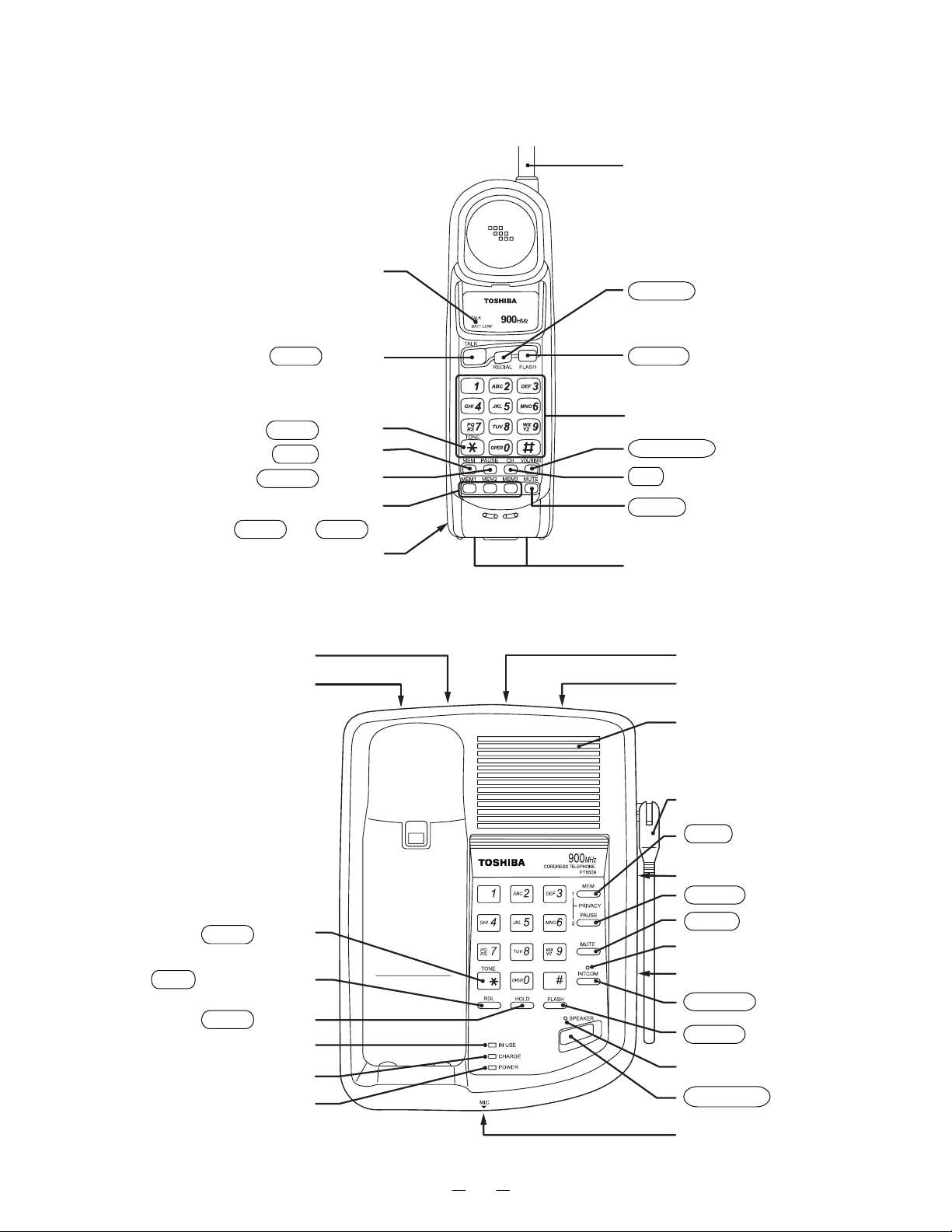
HANDSET CONTROLS AND FUNCTIONS
TALK/BATT.LO W LED
Antenna
REDIAL Button
TALK Button
TONE Button
MEM Button
PAUSE Button
One-touch dialing Button
( MEM1 - MEM3 )
Rechargeable Battery Pac
(back)
BASE UNIT CONTROLS AND FUNCTIONS
DC 9V IN Jack
TEL Line Jac
FLASH Button
Dialpad
VOL/RING Button
CH Button
MUTE Button
Charging Contact
TONE/PULSE Switch
Line Ringer Volume Switch
Speaker
Antenna
TONE Button
RDL (Redial) Button
HOLD Button
IN USE LED
CHARGE LED
POWER LED
MEM (Memory) Button
Speed Dial Index (1 to 10)
PAUSE Button
MUTE Button
INTCOM LED (Green)
Speaker Volume Control
INTCOM Button
FLASH Button
Speaker LED (Green)
SPEAKER Button
Microphone
2
ALIGNMENT PROCEDURE
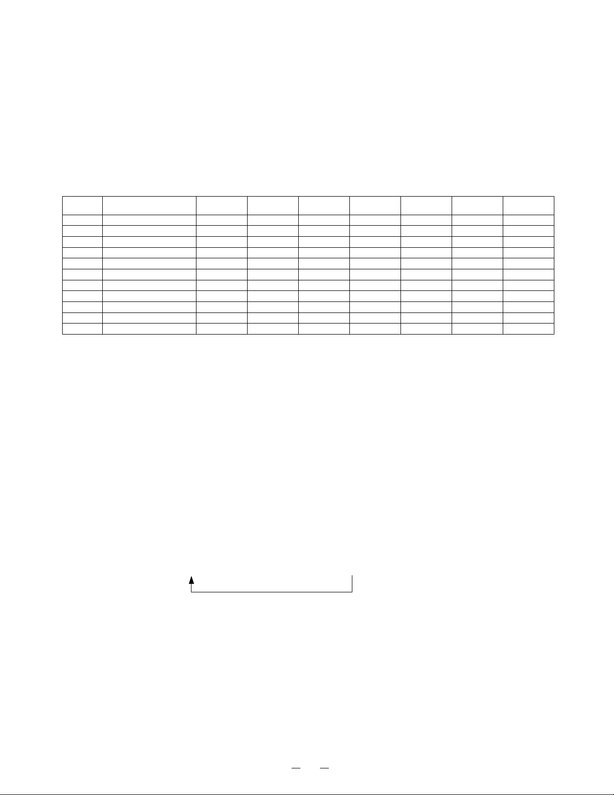
Test Mode For Base Unit
Press the “*” and “#” keys at the same tim e about 1.5 seconds while turning the powe r on, the confirmation
beep will sound to indicate that the unit is in the test mode.
1. To change the TEST mode: Press the number key for the corresponding TEST mode.
(Refer to the following table)
2. To change channel: Press the “RDL” key, but if ch anging the step, the channel returns to the start
channel.
3. To cancel Test mode: Bell rings, charge the Handset or Power off.
STEP FUNCTION KE START CH TX CONT TX MUTE RX MUTE RL CONT REMARKS
1 VO/TX FRQ. ADJ 1 19 L L L L
2 TX MODE CHECK 2 19 L H L H
3TX DATA 3 19 L L L L *1
4 RX SENS. 4 19 H L H H
5 SQ SENS. 5 19 L L H/L H *2
6 RING CHECK 6 19 H L L L
7 DUAL TONE CHECK 7 19 H L L H *3
8 DATA IN CHECK 8 19 L L L H *4
CHANNEL DATA CHECK
9
10 DUPLE 0 19 L H H H
1 1 INT COM MEM 19 L H H L
919H L L L*5
*1 : “0000...” (250Hz) will be fed out continuously as transmitting data.
*2 : Bell rings when sensing SQ.
*3 : Every pushing of FLASH key makes tone change. (In the case of Dual Tone, changes as
1Ö2Ö3Ö4Ö5Ö6Ö7Ö8Ö9Ö0Ö∗Ö#Ö1.)
DTMF Frequency
ROW1 : 697 ROW2 : 770
ROW3 : 852 ROW4 : 941
COL1 : 1209 COL2 : 1336
COL3 : 1477
*4 : Bell rings when the received data are “0000...” (250Hz).
*5 : Charge LED lights when detecting Charge ON.
Channel rotation
19 Ö20Ö21Ö40Ö1Ö2Ö3Ö4Ö5............37Ö38Ö39Ö40
3
Test Mode For Handset Unit
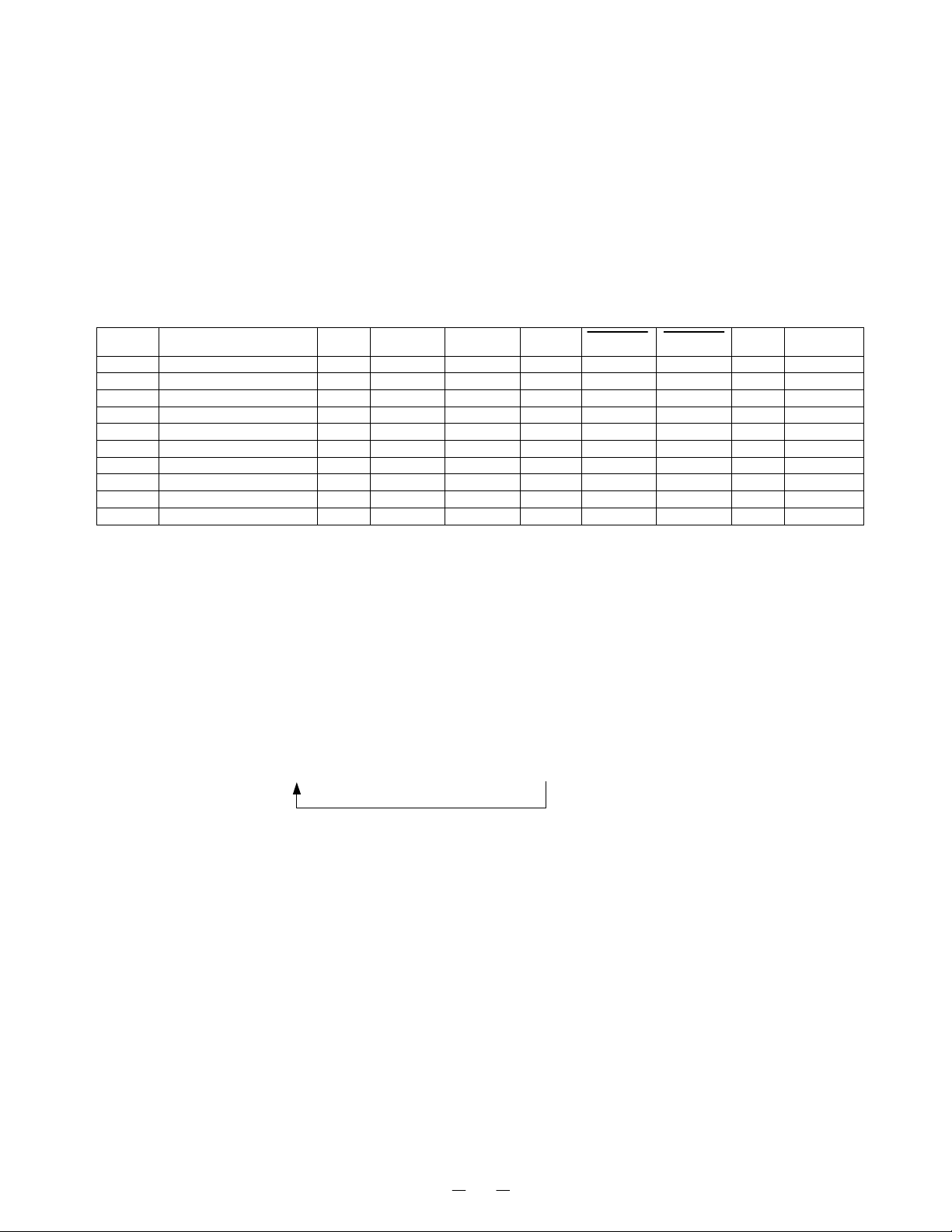
To perform the TEST mode, turn the power ON by pressing the “*” and “#” buttons at the same time.
When entered the TEST mode, the bell rings and the unit enters TEST mode 1. (Refer to the following table.)
1. To change the TEST mode: Press the number key for the corresponding TEST mode.
(Refer to the following table)
2. To change channel: Press “CH” key.
(Note: If the step is changed, the channel returns to the start channel.)
3. To cancel the Test mode: Turn the power OFF, charge the Handset, or press the “TALK” key.
STEP FUNCTION KE START CH TX CONT SC TX MUTE RX MUTE CONV REMARKS
1 VO/TX FRQ. ADJ 1 21 L H L L H
2 TX MOD. CHECK 2 21 L H H L L
3 TX DATA 3 21 L H L L L *1
4 RX SENS. 4 21 H H L H L
5 SQ SENS. 5 21 L H L *A L
6 RECEIVE DATA CHECK 6 21 L H L L H *2
7 BELL 7 21 H L L L H *3
8 BATTERY LOW CHECK 8 21 H L L L H *4
9 CHARGE CHECK 9 21 H L L L H *5
10 DUPLE 0 21 L H H H L
*A : Squelch ON is H, or Squelch OFF is L.
*1 : In the TEST mode 3, “0000...” will be fed out continuously as transmitting data.
*2 : In the TEST mode 6, bell (1kHz) rings when the data received is “0000...”.
*3 : In the TEST mode 7, bell rings with initial 2 tone (2kHz, 2.2kHz).
*4 : In the TEST mode 8, bell (1kHz) rings when P_BATLOW is “L”.
*5 : In the TEST mode 9, bell rings when P_CHRGIN is “L”.
Channel rotation
21 Ö20Ö19Ö40Ö1Ö2Ö3Ö4Ö5............37Ö38Ö39Ö40
4
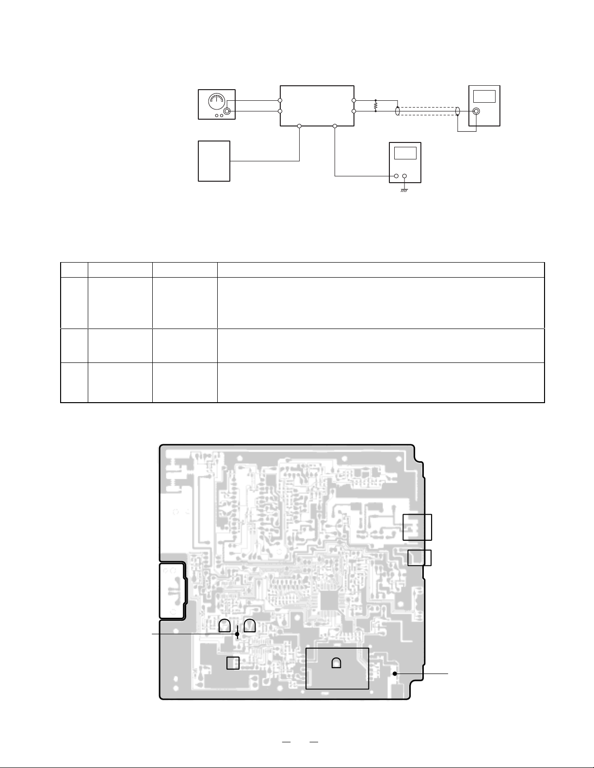
Base Unit
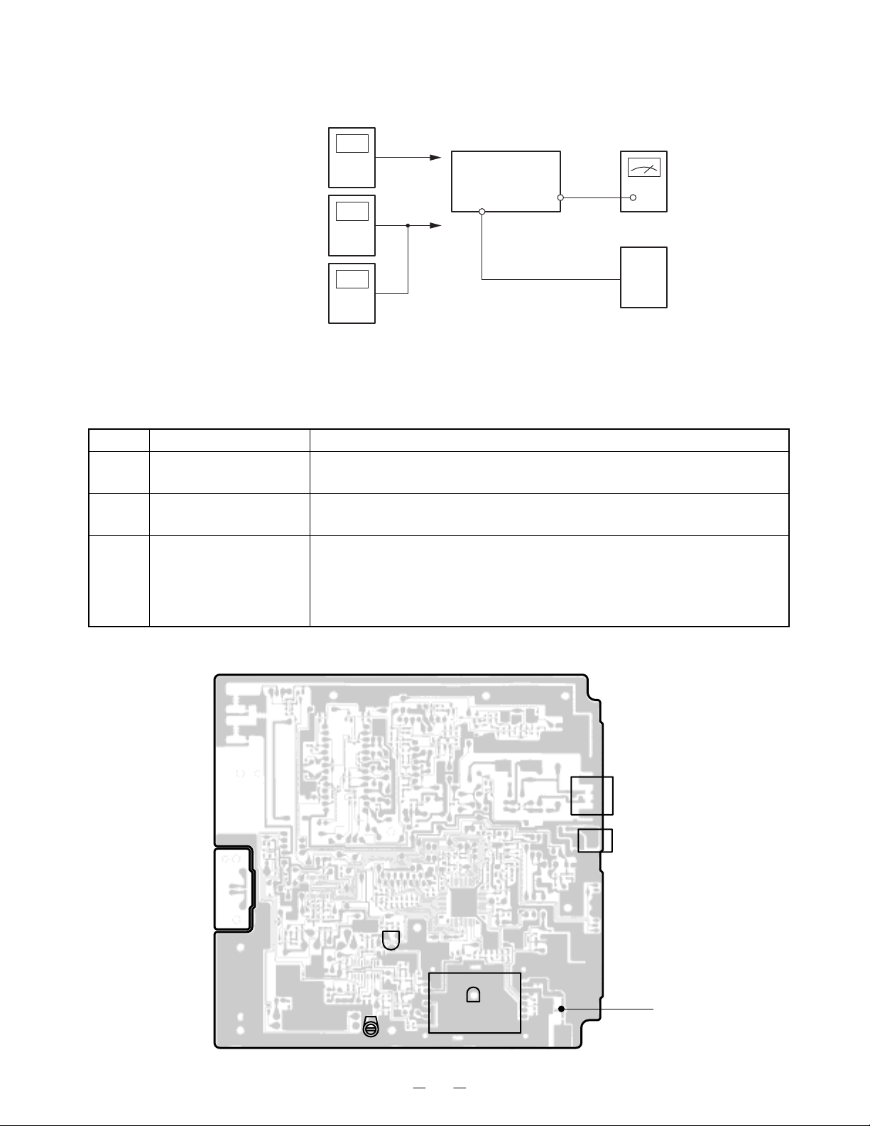
Transmitter Section
Connections
Preset
Place the Base unit in VCO/TX FREQ. ADJ mo de in ac co rdance with the procedure on page 3.
Alignment Procedure
step Adjustment Remarks
1
RT301
(TX Power)
Power
Meter
Frequency
Counter
Deviation
Meter
Connect the Power Meter to the RF test point on the Base MAIN PCB.
Adjust RT301 for a -5.0dBm reading on the Power Meter.
RF
Test Point
RF
Test Point
BASE Unit
J1
DC IN
9V Jack
TEL Line
Jack
J3
1kHz 77.6mV
AF GEN.
AC
Adapter
AC 120V
60Hz
2
CT1
(TX Frequency)
Connect the Freq uency Counter to th e RF test point on the Base MAIN
PCB. Adjust CT1 to make sure that the frequency is 926.897468 MHz.
Press the “2” key to enter the TEST Mode 2. Connect the AF Generator
3
RT3
(TX Modulation)
to the TEL Line Jack on the B ase M ain PCB. Make sure that the o utput
is 1 kHz 77.6 mV from the AF Generator.
Connect the Deviation Meter to the RF test point on the Base MAIN PCB.
Adjust RT3 to indicate ±8 kHz Dev.
Alignment Point Location on Base Main PCB and Base RF PCB
Base Main PCB
J3
TEL LINE Jack
J1
DC IN 9V Jack
CT1
RT3
BASE RF PCB
RT301
5
RF TEST POINT
Receiver Section
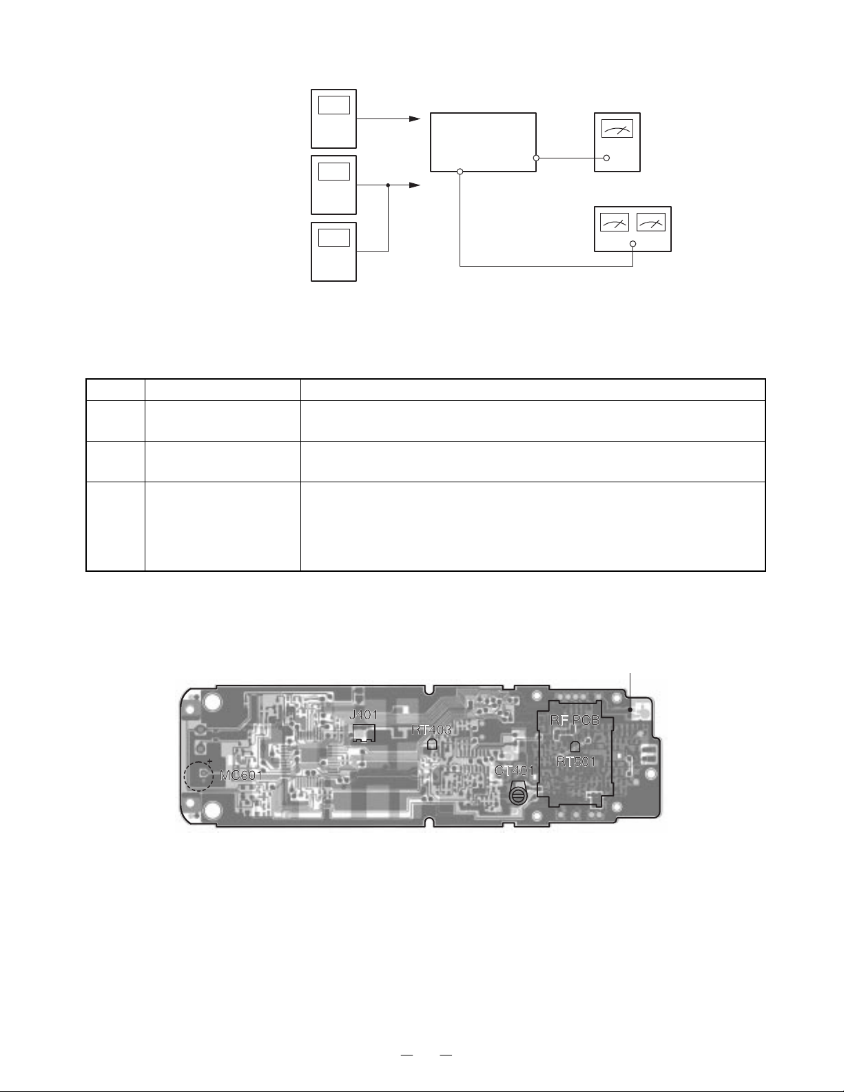
Connections
RF SG
+
BASE Unit
RF
Test Point
TEL Line
Jack
J3
Dummy Load
(600-ohm)
-
+
AC Voltmeter
AF
Terminal
DC Voltmeter
AC 120V
60Hz
DC IN 9V Jack
J1
AC
Adapter
Preset
Place the Base unit in RX SENS mode (step 4) in accordance with the procedure on page 3.
Alignment Procedure
step Preset to Adjustment Remarks
Connect the RF Signal Generator to the RF t est point on the Base MAIN
PCB. Make sure that the frequency is 902.952467 MHz.
Connect the DC Voltmeter to the AF test p oint (JV21). Adjust L3 to
indicate DC 1.9V.
Connect the AC Voltmeter across a 600-ohm dummy to the Telephone
Line Jack. Adjust RT2 for a 218 mV reading on the AC voltmeter.
Press the “5” key to enter the TEST Mode 5. Make sure that the
frequency of RF SG output is 902.952467 MHz. Adjust RT1 to turn to
the point where the bell rings.
1
SG: 1mV
No modulation
SG: 1mV
2
1kHz ±8kHz
deviation
SG: -7dBµV
3
No modulation
L3
(Discriminator
Voltage)
RT2
(RX AF
Voltage)
RT1
(SQ Point)
Alignment Point Location on Base Main PCB and Base RF PCB
Base Main PCB
RT1
RT2
AF TEST POINT
JV21
L3
BASE RF PCB
RT301
J3
TEL LINE Jack
J1
DC IN 9V Jack
RF TEST POINT
6
Handset Unit
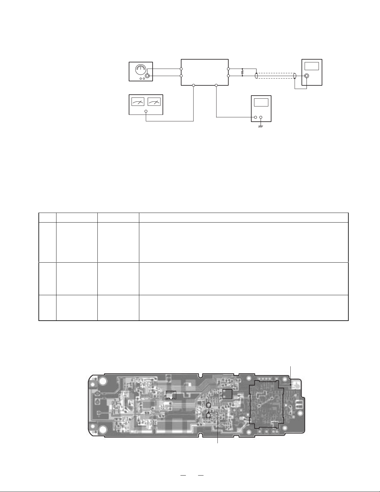
Transmitter Section
Connection
Preset
Place the Handset in VCO/TX FREQ. ADJ mode in accordance with the procedure on page 4.
Alignment Procedure
step Adjustment Remarks
1
RT501
(TX Power)
Power
Meter
Frequency
Counter
Deviation
Meter
Connect the RF Power Met er to the RF test point on the Handset MAI
PCB. Adjust RT501 for a -7.5dBm reading on the Power Meter.
RF
Test Point
RF
Test Point
HANDSET Unit
J401
Batter
Terminals
MIC+Pin
DC 3.8V
AF GEN.
1kHz 9mV
DC Power Supply
2
CT401
(TX Frequency)
Connect the Fre quenc y Counter to th e RF t est p oint on the handset M AIN
PCB. Adjust CT401 to make sure that the frequency is 903.052467 MHz.
Press the “2” key to enter the TEST Mode 2. Connect the AF Generator
3
RT403
(TX Modulation)
to the MIC Connector make sure that the output is 1kHz 9mV from the AF
Generator.
Connect the De viation Meter to the RF test poi nt on the handset MAIN
PCB. Adjust RT403 to indicate ±8 kHz Dev.
Alignment Point Location on Handset Main PCB and Handset RF PCB
Handset PCB
RF TEST POINT
7
Receiver Section
Connections
RF SG
+
RF
Test Point
HANDSET Unit
Connector
SP
Dummy Load
(150-ohm)
-
+
AC Voltmeter
DC Power Supply
J401
Batter
Terminal
DC 3.8V
AF
Terminal
DC Voltmeter
Preset
a) Connect the handset RF unit to the handset main unit.
b) Connect DC power supply to battery connector on the handset unit.
c) Turn the DC power supply O N while pressing “ *” and “#” k eys, and keep pressin g the key cont inuously for
approximate 2 seconds.
d) Release keys when entering TEST mode 1 with TALK LED lighting and beep.
Alignment Procedure
step Preset to Adjustment Remarks
Press the “4” key to enter the TEST Mode 4. Connect the RF Signal
1
SG: 1mV
No modulation
SG: 1mV
2
1kHz ±8kHz
Deviation
L402
(Discriminator
Voltage)
RT402
(RX AF
Voltage)
Generator to the RF test point on the handset MAIN PCB. Make sure
that the frequency is 926. 997 467 MHz.
Connect the DC Vo ltmeter to the AF test point. Adjust L402 t o indicate
DC 1.00 V.
Connect the RF Signal Generator to the RF test point on the handset
MAIN PCB. Make sure that the frequency is 926.997467 MHz.
Connect the AC Voltmeter across a 150-ohm dummy to the MIC
Connector. Adjust RT402 for a 128 mV reading on the AC Voltmeter.
Press the “5” key to enter the TEST Mode 5. Make sure that the frequency
of RF SG output is 926.997467 MHz. Adjust RT401 to turn to the point
where the bell rings.
3
SG: -7dBµV
1kHz ±8kHz
Deviation
RT401
(SQ Point)
Alignment Point Location on Handset Main PCB and Handset RF PCB
Handset PCB
J401
RT402
RT401
AF TEST POINT
8
L402
RF PCB
RF TEST POINT
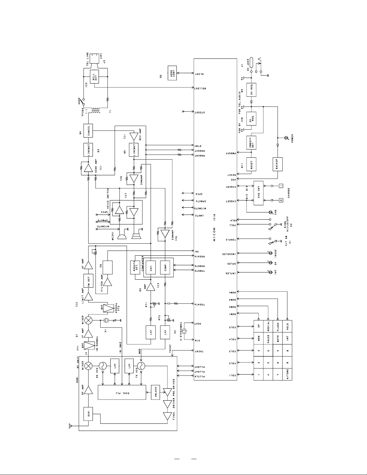
Base Unit
BLOCK DIAGRAMS
9
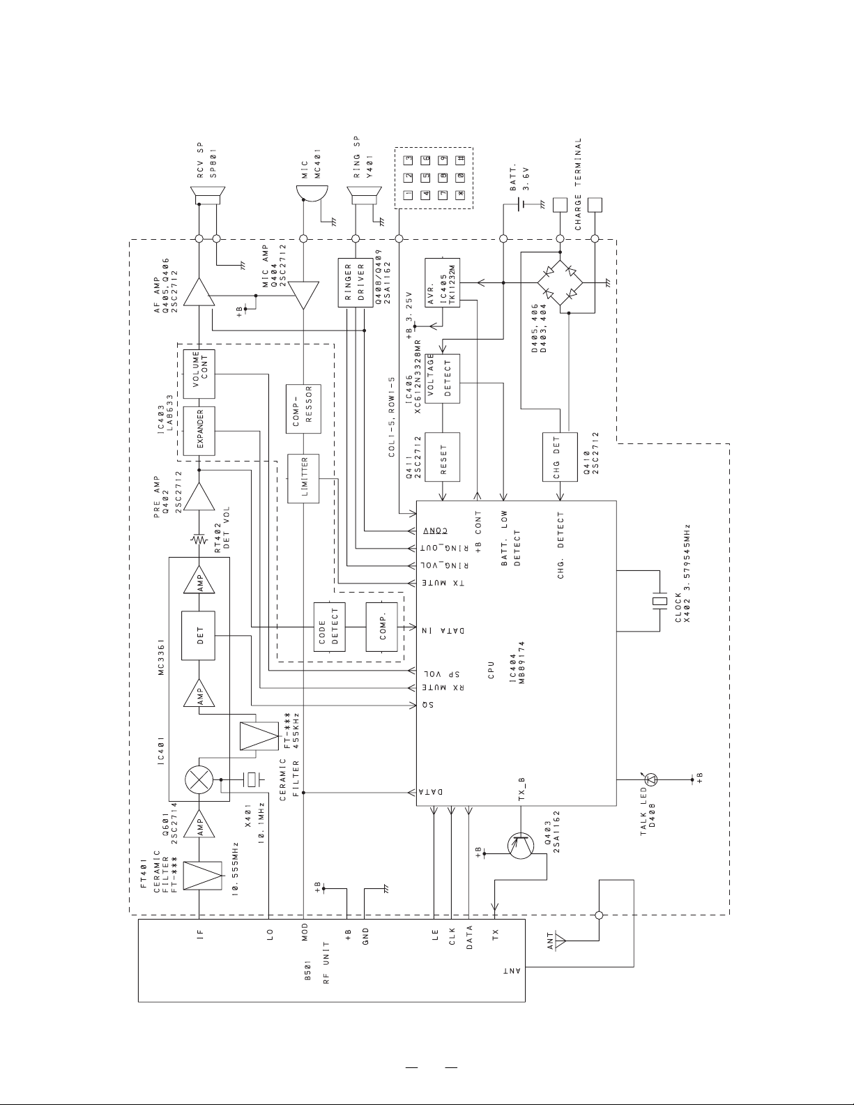
Handset Unit
10
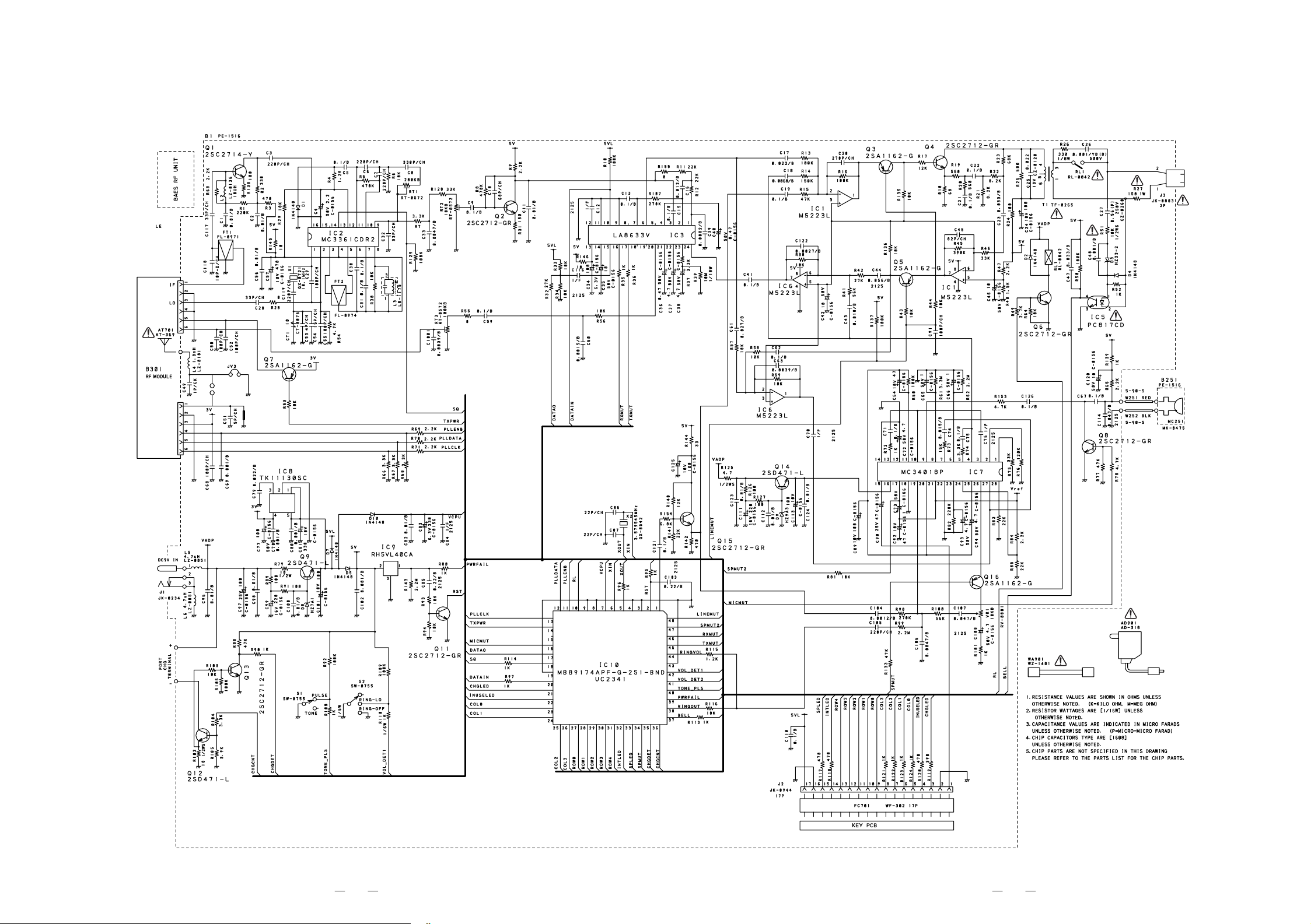
%DVH#8QLW/#0DLQ
6&+(0$7,&#',$*5$06
4544
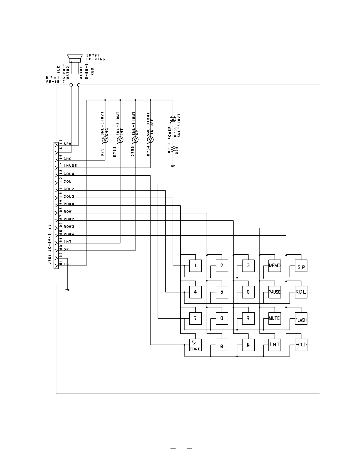
Base Unit, ke
NOTES:
1. RESISTANCE VALUES ARE SHOWN IN OHMS UNLESS
OTHERWISE NOTED. (K=KILO OHM, M=MEG OHM)
13
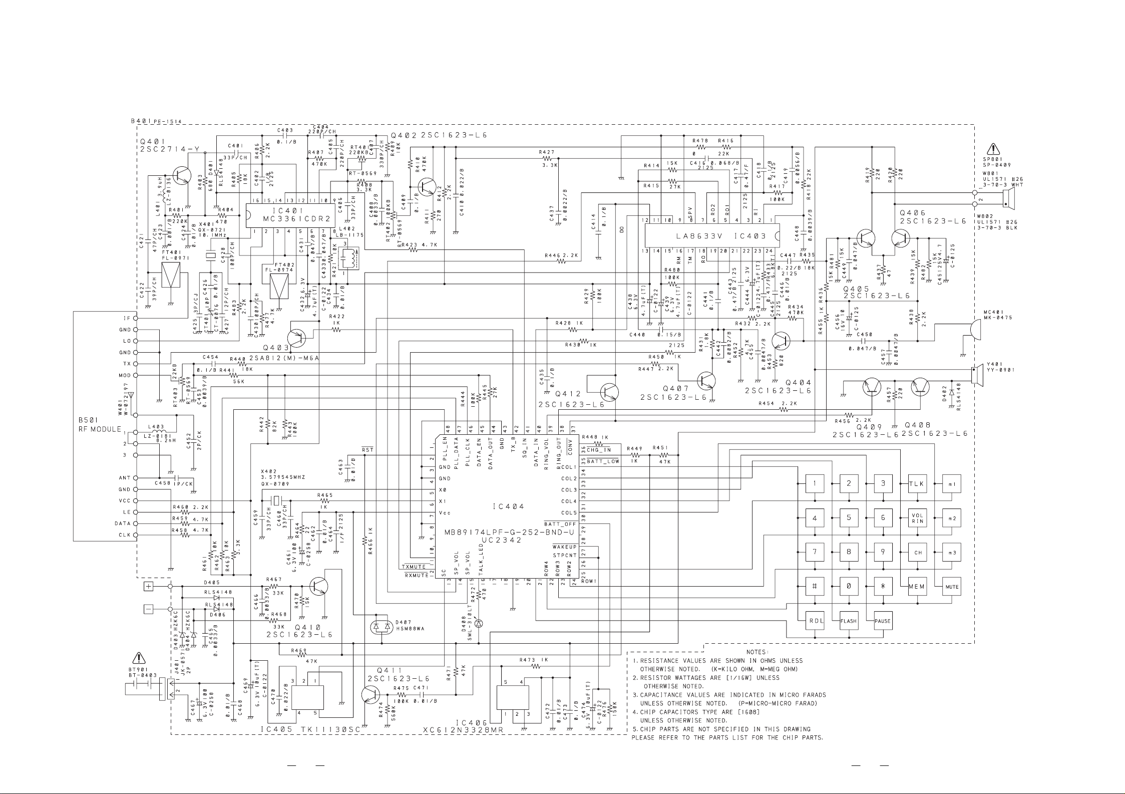
+DQGVHW/#0DLQ
##
4847
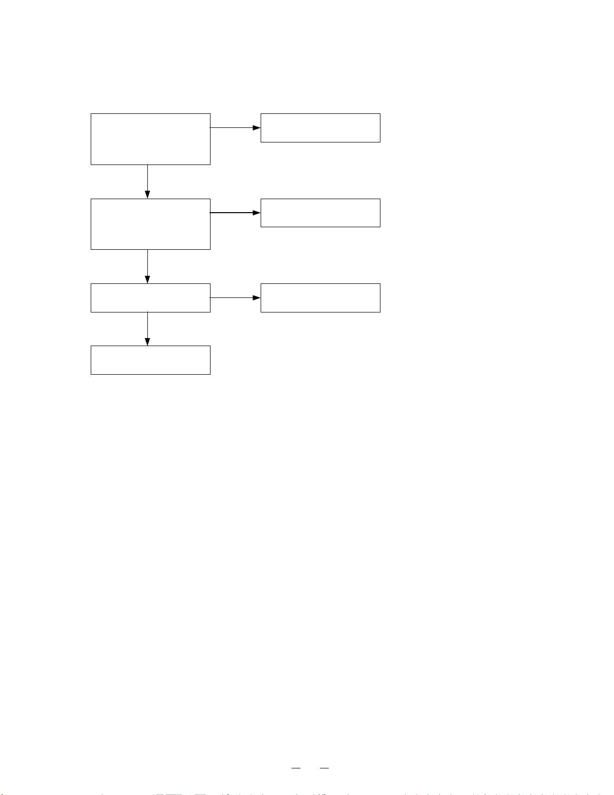
TROUBLESHOOTING HINTS
1. The bell does not ring.
When the INTCOM key of
the base is pressed, does
the ringer on the handset
ring?
OK
When the TEL SG is joined
with the base to make bell
signal, is there pulse wave
at pin 4 of IC5?
OK
Is there pulse wave at pin
37 of IC10?
OK
Check IC10 and its
periphe ral circuit.
NG
NG
NG
See 2. The bell does not
ring & page does not ring.
Check IC5 and TEL network
circuit.
Check R50, R113 and C47.
16
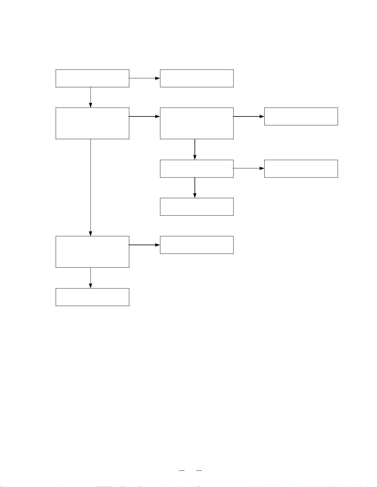
2. The bell does not ring & page does not ring.
Can the base and handset
be connected?
OK
Press handset DIAL key
while in TALK MODE.
Can key touch sound be
heard from the ringer?
OK
When the INTCOM key of
the base is pressed, does
pin 14 of IC10 change from
to low?
OK
NG
NG
NG
See 3. The base and handset
cannot be connected.
When the ke y of the handset
is pressed, can the pulse
output at pin 38 of IC404 be
seen?
OK
At the Q408 collector, can
the pulse wave be seen?
OK
Check RINGER Y401.
Check Keyboard Rub ber.
NG
NG
Check IC404.
Check R454, R457, R456,
Q408, Q409 and D402.
Check IC10 and its
periphe ral circuit.
17
 Loading...