

Page 1

FILE NO. 2B0-9801
SERVICE MANUAL
CORDLESS TELEPHONE
FT-8258
PUBLISHED IN JAPAN, Jun., 1998
Page 2

CONTENTS
SAFETY PRECAUTIONS ......................................................................................................................1
OPERATING CONTROLS.....................................................................................................................2
ALIGNMENT PROCEDURE..................................................................................................................3
BLOCK DIAGRAMS...............................................................................................................................9
SCHEMATIC DIAGRAMS....................................................................................................................14
TROUBLESHOOTING HINTS.............................................................................................................24
IC AND TRANSISTOR VOLTAGE CHART ......................................................................................... 31
SEMICONDUCTOR LEAD IDENTIFICATION.....................................................................................38
ELECTRICAL PARTS LOCATION ......................................................................................................42
WIRING DIAGRAMS ...........................................................................................................................47
EXPLODED VIEW AND MECHANICAL PARTS LIST ........................................................................49
PARTS LIST ........................................................................................................................................53
ASSEMBLY PARTS LIST ....................................................................................................................75
SPECIFICATIONS ...............................................................................................................................76
SAFETY PRECAUTIONS
Before returning any models to the customer, a safety check of the entire instrument should be made.
The service technician must be sure that no protective device built into the instrument by the manufacturer
has become defective or inadvertently degraded during servicing.
1. WARNING:
Alterations of the design or circuitry of these models should not be made.
Any design changes or additions such as, but not limited to, circuit modifications, auxiliary speaker
jacks, switches, grounding, active or passive circuitry, etc. may alter the safety characteristics of these
models and potentially create a hazardous situation for the user.
Any design alterations or additions will void the manufacturer’s warranty and will further relieve the
manufacturer of responsibility for personal injury or property damage resulting therefrom.
2. PRODUCT SAFETY NOTICE
Many electrical and mechanical parts in this chassis have special characteristics. These characteristics
often pass unnoticed and the protection afforded by them cannot necessarily be obtained by using
replacement components rated for higher voltage, wattage, etc. Replacement parts that have these
special safety characteristics are identified in this manual and its supplements; electrical components
having such features are identified by a
any of these components, read the parts list in this manual carefully. The use of substitute replacement
parts that do not have the same safety characteristics as specified in the parts list may create shock, fire
or other hazards.
in the schematic diagram and the parts list. Before replacing
— 1 —
Page 3
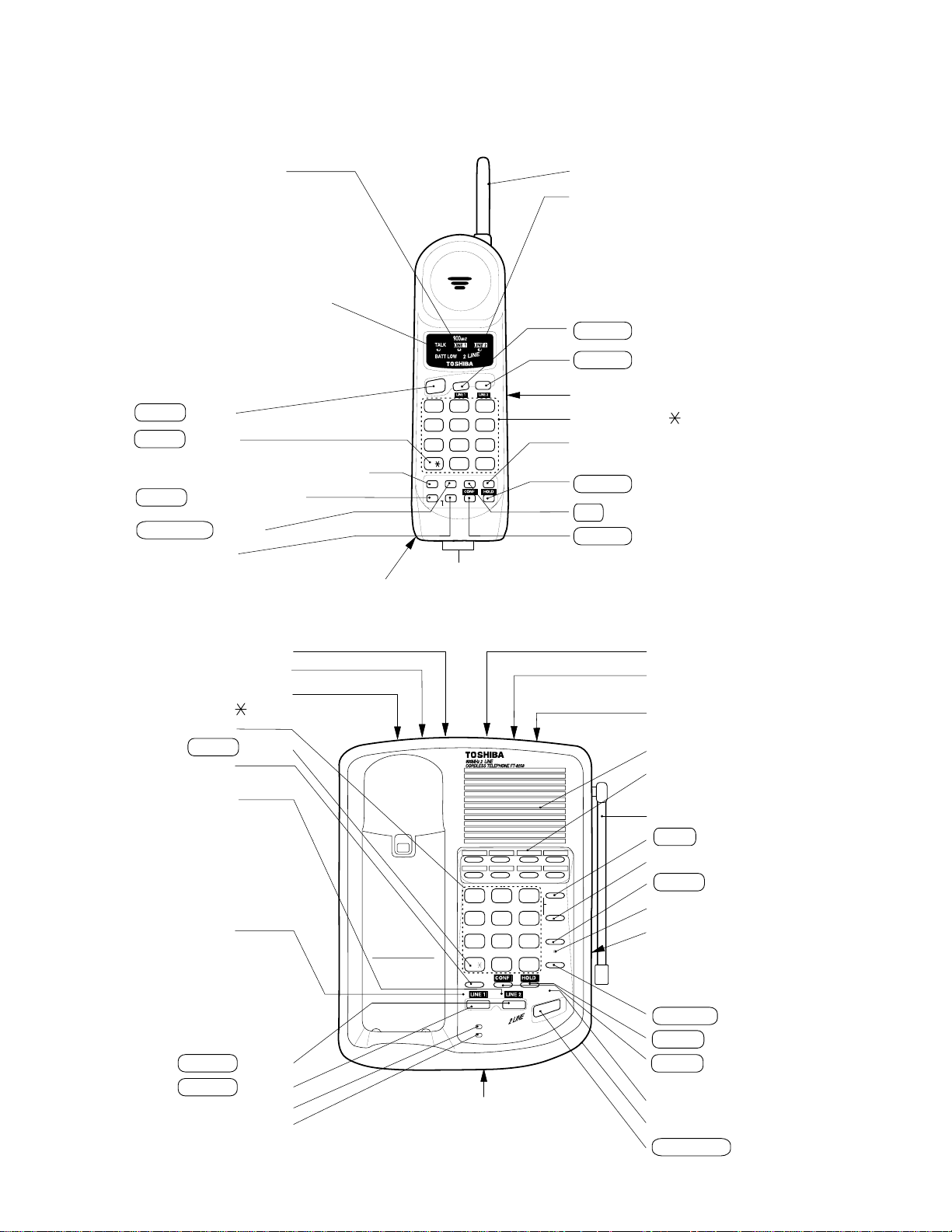
HANDSET CONTROLS
OPERATING CONTROLS
LINE 1 LED (Green)
• Lights when the handset is used for
a phone conversation on line 1.
• Blinks when the base unit or
additional phone is in use on line 1.
• Blinks when line 1 is put on hold.
• Blinks when line 1 is ringing.
TALK/BATT LOW LED (Red)
Standby status : OFF
•
•
Lights ON during a phone
conversation using the handset.
•
Blinks when a channel is changed,
and during the low battery status
and mute status.
TALK button
TONE button
FLASH/RDL (Flash/Redial) button
MEM (Memory) button
INTCOM button
PAUSE button
TALK
ABC DEF
123
JKL MNOGHI
456
PQ
RS
TONE
FLASH/RDL INTCOM CH
MEM
WX
TUV
YZ
789
OPER
0#
VOL/RING
PAUSE
12
PRIVACY
Charging Contacts
Battery compartment (back)
Antenna
LINE 2 LED (Orange)
•
Lights when the handset is used for
a phone conversation on line 2.
•
Blinks when the base unit or
additional phone is in use on line 2.
•
Blinks when line 2 is put on hold.
•
Blinks when line 2 is ringing.
LINE 1 button
LINE 2 button
SPEED DIAL INDEX (back)
Dialpad (1~9, and # Dial Buttons)
VOL/RING
(Volume/Ringer volume) button
HOLD button
CH (Channel) button
CONF (Conference) button
BASE UNIT CONTROLS
DC IN 9V jack
TEL LINE 2 jack
TEL LINE 1/2 jack
Dialpad (1~9, and #
Dial Buttons)
TONE button
FLASH/RDL
(Flash/Redial) button
LINE 2 LED (Orange)
Lights when the base unit is used
•
for a phone conversation on line 2.
• Blinks when the handset or
additional phone is in use on
line 2.
• Blinks when line 2 is put on hold.
• Blinks when line 2 is ringing.
LINE 1 LED (Green)
•
Lights when the base unit is used
as speaker phone on line 1.
• Blinks when the handset or
additional phone is in use on
line 1.
• Blinks when line 1 is put on hold.
• Blinks when line 1 is ringing.
LINE 2 button
LINE 1 button
CHARGE LED
POWER LED
ABC DEF
12 3
JKL MNOGHI
45 6
PQ
TUV
789
RS YZ
TONE
OPER
0
FLASH/RDL
MHZ
900
CHARGE
POWER
Microphone
Tone/Pulse switch
Line 1 ringer
volume switch
Line 2 ringer
volume switch
Speaker
One-touch dialing keys
(1 to 8)
Antenna
MEM (Memory) button
PAUSE button
MEM
1
PRIVACY
PAUSE
2
MUTE
WX
INTCOM
#
SPEAKER
MUTE button
INTCOM LED (Green)
SPEED DIAL INDEX
• Pull out the SPEED DIAL INDEX
card to find out a destination name
associated with a number preset
in the speed dial memory.
INTCOM button
HOLD button
CONF (Conference)
button
SPEAKER LED (Green)
SPEAKER volume control
SPEAKER button
— 2 —
Page 4
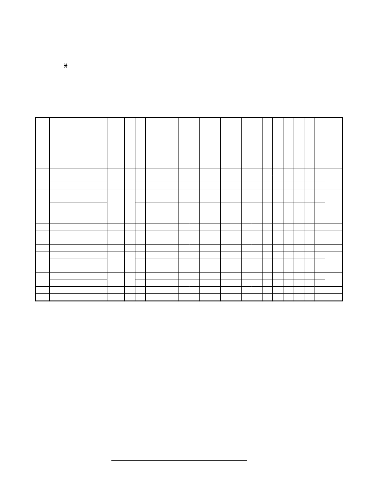
ALIGNMENT PROCEDURE
Test Mode For Base Unit
Press the “ ” and “#” keys at the same time about 1.5 seconds while turning the power on, the confirmation beep will
sound to indicate that the unit is in the test mode.
1. To change the TEST mode: Press the number key for the corresponding TEST mode.
(Refer to the following table)
2. To change channel: Press the “FLASH/RDL” key, but if changing the step, the channel returns to the
start channel.
3. To cancel Test mode: Bell rings, charge the Handset, or press the “SPEAKER” key.
K
S
T
T
R
R
R
C
C
S
S
I
C
D
D
D
D
S
S
M
E
T
X
X
X
L
L
T
T
P
P
N
N
T
T
T
T
P
S
T
E
P
1VCO/TX FRQ. ADJ 1 19LLL LLLLLLLLLLLLHHH
3TX DATA 3 19LLLLLLLLLLLLLLLHHH*2
5SQ SENS 5 19LLH/LHLHLLLLLLLLLHHH*3
6BELL MODULATION 6 19LHLHLHLLLLLLLLLHHH
7RINGER CHECK 7 19HLL LLLLLLLLLLLLHHH*4
8DATA IN CHECK 8 19LLHHLHLLLLLLLLLHHH*5
9CHANNEL DATA 9 19HLLLLLLLLLLLLLLHHH*6
11
12INTERCOM HOLD19LHH/LLLLLLLHLLLLLLLL *8
13ON HOOK PARA INT’C19HHL LLLLLLLLLLLLHHH *9
FUNCTION
TX CHECK L1 LHLHLHLLLLLLLLLHHH
TX CHECK L2 L H L L H L H L L L L L L L L H H H2
TX CHECK L1 + L2
RX SENS L1 HLHHLHLLLLLLLLLHHH
RX SENS L2 H L H L H L H L L L L L L L L H H H4
RX SENS L1 + L2
DUPLEX L1 LHHHLHLLLLLLLLLHHH
DUPLEX L2 LHHLHLHLLLLLLLLHHH10
DUPLEX L1 + L2
DUAL TONE L1 H L L H L L L L L L L H L L H H H H*1
DUAL TONE L2
Y
219
419
019
MEM 19
A
P
M
M
C
C
1
2
1
2
T
F
M
M
M
R
W
U
U
N
N
P
P
P
P
P
P
F
T
R
T
T
T
T
A
A
A
A
A
E
E
1
2
S
S
S
C
H
LHLHHHHLLLHLLLLHHH
HLHHHHHLLLHLLLLHHH
LHHHHHHLLLHLLLLHHH
HLLLHLLLLLLLHLHHHH *7
S
A
S
S
F
L
L
1
2
M
F
F
S
E
P
N
P
K
K
C
A
S
M
P
*1 : Switch the line with LINE1, LINE2, and CONF keys, the corresponding LED lights.
*2 : “0000...” (250Hz) will be fed out continuously as transmitting data.
*3 : INTCOM LED lights when sensing SQ.
*4 : INTCOM LED lights when detecting BELL.
*5 : INTCOM LED lights when the received data are “0000...” (250Hz).
(In the case of Dual Tone, changes as 1→ 2 → 3 → 4 →5 → 6 →7 → 8 → 9 → 0 → * → # → 1.)
*6 : Charge LED lights when detecting Charge ON.
*7 : Every pushing of PAUSE key makes tone change.
DTMF Frequency
ROW1 : 697 ROW2 : 770
ROW3 : 852 ROW4 : 941
COL1 : 1209 COL2 : 1336
COL3 : 1477
*8 : RX Mute turns on or off when pushing MUTE key. (Off initially, on when pushed.)
*9 : LINE LED lights as follows according to the condition of the telephone used together.
ON Hook : ON
OFF Hook : Blinking
No Connection : OFF
Channel rotation
R
I
E
C
M
M
A
U
R
T
K
E
S
*
1
*
1
*
1
19 → 20 → 21 → 40 → 1 → 2 → 3 → 4 → 5 . . . . . . . . 37 → 38 → 39 → 40
↑
— 3 —
Page 5
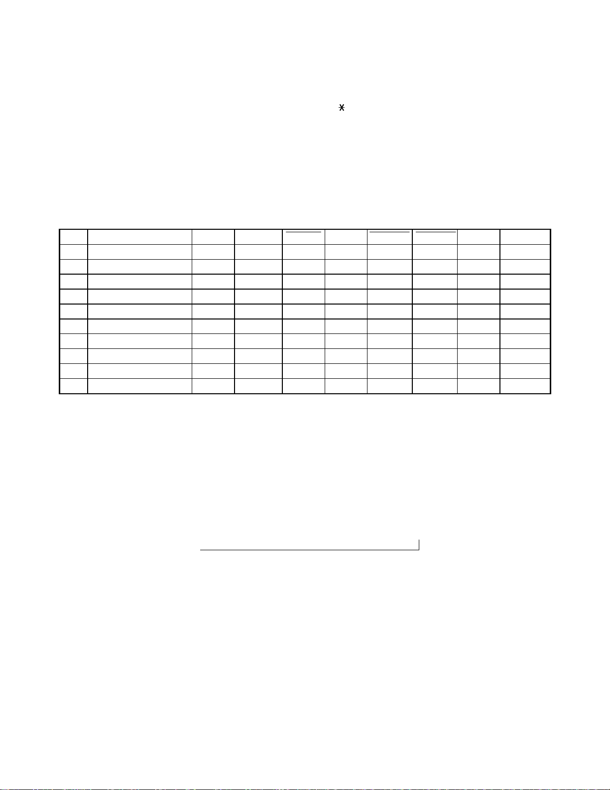
Test Mode For Handset Unit
To perform the TEST mode, turn the power ON by pressing the “ ” and “#” buttons at the same time.
When entered the TEST mode, the bell rings and the unit enters TEST mode 1 . ( Refer to the following table. )
1. To change the TEST mode: Press the number key for the corresponding TEST mode.
(Refer to the following table)
2. To change channel: Press “CH” key.
( Note: If the step is changed, the channel returns to the start channel. )
3. To cancel the TEST mode: Turn the power OFF, charge the Handset, or press the “TALK” key.
STEP FUNCTION KEY START CH TX PWR RX PWR TX MUTE RX MUTE CONV REMARKS
1 VCO/TX FREQ. ADJ 1 21 L H H L H
2 TX MOD. CHECK 2 21 L H L L L
3TX DATA 3 21 L H L L L
4RX SENS 421HHLHL
5SQ SENS 5 21 L H L *A L
6 RECEIVE DATA CHECK 6 21 L H L L H
7 BELL 7 21 H L L L H
8 BATTERY LOW CHECK 8 21 H L L L H
9 CHARGE CHECK 9 21 H L L L H
10 DUPLEX 0 21 L H H H L
*
1
*
2
*
3
*
4
*
5
*A : Squelch ON is H, or Squelch OFF is L.
*1 : In the TEST mode 3, “0000...” will be fed out continuously as transmitting data.
*2 : In the TEST mode 6, bell (1kHz) rings when the data received is “0000...”.
*3 : In the TEST mode 7, bell rings with initial 2 tone (2kHz, 2.2kHz).
*4 : In the TEST mode 8, bell (1kHz) rings when P_BATLOW is “L”.
*5 : In the TEST mode 9, bell rings when P_CHRGIN is “L”.
Channel rotation
21 → 20 → 19 → 40 → 1 → 2 → 3 → 4 → 5 . . . . . . . . 37 → 38 → 39 → 40
↑
— 4 —
Page 6
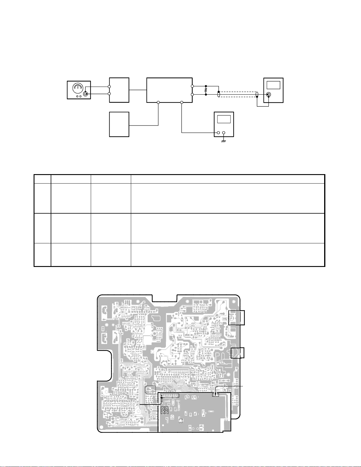
Base Unit
V
Transmitter Section
Connection
Power
Meter
Frequency
Counter
Deviation
Meter
RF
Test Point
RF
Test Point
BASE RF PCB
RF
Test Point
BASE MAIN PCB
J2
DC IN
9V Jack
TEL Line
1/2 Jack
AF GEN.
J5
1kHz 61.0mV
AC
Adapter
Preset
Place the Base Unit in VCO/TX FREQ ADJ mode in accordance with the procedure on page 3.
Alignment Procedure
Step Adjustment Remarks
1
2
3
VR202
(TX Power)
CT201
(TX Frequency)
RT2
(TX Modulation)
Connect the Power Meter to the RF test point on the Base RF PCB. Adjust
VR202 for a
−
4 dBm reading o n the Power Meter.
Connect the Frequency Counter to the RF test point on the Base RF PCB.
Adjust CT201 to make sure that the frequency is 926.900494 MHz.
Press the “2” key to enter the TEST Mode 2. Connect the AF Generator to
the TEL Line Jack on the Base Main PCB. Make sure that the output is 1
kHz 61.0 mV from the AF Generator.
Connect the Deviation Meter to the RF test point on the Base RF PCB.
Adjust RT2 to indicate
±
8 kHz Dev.
AC 120
60Hz
Alignment Point Location on Base Main PCB and Base RF PCB
Base Main PCB
RT2
Base RF PCB
J201
CT201
VR202
— 5 —
J5
TEL LINE 1/2 Jack
J2
DC IN 9V Jack
RF TEST POINT
Page 7
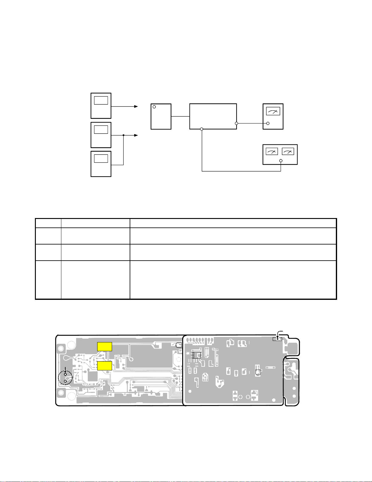
Receiver Section
Connection
RF SG
AC 120V
60Hz
BASE RF PCB
−
RF
+
Test Point
AC
Adapter
BASE MAIN PCB
J2
DC IN
9V Jack
TEL Line
1/2 Jack
J5
−
+
J1
AF Term i n a l
Dummy Load
(600-ohm)
DC Voltmeter
AC Voltmeter
Preset
Place the Base Unit in RX SENS mode (step 4) in accordance with the procedure on page 3.
Alignment Procedure
Step Preset to Adjustment Remarks
Connect the RF Signal Generator to the RF test point on the Base RF
PCB. Make sure that the frequency is 902.979122 MHz.
Connect the DC Voltmeter to the J1 AF test point. Adjust L212 to indicate
DC 0.95 V.
Connect the RF Signal Generator to the RF test point on the Base RF
PCB. Make sure that the frequency is 902.979122 MHz.
Connect the AC Voltmeter across a 600-ohm dummy to the Telephone
Line Jack. Adjust R T1 for a 218 mV reading on the AC voltmeter.
Press the “5” key to enter the TEST Mode 5. Make sure that the
frequency of RF SG output is 902.979122 MHz. Adjust VR201 to turn to
the point where the INTCOM LED just turns on.
1
SG: 1mV
No modulation
SG: 1 mV
2
1 kHz ±8kHz
deviation
SG:
3
No modulation
−7
dBµV
L212
(Discriminator
Voltage)
RT1
(RX AF
Voltage)
VR201
(SQ Point)
Alignment Point Location on Base Main PCB and Base RF PCB
Base Main PCB
Base RF PCB
RT1
AF TEST POINT
J1
L212
VR201
— 6 —
J201
J5
TEL LINE 1/2 Jack
J2
DC IN 9V Jack
RF TEST POINT
Page 8
Handset Unit
Transmitter Section
Connection
Power
Meter
Frequency
Counter
Deviation
Meter
RF
Test Point
RF
Test Point
HANDSET RF PCB
RF
Test Point
HANDSET MAIN PCB
Battery
Terminals
MIC + Pin
AF GEN.
1kHz 11.0mV
DC Power Supply
DC 3.8V
Preset
Place the Handset in VCO/TX FREQ. ADJ mode in accordance with the procedure on page 4.
Alignment Procedure
Step Adjustment Remarks
1
2
3
VR502
(TX Power)
CT501
(TX Frequency)
VR601
(TX Modulation)
Connect the RF power Meter to the RF test point on the handset RF PCB.
Adjust VR502 for a −6 dBm reading on the Power Meter.
Connect the Frequency Counter to the RF test point on the handset RF
PCB. Adjust CT 501 to make sure that the frequency is 903.079230 M Hz.
Press the “2” key to enter the TEST Mode 2. Connect the AF Generator to
the MIC Connector. Make sure th at the ou tput is 1 kHz 11.0 mV from the AF
Generator.
Connect the Deviation Meter to the RF test point on the handset RF PCB.
Adjust VR601 to indicate ± 8kHz Dev.
Alignment Point Location on Handset Main PCB and Handset RF PCB
Handset Main PCB RF PCB
MIC + Pin
MC601
−
Battery Terminals
+
VR601
CT501
— 7 —
RF TEST POINT
J501
VR502
Page 9
Receiver Section
Connection
RF SG
HANDSET RF PCB
−
RF
+
Test Point
DC Power Supply
HANDSET MAIN PCB
DC 3.8V
Battery
Terminals
J602
SP
Connector
J601
AF Terminal
−
+
Dummy Load
(150-ohm)
DC Voltmeter
AC Voltmeter
Preset
Place the Handset in RX SENS mode (step 4) in accordance with the procedure on page 4.
Alignment Procedure
Step Preset to Adjustment Remarks
Connect the RF Signal Generator to the RF test point on the handset RF
PCB. Make sure that the frequency is 927.000602 MHz.
Connect the DC Voltmeter to the J601 AF test point. Adjust L512 to
indicate DC 0.95 V.
Connect the RF Signal Generator to the RF test point on the handset RF
PCB. Make sure that the frequency is 927.000602 MHz.
Connect the AC Voltmeter across a 150-ohm dummy to the SP
Connector. Adjust VR602 for a 60 mV reading on the AC Voltmeter.
Press the “5” key to enter the TEST Mode 5. Make sure that the
frequency of RF SG output is 927.000602 MHz. Adjust VR501 to turn to
the point where the LINE 1 LED just turns on.
SG: 1 mV
1
No modulation
SG: 1 mV
2
1 kHz ±8 kHz
deviation
SG:
3
1 kHz ±8 kHz
deviation
−7 dBµV
L512
(Discriminator
Voltage)
VR602
(RX AF
Output)
VR501
(SQ Point)
Alignment Point Location on Handset Main PCB and Handset RF PCB
Handset Main PCB
−
Battery Terminals
+
AF TEST POINT
RF PCB
J601
VR602
L512
VR501
— 8 —
RF TEST POINT
J501
J602
SP
Connector
Page 10
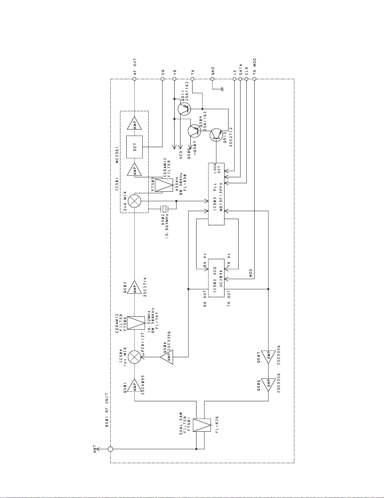
Handset, Main
BLOCK DIAGRAMS
—9 —
Page 11
Handset, RF
— 10 —
Page 12
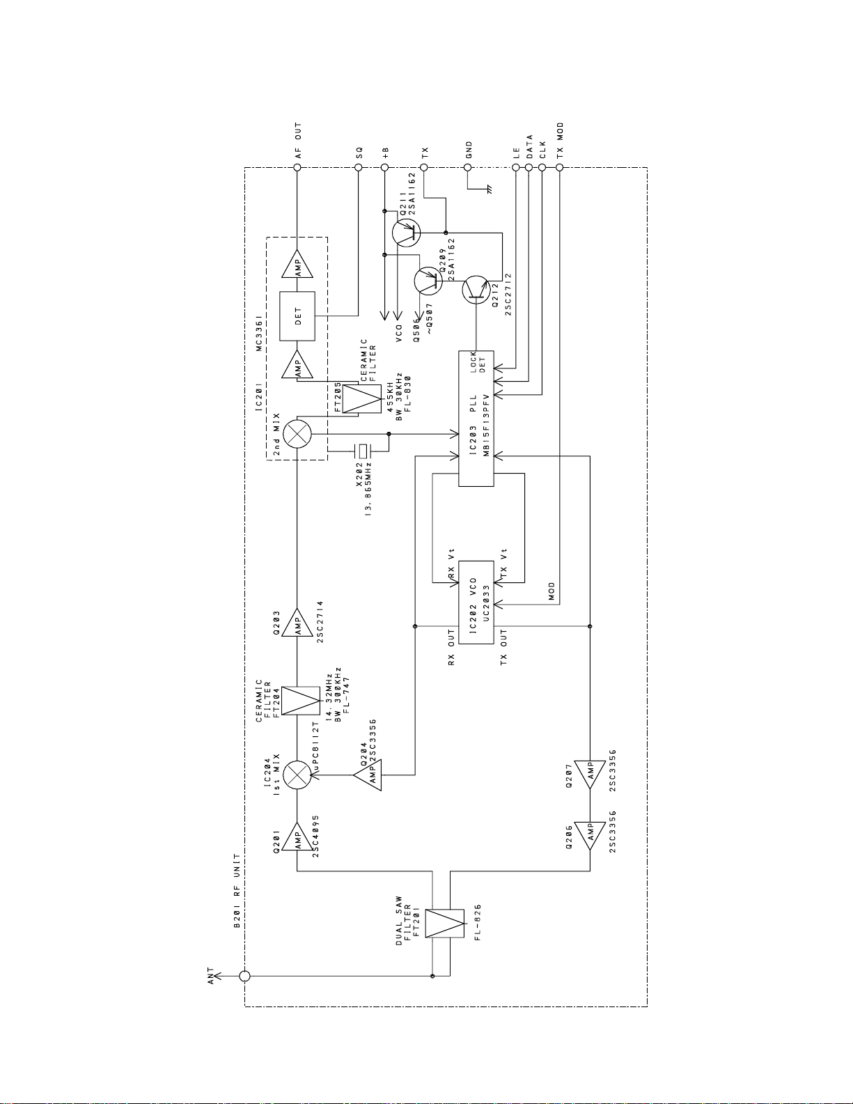
Base, RF
— 11 —
Page 13
—13—
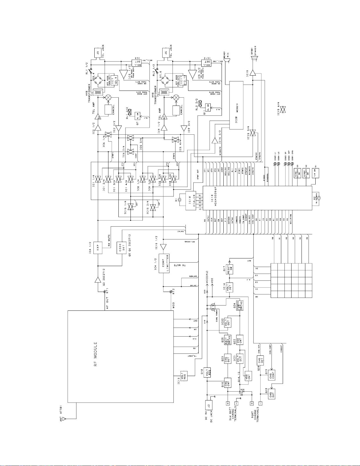
Base, Main
—12 —
Page 14
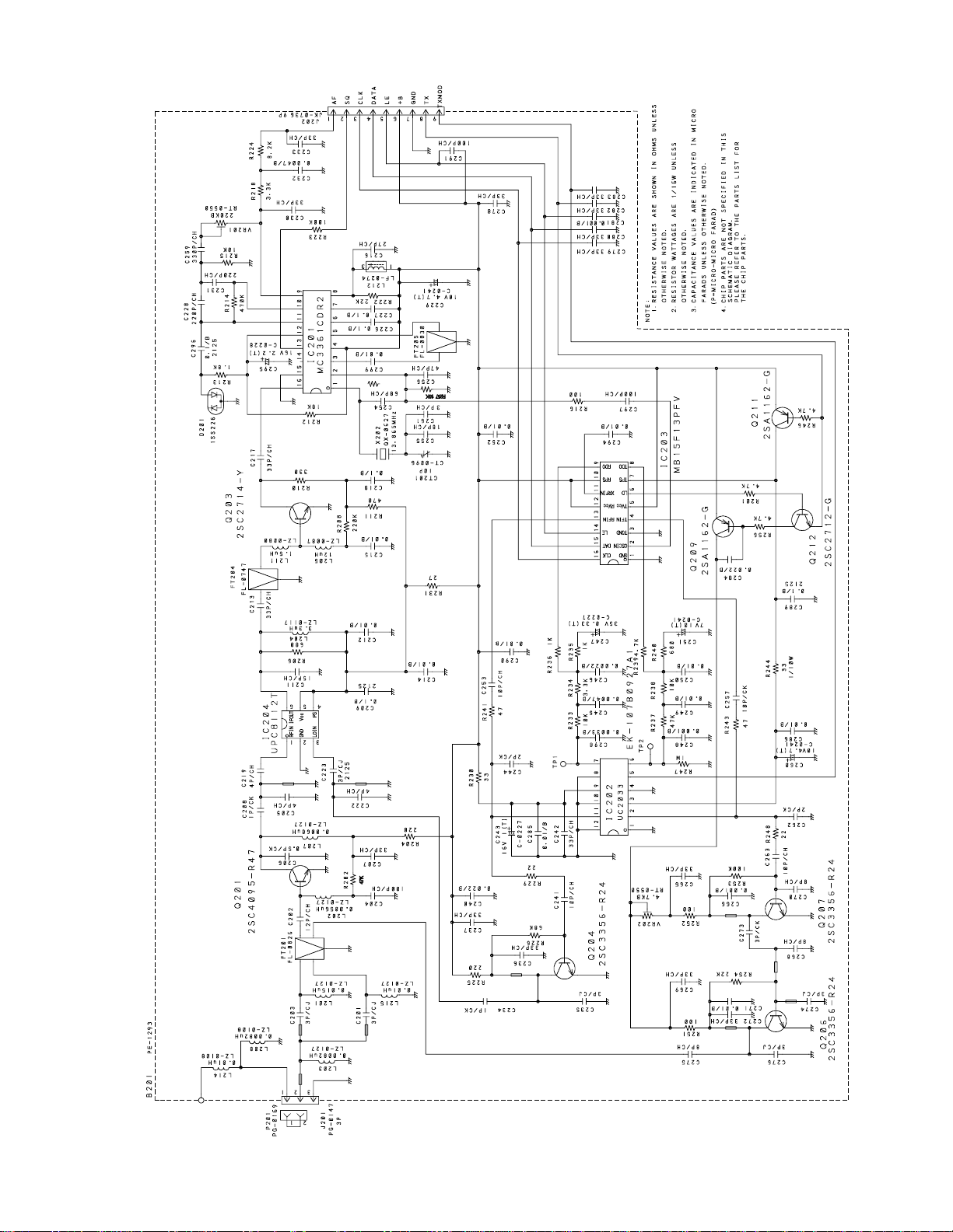
SCHEMATIC DIAGRAMS
— 15 —
— 14 —
Page 15
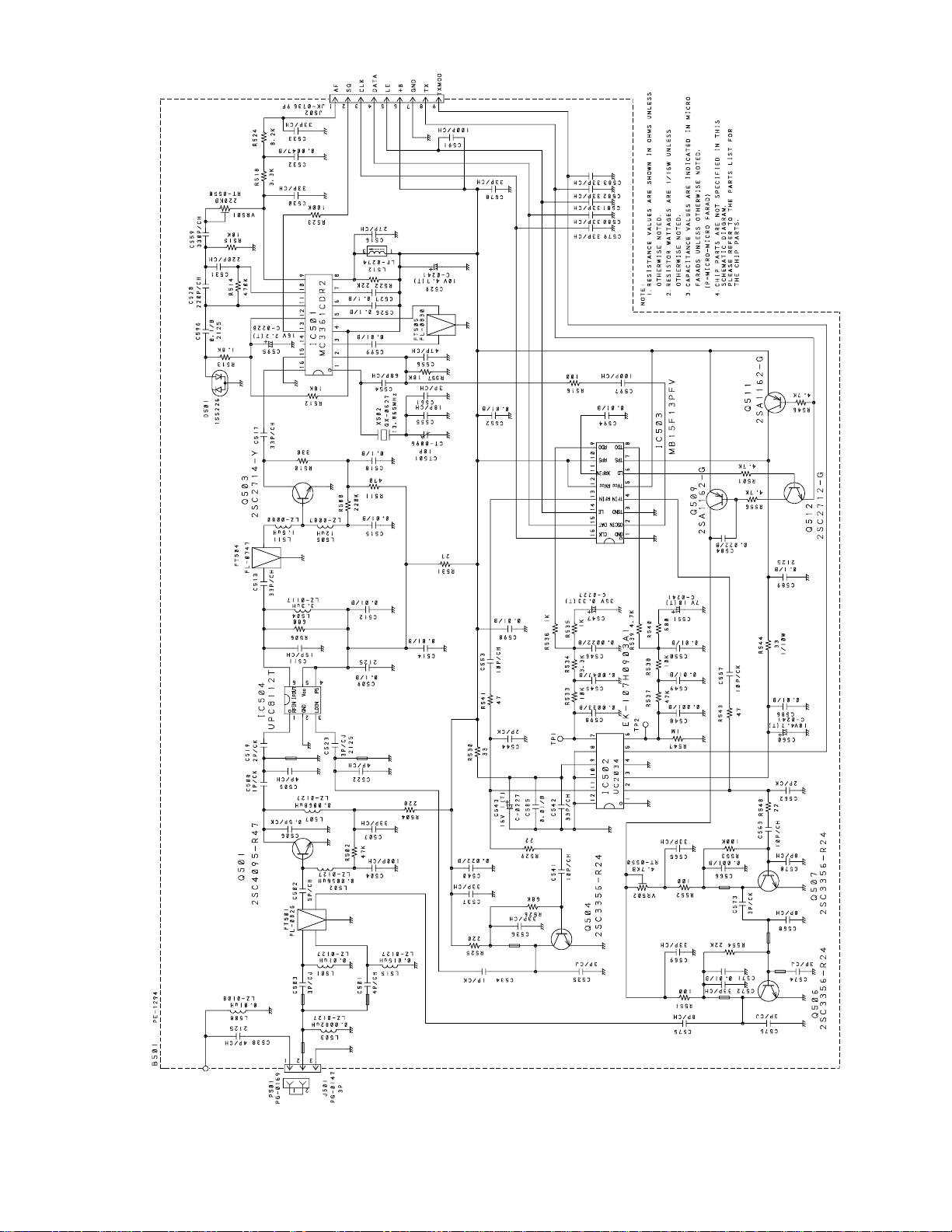
— 17 —
Base, RF
— 16 —
Page 16
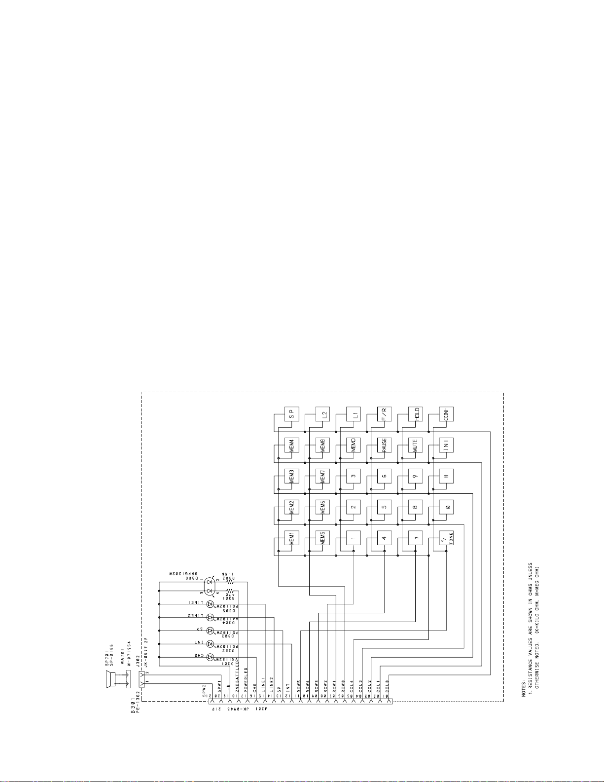
—19—
Base, Key
—18 —
Page 17
— 21 —
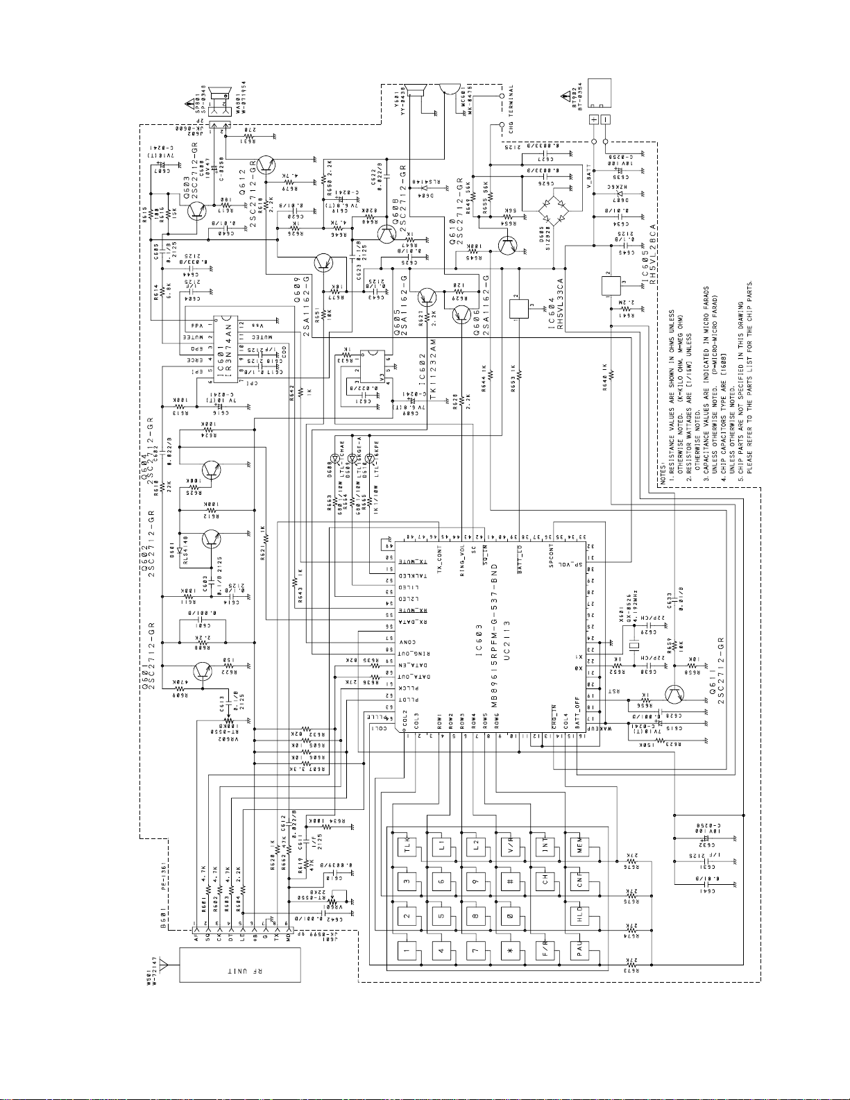
Handset, Main
— 20 —
Page 18
— 23 —
Handset, RF
— 22 —
Page 19

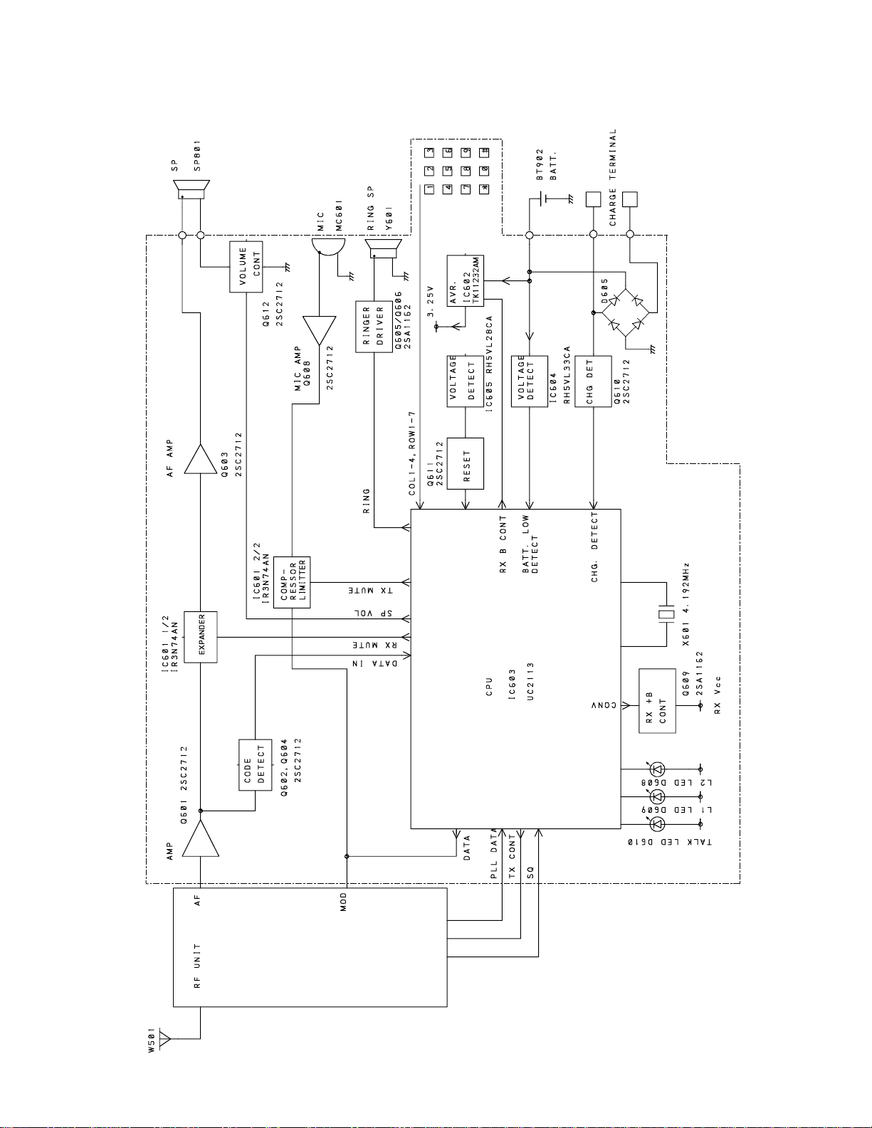
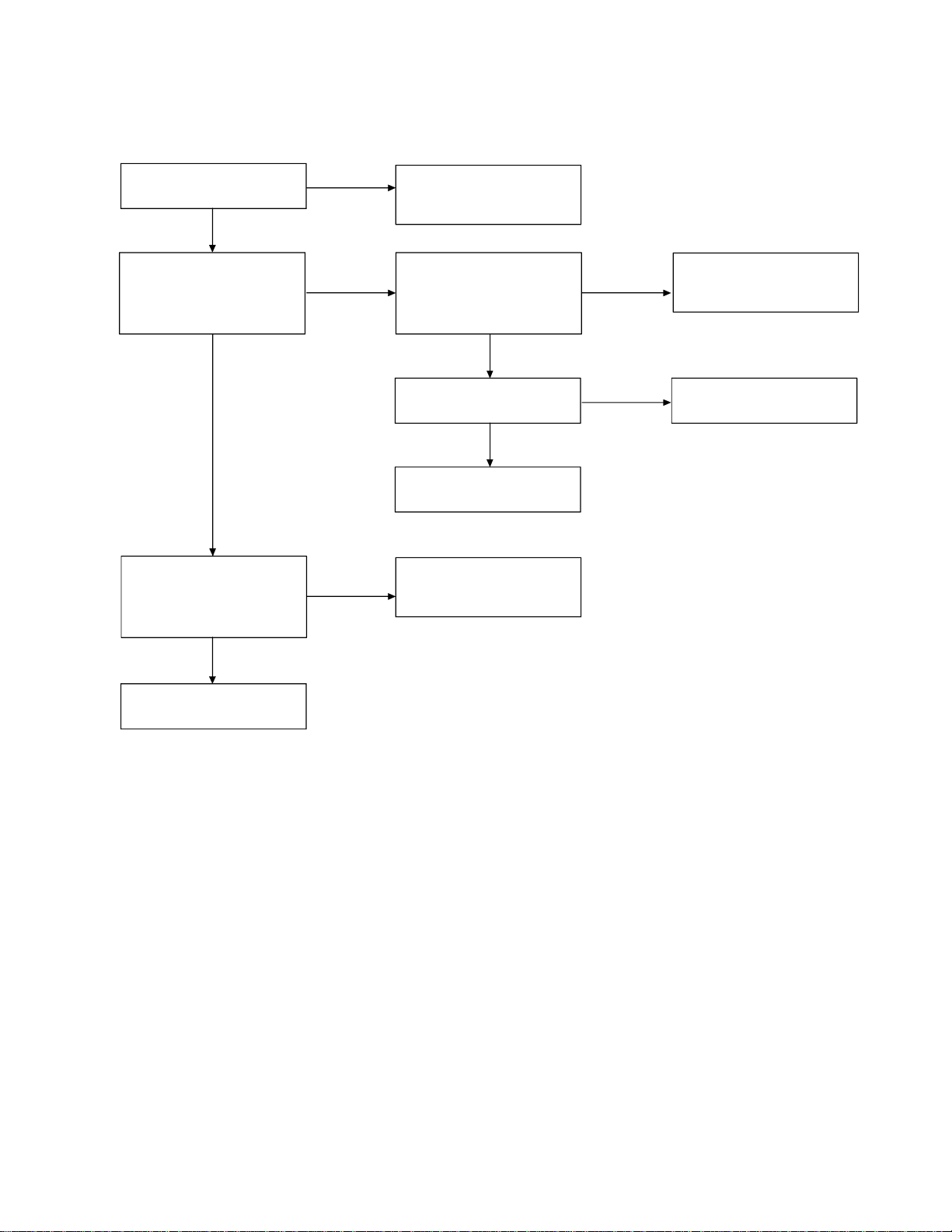
TROUBLESHOOTING HINTS
1. The bell does not ring.
When the INTCOM key of
the base is pressed, does
the ringer on the handset
ring?
OK
When the TEL SG is joined
with the base to make bell
signal, is there pulse wave
at Pin 4 of IC3 (Line 1) or
IC12 (Line 2)?
OK
Is there pulse wave at
Pin 62 (Line 1) or 55 (Line 2)
of IC18?
OK
Check IC18 and its
peripheral circuit.
NG
NG
NG
See 2. The bell does not
ring & page does not ring.
Check IC3 (Line 1) or
IC12 (Line 2) and TEL network
circuit.
Check R42, R80, R399 and
C51 (Line 1) or R122, R152,
R396 and C88 (Line 2).
— 24 —
Page 20
2. The bell does not ring & page does not ring.
Can the base and handset
be connec ted?
OK
Press handset DIAL key
while in TALK MODE.
Can key touch sound be
heard from the ringer?
OK
When the INTCOM key of
the base is pr essed, does
Pin 8 of J1 change from
high to low?
NG
NG
NG
See 3. The base and
handset cannot be
connected.
When the key of the
handset is pressed, can the
pulse output at pin 58 of
IC603 be seen?
OK
At the Q606 collector, can
the pulse wave be seen?
OK
Check RINGER Y601.
Check KEY RUBBER.
NG
NG
Check IC603.
Check R627, R629, Q605
and Q606.
OK
Check IC18 and its
peripheral circuit.
— 25 —
Page 21
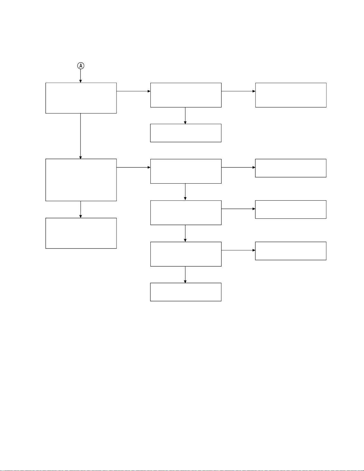
3. The base and handset cannot be connected.
Check whether the base is
able to set in the test
mode 1.
OK
Check the TX POWER and
the TX FREQUENCY on
the base unit.
OK
Set the base in the test
mode 3, check whether
deviation of the TX data is
app. 7 kHz Dev.
OK
Set the base in the test
mode 8, 902.979122 MHz
(250 Hz ±7 kHz Dev.) 1 mV
output sig nal from RF jack
is applied.
Can the INTCOM LED be
lighted?
OK
NG
NG
NG
NG
Check IC18 and its
peripheral circuit.
Check base RF unit.
Check whether there is a
250 Hz data waveform at
Pin 9 of J1.
OK
Check base RF unit.
Check whether there is a
250 Hz data waveform at
Pin 1 of J1.
OK
Check whether there is a
250 Hz data waveform at
the Q2 collector.
NG
NG
NG
Check RT2, R22, R56, R57
R58, R59 and C18.
Check base RF unit.
Check RT1, Q2 and their
peripheral circuits.
Check whether the
handset is able to set in the
test mode 1.
OK
Check the TX POWER and
the TX FREQUENCY on
the handset unit.
OK
NG
NG
OK
Check whether there is a
250 Hz data waveform at
Pin 11 of IC18.
OK
Check IC18 and its
peripheral circuit.
Check IC603 and its
peripheral circuit.
Check handset RF unit.
NG
Check Q5, Q6 and their
peripheral circuits.
— 26 —
Page 22
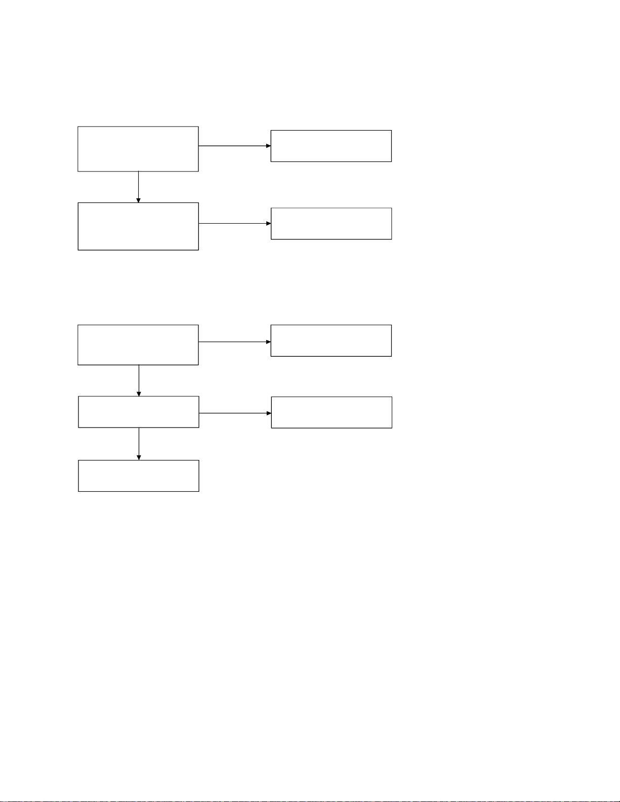
Set the handset in the test
mode 3, check whether
deviation of the TX data is
app. 7 kHz Dev.
OK
NG
Check whether there is a
250Hz data waveform at
Pin 9 of J601.
OK
Check handset RF unit.
NG
Check VR601, R619, R632,
R634, R635, R636
and C611.
Set the handset in the test
mode 6, 927.000602 MHz
(250 Hz ±7 kHz Dev.) 1mV
output signal from RF jack
is applied. Check whether
the bell ring.
OK
Place the handset on the
base to charge about
5 seconds, then connect
again.
NG
Check whether the 250 Hz
data wareform from Pin 1
of J601 is fed.
OK
Check whether there is a
250 Hz data waveform at
the Q601 collector.
OK
Check whether there is a
250 Hz data waveform at
Pin 55 of IC603.
OK
Check IC603 and its
peripheral circuit.
NG
NG
NG
Check handset RF unit.
Check VR602, Q601 and
their peripheral circuits .
Check Q602, Q604 and
their peripheral circuits .
— 27 —
Page 23
4. Will not dial out.
(TONE)
Check whether th ere is a
DTMF waveform on Pin 8
(Line 1) or Pin 4 (Line 2) of
IC6.
OK
Check whether th ere is a
DTMF waveform on Pin 7
of IC2 (Line 1) or Pin 1 of
IC11 (Line 2).
(PULSE)
Check whether th ere is a
pulse on Pin 70 (Line 1) or
Pin 69 (Line 2) of IC18.
OK
Check the collector of Q8
(Line 1) or Q11 (Line 2).
OK
NG
NG
NG
NG
Check IC10 and IC6.
Check IC2 or IC11.
Check IC18.
Check Q8 and R82 (Line 1)
or Q11 and R150 (Line 2).
Check RL1 (Line 1) or
RL2 (Line 2).
— 28 —
Page 24

5. TROUBLE WITH INTERCOM MODE
5-1. The voice from the Base unit cannot be heard on the Handset.
Check whether there is an
audio waveform on Pin 23
of IC20.
OK
Check Pin 2 of IC15.
NG
Check MC401 and IC20.
5-2. The voice from the Handset cannot be heard on the Base unit.
Check whether there is an
audio waveform on Pin 4
of IC15.
OK
Check whether there is an
audio waveform on Pin 14
of IC20.
OK
NG
NG
Check IC15.
Check IC20 and IC19.
Check W702 and SP701.
— 29 —
Page 25

6. TROUBLE WITH SPEAKERPHONE MODE
6-1. The voice of the caller cannot be heard (INCOMING CALL).
Check whether there is an
audio wavefor m on Pin 11
of IC1 (Line 1) or Pin 8 of
IC8 (Line 2).
OK
Check whether there is an
audio wavefor m on Pin 1
of IC16.
OK
Check whether there is an
audio wavefor m on Pin 14
of IC20.
OK
Check W702 and SP701.
NG
NG
NG
Check IC1 (Line 1) or IC8
(Line 2).
Check IC16, RL1 and Q8
(Line 1) or IC16, RL2 and
Q11 (Line 2).
Check IC19 and IC20.
6-2. Voice cannot be transmitted to the calling party (OUTGOING CALL).
Check whether there is an
audio waveform on Pin 23
of IC20.
OK
Check whether there is an
audio waveform on P in 2
of IC1 (Line 1) or Pin 3 of
IC 8 (Line 2).
OK
Check whether there is an
audio waveform on P in 7
of IC2 (Line 1) or Pin 1 of
IC11 (Line 2).
OK
Check Q1, T1, RL1 and Q8
(Line 1) or Q7, T2, RL2 and
Q11 (Line 2).
NG
NG
NG
Check MC401 and IC20.
Check IC1 (Line 1) or IC8
(Line 2 ) .
Check IC2 (Line 1) or IC11
(Line 2 ) .
— 30 —
Page 26

IC AND TRANSISTOR VOLTAGE CHART
Transistors Unit [V]
Ref.
Pin STBY TALK Note
No.
E 0 0.8
C 3.6 3.6Q1
B 6.0 1.5
E 0.1 0.1
Q2 C 2.0 2.0
B 0.7 0.7
E 0.7 0.8
C0 0Q3
B 0.7 0.8
E0 0
Q4 C 0 5.1
B 0.6 0
E0 0
Q5 C 0.5 0.7
B 0.5 0.5
E0 0
Q6 C 2.8 0.3
B 0.4 0.5
E 0.9 0.9
Q7 C 3.5 3.5
B 1.6 1.6
E0 0
Q8 C 5.1 0
B 0 0.8
E0 0
Q9 C0 0
B 0.6 0.6
E 5.9 6.0
Q10 C 10.8 10.0
B 6.5 6.5
E0 0
Q11 C 5.1 5.1
B0 0
E0 0
Q12 C0 0
B 0.6 0.6
E 0.7 0.7
Q13 C0 0
B 0.7 0.7
E 10.0 9.7
Q14 C 5.1 5.1
B 10.0 9.7
E0 0
Q15 C 10.0 9.7
B0 0
E 10.8 10.3
Q16 C 10.8 10.3
B 10.0 9.6
Ref.
Pin STBY TALK Note
No.
E0 0
Q17 C 4.9 4.9
B0 0
E0 0
Q18 C0 0
B 0.7 0.7
E0 0
Q19 C0 0
B 0.7 0.7
E0 0
Q20 C 5.0 4.9
B0 0
E0 0
Q21 C 1.9 1.9
B0 0
E 00
Q22 C0 0
B 0.6 0.6
E 11.2 10.7
Q23 C 00
B 11.0 10.5
E 00
Q24 C 00
B 0.7 0.7
E 00
Q25 C 3.8 3.7
B 00
E0 0
Q201 C 2.67 2.66
B 0.80 0.70
E0 0
Q203 C 2.23 2.22
B 0.71 0.67
E0 0
Q204 C 2.70 2.69
B 0.73 0.73
E0 0
Q206 C 0 2.42
B 0 0.77
E0 0
Q207 C 0 1.52
B 0 0.71
E 3.26 3.25
Q209 C 0.29 3.19
B 2.82 2.54
E 3.26 3.25
Q211 C 0 3.20
B 2.81 2.54
Unit [V]
— 31 —
Page 27

Unit [V]
Ref.
Pin STBY TALK Note
No.
E 2.81 1.04
Q212 C 2.84 1.05
B 3.25 1.71
E0 0
Q501 C 2.60/0 2.60 INTERMITTENT(STBY)
B 0.54/0 0.80 INTERMITTENT(STBY)
E0 0
Q503 C 2.10/0 2.13 INTERMITTENT(STBY)
B 0.62/0 0.71 INTERMITTENT(STBY)
E0 0
Q504 C 2.70/0 2.61 INTERMITTENT(STBY)
B 0.60/0 0.73 INTERMITTENT(STBY)
E0 0
Q506 C 0 2.40
B 0 0.77
E0 0
Q507 C 0 2.42
B 0 0.73
E 3.20/0 3.21 INTERMITTENT(STBY)
Q509 C 0.18 3.14
B 2.70/0 2.50 INTERMITTENT(STBY)
E 3.20/0 3.21 INTERMITTENT(STBY)
Q511 C 0 3.21
B 2.50/0.20 2.51 INTERMITTENT(STBY)
E 2.70/0 1.02 INTERMITTENT(STBY)
Q512 C 2.70/0 1.02 INTERMITTENT(STBY)
B 3.19/0 1.68 INTERMITTENT(STBY)
E 0 1.7
Q601 C 0 1.7
B 0 1.7
E0 0
Q602 C 0 0.5
B 0 0.5
E 0 1.6
Q603 C 0 2.6
B 0 2.2
E0 0
Q604 C 0 1.5
B 0 1.4
E 3.6 3.6
Q605 C0 0
B 3.6 3.6
E0 0
Q606 C0 0
B 3.6 3.6
E 0 0.3
Q608 C 0 1.8
B 0 0.9
Ref.
Pin STBY TALK Note
No.
E 3.6 3.6
Q609 C 0 3.5
B 3.6 2.9
E0 0
Q610 C 3.6 3.6
B0 0
E0 0
Q611 C 3.6 3.6
B0 0
E0 0
Q612 C0 0
B0 0
Unit [V]
— 32 —
Page 28

IC’S Unit [V]
Ref.
Pin STBY TALK Note
No.
1 0.8 0.8
20 0
3 0 1.1
4 1.2 1.2
5 0 4.8
6 0 4.8
IC1 70 0
8 2.1 2.1
9 0 2.0
10 2.1 2.1
11 0 0
12 0 0
13 0 0
14 5.1 5.1
1 2.1 2.1
2 2.1 2.1
3 2.1 2.1
40 0
IC2
5 2.1 2.1
6 2.1 2.1
7 2.1 2.1
8 5.1 5.1
1 0.7 0.9
2 0.7 0.9
IC3
30 0
4 3.2 3.2
1 5.1 5.1
2 0 3.8
3 1.2 1.2
4 0.9 0.6
5 1.2 1.2
6 1.2 1.2
IC4 7 1.2 1.2
8 1.2 1.2
9 0.6 0.7
10 1.2 1.2
11 0 3.8
12 0 0
1 1.6 1.6
2 1.6 1.6
3 1.5 1.5
40 0
IC5
5 1.5 1.5
6 1.6 1.6
7 1.6 1.6
8 3.2 3.2
1 2.1 2.1
20 0
IC6
3 5.1 5.1
40 0
Ref.
Pin STBY TALK Note
No.
50 0
60 0
70 0
80 0
9 5.1 5.1
IC6
10 0 0
11 2.1 2.1
12 0 0
13 0 0
14 5.1 5.1
10 0
2 0.6 0.7
IC7
30 0
4 0.6 0.6
1 1.2 1.2
20 0
30 0
4 0.6 0.6
50 0
60 0
IC8 70 0
80 0
9 2.1 2.1
10 0 0
11 2.1 2.1
12 0 0
13 0 0
14 5.1 5.1
1 5.1 5
2 0 5.1
3 5.1 0
4 5.1 5.1
5 0 5.1
6 5.1 0
7 4.7 5.1
IC10 8 0 4.7
90 0
10 0 0
11 0 0
12 0 0
13 0 0
14 5.1 5.1
1 2.1 2.1
2 2.1 2.1
3 2.1 2.1
40 0
IC11 5 2.1 2.1
6 2.1 2.1
7 2.1 2.1
8 5.1 5.1
Unit [V]
— 33 —
Page 29

Ref.
Pin STBY TALK Note
No.
1 0.7 0.7
IC12
IC13
IC14 2 5.1 5.1
IC15 8 0.3 0.3
IC16
IC17
IC18 70 0
2 0.8 0.8
30 0
4 5.1 5.1
1 5.1 5.1
20 0
3 1.2 1.2
4 3.2 3.2
50 0
6 5.1 5.1
1 5.1 5.1
30 0
1 1.0 1.0
20 0
3 1.3 1.2
40 0
50 0
60 0
70 0
9 0.2 0.2
10 0.6 0.6
11 5.1 5.1
12 0 0
13 0 0
14 5.1 5.1
1 2.1 2.1
2 2.1 2.1
3 2.1 2.1
40 0
5 2.1 2.1
6 2.1 2.1
7 2.1 2.1
8 5.1 5.1
1 0.2 0.2
2 0.6 0.6
30 0
4 0.6 0.6
10 0
20 0
30 0
40 0
50 0
6 0 4.8
80 0
90 0
10 0 4.7
11 2.6 0.3
12 0 0
Unit [V]
Ref.
Pin STBY TALK Note
No.
13 0 4.8
14 0 5.1
15 0 0
16 0 0
17 0 0
18 4.8 0
19 0 0
20 1.0 1.0
21 4.8 4.8
22 4.8 4.8
23 4.8 0~4.8
24 4.8 4.8
25 4.8 4.8
26 4.8 4.8
27 0 0
28 0 0
29 0 0
30 0 0
31 0 0
32 0 0
33 0 0
34 5.1 5.1
35 5.1 5.1
36 5.1 5.1
37 5.1 5.1
38 5.1 5.1
IC18 39 0 0
40 0 0
41 0 0
42 0 0
43 0 0
44 4.8 4.8
45 4.8 4.8
46 2.3 2.3
47 4.8 4.8
48 4.8 4.8
49 4.8 4.8
50 0 0
51 2.3 2.3
52 2.2 2.1
53 4.8 4.8
54 5.1 5.1
55 5.1 5.1
56 0 0
57 0.6 0
58 0 0
59 1.6 1.6
60 1.6 1.6
61 1.6 1.6
62 3.2 3.2
63 0 0
Unit [V]
— 34 —
Page 30

Ref.
Pin STBY TALK Note
No.
64 3.2/0 3.2/0 TONE/PULSE
65 0 0 RING OFF
66 0 0 RING OFF
67 3.2 3.2 TONE/PULSE
68 3.2 3.2
69 0 0
70 0 4.8
71 0 0
IC18 72 4.8 4.8
73 4.6 4.6
74 5.1 5.1
75 4.8 4.8
76 4.8 4.8
77 4.8 4.8
78 0 0
79 0 0
80 0 0
1 4.7 4.8
2 2.1 2.1
3 2.0 2.0
IC19
IC20
4 2.0 2.0
5 1.9 2.0
6 5.1 5.1
70 0
8 1.9 2.0
1 2.2 2.2
2 2.1 2.1
3 5.0 5.0
4 0.8 0.8
5 2.2 2.2
6 2.1 2.1
7 2.1 2.1
8 4.4 4.5
90 0
10 5.0 5.0
11 1.4 1.4
12 2.3 2.3
13 0 0
14 1.6 1.6
15 0.6 0.6
16 0.6 0.6
17 0.4 0.4
18 4.7 4.8
19 1.9 2.0
20 4.4 4.5
21 4.4 4.5
22 4.4 4.5
23 0.7 0.7
24 5.1 5.1
Unit [V]
Ref.
Pin STBY TALK Note
No.
1 9.3 8.8
IC21
IC22 2 6.0 6.0
IC201
IC202
IC203
2 10.2 9.7
30 0
1 5.8 5.8
30 0
1 3.21 3.21
2 2.68 2.68
3 2.78 2.78
4 3.26 3.25
5 2.85 2.84
6 2.85 2.84
7 2.85 2.84
8 3.26 3.25
9 0.87 0.92
10 0.63 0.63
11 0.67 0.67
12 0.64 0.74
13 3.16 0
14 0 0
15 0 0
16 3.26 3.25
10 0
20 0
3 0 2.99
40 0
50 0
6 0 1.60
7 1.54 1.50
80 0
9 3.05 3.04
10 0 0
11 0 0
12 0 0
10 0
2 1.31 1.32
30 0
4 2.62 2.22
5 3.26 3.25
6 3.20 3.20
7 0 3.25
8 0 1.74
9 1.53 1.54
10 3.25 3.25
11 2.23 2.23
12 3.26 3.25
13 2.23 2.23
14 0 0
15 DATA DATA
16 CLK CLK
Unit [V]
— 35 —
Page 31

Ref.
Pin STBY TALK Note
No.
1 1.17 1.17
20 0
IC204
IC501
IC502
IC503
IC504 20 0
3 1.37 1.37
4 3.02 3.01
5 3.02 3.01
6 3.02 3.01
1 3.12/0 3.17 INTERMITTENT(STBY)
2 2.60/0.10 2.64 INTERMITTENT(STBY)
3 2.60/0 2.71 INTERMITTENT(STBY)
4 3.21/0 3.21 INTERMITTENT(STBY)
5 2.80/0 2.78 INTERMITTENT(STBY)
6 2.70/0 2.78 INTERMITTENT(STBY)
7 2.70/0 2.78 INTERMITTENT(STBY)
8 3.21/0 3.21 INTERMITTENT(STBY)
9 1.01/0 1.07 INTERMITTENT(STBY)
10 0.45/0 0.63 INTERMITTENT(STBY)
11 0.65/0 0.67 INTERMITTENT(STBY)
12 0.42/0 0.74 INTERMITTENT(STBY)
13 3.00/0 0 INTERMITTENT(STBY)
14 0.80/0.30 0.80 INTERMITTENT(STBY)
15 0 0
16 3.21/0 3.21 INTERMITTENT(STBY)
10 0
20 0
3 0 2.98
40 0
50 0
6 0 1.64
7 1.50/0.40 1.58 INTERMITTENT(STBY)
80 0
9 3.00/0 3.01 INTERMITTENT(STBY)
10 0 0
11 0 0
12 0 0
10 0
2 1.20/0 1.26 INTERMITTENT(STBY)
30 0
4 2.60/0 2.19 INTERMITTENT(STBY)
5 3.21/0 3.21 INTERMITTENT(STBY)
6 3.00/0 3.15 INTERMITTENT(STBY)
7 0 3.17
8 0 1.66
9 1.50/0.40 1.51 INTERMITTENT(STBY)
10 3.21/0 3.21 INTERMITTENT(STBY)
11 2.20/0 2.19 INTERMITTENT(STBY)
12 3.21/0 3.21 INTERMITTENT(STBY)
13 2.12/0 2.19 INTERMITTENT(STBY)
14 0 0
15 DATA/0 DATA INTERMITTENT(STBY)
16 CLK/0 CLK INTERMITTENT(STBY)
1 1.19/0 1.19 INTERMITTENT(STBY)
3 1.35/0 1.37 INTERMITTENT(STBY)
Unit [V]
Ref.
Pin STBY TALK Note
No.
3 1.35/0 1.37 INTERMITTENT(STBY)
IC504
IC601 7 0.2 1.3
IC602
IC603 14 3.6 3.6
4 2.95/0 2.98 INTERMITTENT(STBY)
5 2.95/0 2.98 INTERMITTENT(STBY)
6 2.93/0 2.97 INTERMITTENT(STBY)
1 0 3.5
2 0 2.9
3 0.2 1.3
4 0.2 1.0
5 0 1.2
6 0 1.3
8 0.2 0.2
9 0 0.6
10 0.2 1.3
11 0 2.9
12 0.2 0.3
1 0 3.5
20 0
3 0 1.2
4 0 3.3
50 0
6 3.6 3.6
1 3.6 3.6
2 3.6 3.6
3 0.2 0
40 0
50 0
60 0
70 0
80 0
90 0
10 0 0
11 3.6 3.6
12 0 0
13 0 0
15 3.6 3.6
16 3.6 3.6
17 0 3.6
18 0 0
19 3.6 3.6
20 0 0
21 0 0
22 0.2 1.4
23 3.6 1.6
24 0 0
25 0 0
26 0 0
27 0 0
28 0 0
29 0 0
Unit [V]
— 36 —
Page 32

Ref.
Pin STBY TALK Note
No.
30 0 0
31 0 0
32 0 0
33 0 0
34 0 0
35 0 3.6
36 0 0
37 0 0
38 3.6 3.6
39 0 0
40 0 0
41 0 3.1
42 0 3.6
43 3.6 3.6
44 0 0
45 0 0
46 0 0
IC603
IC604 2 3.6 3.6
IC605 2 3.6 3.6
47 0 0
48 0 0
49 0 0
50 0 3.5
51 3.6 0
52 3.6 0
53 3.6 3.6
54 0 3.5
55 0 1.5
56 3.6 3.6
57 3.6 0
58 3.6 3.6
59 0 0
60 0 1.2
61 0 0
62 0 0
63 0 0
64 3.6 3.6
1 3.6 3.6
30 0
1 3.6 3.6
30 0
Unit [V]
— 37 —
Page 33

Base Unit
e
SEMICONDUCTOR LEAD IDENTIFICATION
D1/D11: MTZ36AJ
D2/D6/D10/D12/D14
D17/D18/D25/D26/D27: 1N4148
D5/D20: HZ33CP
D15: 1N4003
D22: HZ7A1
D29/D30: HZ6C-3
Cathode
D306: BRPG1202W
Anode
D9:RLS4148
D28: RLZJ-6.2B
Anode
Cathode
Cathode
Q1/Q2/Q4/Q5/Q6/Q7/Q8/Q9/Q11
/Q12/Q15/Q17/Q19/Q20/Q21/Q22
/Q24/Q25/Q212: 2SC2712
Q3/Q13/Q23/Q209/Q211: 2SA1162
Q203: 2SC2714
Q204/Q206/Q207: 2SC3356
C
B: Base
BE
E: Emitter
C: Collector
D3/D4/D7/D8
D201: 1SS226
Anode/Cathode
Anode Cathode
Anode
Q10: 2SD1683
D1683
B: Base
C: Collector
C
E
E: Emitter
B
D23: RB160L-40
Cathode
D301: VR1102W
D302/D303/D305: PG1102W
D304: AA1102W
Cathode
Anode
D31: HZK6C
Cathode
Anode
Q14: 2SB1118
ECB
B: Base
C: Collector
E: Emitter
Anod
Q16: 2SA950
B: Base
C
B
E: Emitter
C: Collector
E
Q18: 2SD471
E
C
B
Q201: 2SC4095
BE
EC
— 38 —
IC1/IC6/IC8/IC15
TC4066BF
Vss
1
2
3
4
5
6
7
IN/OUT1
OUT/IN1
OUT/IN2
IN/OUT2
CONT2
CONT3
14
13
12
11
10
9
8
VDD
CONT1
CONT4
IN/OUT4
OUT/IN4
OUT/IN3
IN/OUT3
Page 34

IC2/IC11/IC16
M5223L
IC3/IC7/IC12/IC17
LTV-817
IC4
IR3N74AN
IC5
NJU7032M
8
1
IC14: RH5VL33CA
IC21: RH5VL35CA
IC22: RH5VL47CA
1
IC19
MC34119D
CD
1
Vin
2
3
4
FC2
FC1
IC20
MC33219AP
24
XDI
TLI
VB
CT
CD
NC
RLI
1
23
2
3
22
21
4
5
20
6
19
7
18
8
17
9
16
15
10
11
14
12
13
CP2
CPT
TLO
CPR
RLO
1
2
4
3
Vcc
MUTE
EREC
EPI
VREF
EO
1
2
3
4
5
6
12
11
10
GND
MUTE
CO
CREC
9
ACP
8
CPI
7
OUT1
IN–1
IN+1
GND
8
1
+
–
2
+
3
4
V
DD
OUT2
7
–
6
IN–2
IN+2
5
IC18
HD6433033
P72/AN2
P73/AN3
P74/AN4
P75/AN5
P76/AN6
P77/AN7
Vref
AVcc
P80 IRO0
P81 IRO1
P82 IRO2
P83 IRO3
PA0/TP0\TCLKA
PA1/TP1\TCLKB
PA2/TP2\TIOCA0/TCLKC
PA3/TP3\TIOCB0/TCLKD
A23/PA4/TP4/TIOCA1
A22/PA5/TP5/TIOCB1
A21/PA6/TP6/TIOCA2
A20/PA7/TP7/TIOCB2
80 79 78 77 76 75 74 73 72 71 70 69 68 67 66 65 64 63 62 61
3
2
VO2
8
GND
7
Vcc
6
VO1
5
Vcc
TAO
TAI
MCO
MCI
VLC
MUTE
RXI
RXO
RAI
RAO
GND
IC201
MC3361CDR2
Crystal
Osc.
Mixer
Output
Vcc
Limiter
Input
Decoupling
Quad
Input
1
2
3
4
5
6
7
8
TIOCA3/TP8/PB0
TIOCB3/TP9/PB1
TIOCA4/TP10/PB2
TIOCB4/TP11/PB3
TOCXA4/TP12/PB4
TOCXB4/TP13/PB5
TP14/PB6
ADTRG/TP15/PB7
IRQ4/SCK/P94
Mixer
16
Input
15
GND
Audio
14
Mute
Scan
13
Control
Squelch
12
Input
Filter
11
Output
Filter
10
Input
Demodulator
9
Audio
TXD/P90
RXD/P92
Vss
D0/P30
D1/P31
D2/P32
D3/P33
D4/P34
D5/P35
D6/P36
D7/P37
1
2
3
4
5
6
7
8
9
10
11
12
13
14
15
16
17
18
19
20
21 22 23 24 25 26 27 28 29 30 31 32 33 34 35 36 37 38 39 40
Vcc
A0/P10
A1/P11
A2/P12
A3/P13
A4/P14
A5/P15
A6/P16
Vss
A7/P17
A8/P20
A9/P21
A10/P22
A11/P23
IC202
EK-107
TX Vt
1
2
3
4
5
6
TX GND
TX OUT
TX Vcc
TX GND
TX MOD
A13/P25
A12/P24
A14/P26
A15/P27
A16/P50
A17/P51
12
11
10
9
8
7
P71/AN1
60
P70/AN0
59
58
AVss
57
RESO
P65 WR
56
P64 HD
55
54
P63 A5
53
Vcc
52
XTAL
EXTAL
51
50
Vss
49
NMI
48
RES
47
STBY
f
46
45
MD1
44
MD0
43
P60WAIT
42
P53/A19
41
P52/A18
RX GND
RX OUT
RX GND
RX Vcc
RX GND
RX Vt
— 39 —
Page 35

D
IC203
MB15F13PFV1
IC204
µPC8112T
IC 1 0
TC 35219F
IC 1 3
TK 11232AM
GND
RX
1
OSC
IN
2
GND
TX
3
fin
TX
4
Vcc
TX
5
LD/fout
6
PS
TX
7
Do
TX
8
Handset
D501: 1SS226
Anode/Cathode
C2K
PS
Vcc
IF out
DD
V
TD
−
CONT1
CONT2
Vss
OSCout
OSCin
1
2
3
4
5
6
7
TO N E
14
PS
−
13
12
DATA1
11
DATA2
10
DATA3
9
DATA4
8
MUTE
D605: S1ZB20
CONT
GND
NO ISE BYPASS
1
2
3
6
5
4
D608: LTL-1CHAE
D609: LTL-16KGE
V
IN
GND
V
OUT
Clock
16
Data
15
LE
14
fin
13
Vcc
12
Xfin
11
PS
10
D
9
Lo in
GND
RF in
RX
RX
RX
RX
ORX
D601/D604: RLS4148
D607: RLZJ-6.2B
D610: LTL-16KPE
+
Cathode
Anode
−
Anode Cathode
Q501: 2SC4095
BE
EC
IC501
MC3361CDR2
Osc.
Mixer
Output
Vcc
Limiter
Input
Quad
Input
1
2
3
4
5
6
7
8
Crystal
ecoupling
Mixer
16
Input
15
GND
Audio
14
Mute
Scan
13
Control
Squelch
12
Input
Filter
11
Output
Filter
10
Input
Demodulator
9
Audio
Q503: 2SC2714
Q504/Q506/Q507: 2SC3356
Q512/Q601/Q602/Q603/Q604
/Q608/Q610/Q611/Q612: 2SC2712
Q509/Q511/Q605
/Q606/Q609: 2SA1162
IC502
EK-107
1
TX GND
2
TX OUT
3
TX Vcc
4
TX GND
5
TX MOD
6
TX Vt
~
~
Anode
Cathode
C
B: Base
E: Emitter
C: Collector
E
B
12
RX GND
11
RX OUT
10
RX GND
9
RX Vcc
8
RX GND
RX Vt
7
— 40 —
Page 36

E
C
IC503
MB15F13PFV1
IC504
µPC8112T
IC601
IR3N74AN
GND
RX
OSC
IN
GND
TX
fin
TX
Vcc
TX
LD/fout
PS
TX
Do
TX
IC602
TK11232AM
CONT
GND
NOISE BYPASS
IC605
RH5VL28CA
IC604
RH5VL33CA
Clock
1
2
3
4
5
6
7
8
1
2
34
16
Data
15
LE
14
fin
RX
13
Vcc
RX
12
Xfin
RX
11
PS
RX
10
Do
RX
9
Vin
6
5
Vout
Lo in
GND
C2K
RF in
IC603
MB89615RPFM
P46/SO2
P47/SI2
P50/AN0
P51/AN1
P52/AN2
P53/AN3
P54/AN4
P55/AN5
P56/AN6
P57/AN7
AV cc
AVR
AV ss
P60/INTO
P61/INT1
P62/INT2
PS
Vcc
IF out
P45/SCK2
P44/BZ
P43
P42
P41
P40
P37/PTO
P36/WTO
V cc
646362616059585756555453525150
1
2
3
4
5
6
7
8
9
10
11
12
13
14
15
16
171819202122232425262728293031
Vcc
MUTE
EO
EREC
EPI
VREF
P35/PWC
P34/EC
P33/SI1
1
2
3
4
5
6
P32/SO1
P31/SCK1
P30/ADST
V ss
49
48
47
46
45
44
43
42
41
40
39
38
37
36
35
34
33
32
GND
12
MUT
11
CO
10
CRE
9
ACP
8
CPI
7
P00/AD0
P01/AD1
P02/AD2
P03/AD3
P04/AD4
P05/AD5
P06/AD6
P07/AD7
P10/A08
P11/A09
P12/A10
P13/A11
P14/A12
P15/A13
P16/A14
P17/A15
X0
MOD0
MOD1
X1
V ss
P27/ALE
P26/RD
P25/WR
P24/CLK
P21/HAK
P23/RDY
P22/HRQ
P20/BUFC
3
2
1
P64
RST
P63/INT3
— 41 —
Page 37

Base, Main
ELECTRICAL PARTS LOCATIONS
— 42 —
Page 38

Base, RF
— 43 —
Page 39

Base, Key
— 44 —
Page 40

Handset, Main
— 45 —
Page 41

Handset, RF
— 46 —
Page 42

Base
WIRING DIAGRAMS
—47 —
Page 43

Handset
—48 —
Page 44

EXPLODED VIEW AND MECHANICAL PARTS LIST
Base, Unit
31
5
22
22
13
16
5
20
18
1
19
10
26
23
17
4
11
12
9
22
24
25
22
22
30
28
22
2
8
15
3
24
7
7
Note:
To remove the RF Assembly from the unit, remove four screws
Three screws
23
are used for fastening the Shield Cases 26 and 27 .
14
22
24
27
21
29
.
— 49 —
Page 45

Base Unit
LOC.
NO.
10 RC005684 GCAS457909Z Hook ABS 1
11 RC005687 KDPZ457907Z Index Cover PC 1
12 RC005693 PLBM457759Z Index Paper 1
13 RC005690 LNBZ357883Z Key Rubber SI 1
14 RC005124 GNBZ455306Z Knob, Slide ABS 1
15 RC005694 PLBS458142Z Label, ID 1
16 RC005329 PLBZ456718Z Label, Indication 1
17 RC005695 PLBZ458144Z Label, Indication 1
18 RC005681 GCAS357877Z LED Lens PMMA 1
19 RC005682 GCAS357878Z LED Lens PMMA 1
20 RC005683 GCAS357879Z LED Lens PMMA 1
21 RC005688 KDPZ457908Z Plate, Display PC 1
22 RC000941 SSCW802608N Screw, P Tight Bind HD + D2.6X8 NI 26
23 RC004893 SSCW802612N Screw, P Tight Bind HD + D2.6X12 NI 3
24 RC004028 SSCW802616N Screw, P Tight Bind HD + D2.6X16 NI 8
25 RC001752 SSCW283012N Screw, Tapping Bind+& SP Washer D3X12 NI 1
26 RC005263 GSDC255851Z Shield Case ABS 1
27 RC005264 GSDC255852Z Shield Case ABS 1
28 RC005691 NSPZ457885Z Spring Terminal SWP 2
29 RC005679 GCAS257876Z Stand ABS 1
30 RC005692 NSPZ457886Z Torsion Spring SWP 1
31 RC005696 RUTC457032Z Wool Coated Paper, Wool Tack 2
PART NO. REF. NO. DESCRIPTION QTY
1 RC005685 GNBZ157880Z Button, Function ABS 1
2 RC005680 GCAS257882Z Case, Battery ABS 1
3 RC005678 GCAS157875Z Case, Bottom ABS 1
4 RC005677 GCAS157874Z Case, Top ABS 1
5 RC005686 HTML457884Z Charge Terminal C5191(PBP) 2
7 RC002384 LFUT428079Z Foot Bum pon SJ-5916 1.6T 4
8 RC005689 LHDZ453179Z Holder, Mic CR 1
9 RC005444 HHDS431080Z Holder, Speaker SUS304-CSP,0.6T 1
— 50 —
Page 46

Handset
58
67
64
72
67
56
67
68
59
55
51
69
70
71
52
61
53
65
66
Note:
To remove the RF Assembly from the unit, remove four screws
Three screws
68
are used for fastening the Shield Cases 70 and 71 .
63
67
69
62
60
54
57
.
— 51 —
Page 47

Handset
LOC.
NO.
51 RC006714 RBLD457881Z Blind PC 1
52 RC006705 GNBZ357892Z Button, Function ABS 1
53 RC006706 GNBZ457891Z Button, Push ABS 1
54 RC005700 GCAS157887Z Case, Front ABS 1
55 RC006701 GCAS157888Z Case, Rear ABS 1
56 RC006707 HTML457893Z Charge Terminal C2680(BSP) 2
57 RC006703 GCAS457897Z Cover Elastomer 1
58 RC006702 GCAS357889Z Cover, Battery ABS 1
59 RC006715 RCUM417955Z Cushion Moltplene 1
60 RC004286 RCUN451209Z Cushion Neoprene 1
61 RC006709 LHDZ456969Z Holder, Mic EPDM 1
62 RC006704 GHDZ357890Z Holder, Speaker ABS 1
63 RC006710 LNBZ357895Z Key Rubber SI 1
64 RC006713 PLBZ458086Z Label, Caution 1
65 RC006712 PLBS458143Z Label, ID 1
66 RC006708 KDPZ457896Z Plate, Display PMMA 1
67 RC000941 SSCW802608N Screw, P Tight Bind HD + D2.6X8 NI 8
68 RC004893 SSCW802612N Screw, P Tight Bind HD + D2.6X12 NI 3
69 RC004028 SSCW802616N Screw, P Tight Bind HD + D2.6X16 NI 4
70 RC005263 GSDC255851Z Shield Case ABS 1
71 RC005264 GSDC255852Z Shield Case ABS 1
72 RC006711 NSPZ457894Z Spring Terminal SWP 2
PART NO. REF. NO. DESCRIPTION QTY
— 52 —
Page 48

PARTS LIST
0.5
PRODUCT SAFETY NOTE: Products marked with a have special characteristics important to safety.
Before replacing any of these components, read carefully the product safety notice of this service manual.
Don
’ t degrade the safety of the product through important servicing.
Symbol F G J K M N Z P Symbol C D
% ±1 ±2 ±5 ±10 ±20 ±30 −20+80 0+100 pF ±0.25 ±
LOC.
NO.
CAPACITORS
The following codes indicate variation of capacitors against temperatures,:
YA = ±5%, YB = ±10%, YD = +20 −30%, YE = +20 −50% ( −25 ~ +85 °C), ZF = +30 −80%, (−10 ~ +79 °C),
CH = 0
SL = +350 ppm/°C ~ −1000 ppm/°C, UJ = −750 ppm/°C ±120 ppm/°C, CJ = 0 ± 120ppm/°C, CK = 0 ± 250ppm/°C
C1 RC004491 BCUA816804Z CERAMIC 68PF 50V J CH
C2 RC004500 BCUB812235Z CERAMIC 0.022UF 50V K B
C3 RC001795 BCAZ112216Z ELECTROLYTIC 220UF 10V M C-156
C4 RC004500 BCUB812235Z CERAMIC 0.022UF 50V K B
C6 RC004970 BCUB811525Z CERAMIC 0.0015UF 50V K B
C7 RC004593 BCUA818214Z CERAMIC 820PF 50V J CH
C8 RC004494 BCUB511045Z CERAMIC 0.1UF 25V K B
C9 RC004494 BCUB511045Z CERAMIC 0.1UF 25V K B
C10 RC004739 BCUB813335Z CERAMIC 0.033UF 50V K B
C11 RC000777 BCZY0120001 SEMI-CONDUCTOR 0.022UF 18V CZ-120
C12 RC000752 BCKB821025Z CERAMIC 0.001UF 500V K YB(B)
C13 RC002204 BCQL525645Z MYLAR 0.56UF 250V K C-167
C14 RC004496 BCUB811025Z CERAMIC 0.001UF 50V K B
C15 RC005635 BCKB134715Z CERAMIC 470PF 1000V K YB(B)
C16 RC004560 BCUB813325Z CERAMIC 0.0033UF 50V K B
C17 RC004494 BCUB511045Z CERAMIC 0.1UF 25V K B
C18 RC005166 BCUP311050Z CERAMIC 1UF 16V Z F
C19 RC004497 BCUB811035Z CERAMIC 0.01UF 50V K B
C20 RC004494 BCUB511045Z CERAMIC 0.1UF 25V K B
C21 RC001802 BCAZ314706Z ELECTROLYTIC 47UF 16V M C-156
C22 RC005166 BCUP311050Z CERAMIC 1UF 16V Z F
C23 RC004494 BCUB511045Z CERAMIC 0.1UF 25V K B
C24 RC005166 BCUP311050Z CERAMIC 1UF 16V Z F
C25 RC004608 BCUB312245Z CERAMIC 0.22UF 16V K B
C27 RC004497 BCUB811035Z CERAMIC 0.01UF 50V K B
C28 RC004497 BCUB811035Z CERAMIC 0.01UF 50V K B
C29 RC004497 BCUB811035Z CERAMIC 0.01UF 50V K B
C30 RC004560 BCUB813325Z CERAMIC 0.0033UF 50V K B
C31 RC004487 BCUA814704Z CERAMIC 47PF 50V J CH
C32 RC004138 BCAZ811006Z ELECTROLYTIC 10UF 50V M C-156
C33 RC001794 BCAZ111016Z ELECTROLYTIC 100UF 10V M C-156
C34 RC001805 BCAZ811096Z ELECTROLYTIC 1UF 50V M C-156
C35 RC004562 BCUB814725Z CERAMIC 0.0047UF 50V K B
PART NO.
±60 ppm/°C, TH = −470 ppm/°C, ±60ppm/°C, B = ±10%, F = +30 −80%,
REF
NO.
DESCRIPTION
— 53 —
Page 49

LOC.
NO.
PART NO.
REF
NO.
DESCRIPTION
C36 RC004562 BCUB814725Z CERAMIC 0.0047UF 50V K B
C37 RC005667 BCUB811835Z CERAMIC 0.018UF 50V K B
C38 RC005667 BCUB811835Z CERAMIC 0.018UF 50V K B
C39 RC005635 BCKB134715Z CERAMIC 470PF 1000V K YB(B)
C40 RC004494 BCUB511045Z CERAMIC 0.1UF 25V K B
C41 RC004503 BCUP512240Z CERAMIC 0.22UF 25V Z F
C42 RC004138 BCAZ811006Z ELECTROLYTIC 10UF 50V M C-156
C43 RC004496 BCUB811025Z CERAMIC 0.001UF 50V K B
C44 RC004737 BCUA815614Z CERAMIC 560PF 50V J CH
C45 RC004501 BCUB812735Z CERAMIC 0.027UF 50V K B
C46 RC004497 BCUB811035Z CERAMIC 0.01UF 50V K B
C47 RC004500 BCUB812235Z CERAMIC 0.022UF 50V K B
C49 RC004970 BCUB811525Z CERAMIC 0.0015UF 50V K B
C50 RC004593 BCUA818214Z CERAMIC 820PF 50V J CH
C51 RC004739 BCUB813335Z CERAMIC 0.033UF 50V K B
C52 RC004494 BCUB511045Z CERAMIC 0.1UF 25V K B
C53 RC004167 BCAZ511016Z ELECTROLYTIC 100UF 25V M C-156
C54 RC005166 BCUP311050Z CERAMIC 1UF 16V Z F
C55 RC002204 BCQL525645Z MYLAR 0.56UF 250V K C-167
C56 RC004494 BCUB511045Z CERAMIC 0.1UF 25V K B
C57 RC004494 BCUB511045Z CERAMIC 0.1UF 25V K B
C58 RC004955 BCFD852240Z ELECTRIC DOUBLE LAYER 0.22F 5.5V Z C-266
C59 RC005635 BCKB134715Z CERAMIC 470PF 1000V K YB(B)
C60 RC005635 BCKB134715Z CERAMIC 470PF 1000V K YB(B)
C61 RC004478 BCUA811014Z CERAMIC 100PF 50V J CH
C62 RC004481 BCUA811514Z CERAMIC 150PF 50V J CH
C63 RC004497 BCUB811035Z CERAMIC 0.01UF 50V K B
C64 RC004560 BCUB813325Z CERAMIC 0.0033UF 50V K B
C65 RC004970 BCUB811525Z CERAMIC 0.0015UF 50V K B
C66 RC004487 BCUA814704Z CERAMIC 47PF 50V J CH
C67 RC004494 BCUB511045Z CERAMIC 0.1UF 25V K B
C68 RC004739 BCUB813335Z CERAMIC 0.033UF 50V K B
C69 RC000777 BCZY0120001 SEMI-CONDUCTOR 0.022UF 18V CZ-120
C70 RC001794 BCAZ111016Z ELECTROLYTIC 100UF 10V M C-156
C71 RC000752 BCKB821025Z CERAMIC 0.001UF 500V K YB(B)
C72 RC004496 BCUB811025Z CERAMIC 0.001UF 50V K B
C73 RC004496 BCUB811025Z CERAMIC 0.001UF 50V K B
C74 RC001794 BCAZ111016Z ELECTROLYTIC 100UF 10V M C-156
C75 RC004500 BCUB812235Z CERAMIC 0.022UF 50V K B
C76 RC004496 BCUB811025Z CERAMIC 0.001UF 50V K B
C77 RC004445 BCAZ903316Z ELECTROLYTIC 330UF 6.3V M C-156
C78 RC004497 BCUB811035Z CERAMIC 0.01UF 50V K B
C79 RC004445 BCAZ903316Z ELECTROLYTIC 330UF 6.3V M C-156
C80 RC004508 BCXC311050Z CERAMIC 1UF 16V Z F
C81 RC004480 BCUA811504Z CERAMIC 15PF 50V J CH
C82 RC004480 BCUA811504Z CERAMIC 15PF 50V J CH
— 54 —
Page 50

LOC.
NO.
PART NO.
REF
NO.
DESCRIPTION
C83 RC004481 BCUA811514Z CERAMIC 150PF 50V J CH
C84 RC004560 BCUB813325Z CERAMIC 0.0033UF 50V K B
C85 RC004560 BCUB813325Z CERAMIC 0.0033UF 50V K B
C86 RC004492 BCUA818204Z CERAMIC 82PF 50V J CH
C87 RC004138 BCAZ811006Z ELECTROLYTIC 10UF 50V M C-156
C88 RC004739 BCUB813335Z CERAMIC 0.033UF 50V K B
C89 RC001805 BCAZ811096Z ELECTROLYTIC 1UF 50V M C-156
C90 RC004167 BCAZ511016Z ELECTROLYTIC 100UF 25V M C-156
C91 RC004562 BCUB814725Z CERAMIC 0.0047UF 50V K B
C92 RC004562 BCUB814725Z CERAMIC 0.0047UF 50V K B
C93 RC004494 BCUB511045Z CERAMIC 0.1UF 25V K B
C94 RC005667 BCUB811835Z CERAMIC 0.018UF 50V K B
C95 RC004494 BCUB511045Z CERAMIC 0.1UF 25V K B
C96 RC005667 BCUB811835Z CERAMIC 0.018UF 50V K B
C97 RC004497 BCUB811035Z CERAMIC 0.01UF 50V K B
C98 RC004167 BCAZ511016Z ELECTROLYTIC 100UF 25V M C-156
C99 RC004497 BCUB811035Z CERAMIC 0.01UF 50V K B
C100 RC002651 BCAZ312216Z ELECTROLYTIC 220UF 16V M C-156
C101 RC004497 BCUB811035Z CERAMIC 0.01UF 50V K B
C102 RC001794 BCAZ111016Z ELECTROLYTIC 100UF 10V M C-156
C103 RC004497 BCUB811035Z CERAMIC 0.01UF 50V K B
C104 RC004496 BCUB811025Z CERAMIC 0.001UF 50V K B
C105 RC004608 BCUB312245Z CERAMIC 0.22UF 16V K B
C106 RC004608 BCUB312245Z CERAMIC 0.22UF 16V K B
C107 RC004494 BCUB511045Z CERAMIC 0.1UF 25V K B
C108 RC004494 BCUB511045Z CERAMIC 0.1UF 25V K B
C109 RC004138 BCAZ811006Z ELECTROLYTIC 10UF 50V M C-156
C110 RC001805 BCAZ811096Z ELECTROLYTIC 1UF 50V M C-156
C111 RC005134 BCUA812714Z CERAMIC 270PF 50V J CH
C112 RC001802 BCAZ314706Z ELECTROLYTIC 47UF 16V M C-156
C113 RC004494 BCUB511045Z CERAMIC 0.1UF 25V K B
C114 RC004562 BCUB814725Z CERAMIC 0.0047UF 50V K B
C115 RC004562 BCUB814725Z CERAMIC 0.0047UF 50V K B
C116 RC005166 BCUP311050Z CERAMIC 1UF 16V Z F
C117 RC005166 BCUP311050Z CERAMIC 1UF 16V Z F
C118 RC004497 BCUB811035Z CERAMIC 0.01UF 50V K B
C119 RC001794 BCAZ111016Z ELECTROLYTIC 100UF 10V M C-156
C120 RC004497 BCUB811035Z CERAMIC 0.01UF 50V K B
C121 RC004496 BCUB811025Z CERAMIC 0.001UF 50V K B
C122 RC004497 BCUB811035Z CERAMIC 0.01UF 50V K B
C123 RC004138 BCAZ811006Z ELECTROLYTIC 10UF 50V M C-156
C124 RC004494 BCUB511045Z CERAMIC 0.1UF 25V K B
C125 RC001795 BCAZ112216Z ELECTROLYTIC 220UF 10V M C-156
C126 RC004494 BCUB511045Z CERAMIC 0.1UF 25V K B
C127 RC005166 BCUP311050Z CERAMIC 1UF 16V Z F
C128 RC004494 BCUB511045Z CERAMIC 0.1UF 25V K B
— 55 —
Page 51

LOC.
NO.
PART NO.
REF
NO.
DESCRIPTION
C129 RC001807 BCAZ812296Z ELECTROLYTIC 2.2UF 50V M C-156
C130 RC001794 BCAZ111016Z ELECTROLYTIC 100UF 10V M C-156
C131 RC005166 BCUP311050Z CERAMIC 1UF 16V Z F
C132 RC004497 BCUB811035Z CERAMIC 0.01UF 50V K B
C133 RC001794 BCAZ111016Z ELECTROLYTIC 100UF 10V M C-156
C134 RC004145 BCAZ812206Z ELECTROLYTIC 22UF 50V M C-156
C135 RC001794 BCAZ111016Z ELECTROLYTIC 100UF 10V M C-156
C136 RC005166 BCUP311050Z CERAMIC 1UF 16V Z F
C137 RC004502 BCUB814735Z CERAMIC 0.047UF 50V K B
C138 RC004494 BCUB511045Z CERAMIC 0.1UF 25V K B
C139 RC004494 BCUB511045Z CERAMIC 0.1UF 25V K B
C140 RC004497 BCUB811035Z CERAMIC 0.01UF 50V K B
C141 RC005166 BCUP311050Z CERAMIC 1UF 16V Z F
C142 RC004445 BCAZ903316Z ELECTROLYTIC 330UF 6.3V M C-156
C143 RC004496 BCUB811025Z CERAMIC 0.001UF 50V K B
C144 RC005183 BCUC811091Z CERAMIC 1PF 50V C CK
C145 RC005183 BCUC811091Z CERAMIC 1PF 50V C CK
C146 RC005183 BCUC811091Z CERAMIC 1PF 50V C CK
C147 RC005183 BCUC811091Z CERAMIC 1PF 50V C CK
C148 RC000777 BCZY0120001 SEMI-CONDUCTOR 0.022UF 18V CZ-120
C149 RC004496 BCUB811025Z CERAMIC 0.001UF 50V K B
C150 RC004497 BCUB811035Z CERAMIC 0.01UF 50V K B
C151 RC005183 BCUC811091Z CERAMIC 1PF 50V C CK
C152 RC001800 BCAZ311016Z ELECTROLYTIC 100UF 16V M C-156
C153 RC004741 BCUP811040Z CERAMIC 0.1UF 50V Z F
C201 RC005224 BCMT813091Z CERAMIC 3PF 50V C CJ
C202 RC005211 BCMM811204Z CERAMIC 12PF 50V J CH
C203 RC005224 BCMT813091Z CERAMIC 3PF 50V C CJ
C204 RC005210 BCMM811014Z CERAMIC 100PF 50V J CH
C205 RC005218 BCMM814091Z CERAMIC 4PF 50V C CH
C206 RC005290 BCMS815081Z CERAMIC 0.5PF 50V C CK
C207 RC005216 BCMM813304Z CERAMIC 33PF 50V J CH
C208 RC005222 BCMS811091Z CERAMIC 1PF 50V C CK
C209 RC002229 BCXT511045Z CERAMIC 0.1UF 25V K B
C211 RC005212 BCMM811504Z CERAMIC 15PF 50V J CH
C212 RC005205 BCML811035Z CERAMIC 0.01UF 50V K B
C213 RC005216 BCMM813304Z CERAMIC 33PF 50V J CH
C214 RC005205 BCML811035Z CERAMIC 0.01UF 50V K B
C215 RC005205 BCML811035Z CERAMIC 0.01UF 50V K B
C216 RC005215 BCMM812704Z CERAMIC 27PF 50V J CH
C217 RC005216 BCMM813304Z CERAMIC 33PF 50V J CH
C218 RC005202 BCML311045Z CERAMIC 0.1UF 16V K B
C219 RC005218 BCMM814091Z CERAMIC 4PF 50V C CH
C222 RC005218 BCMM814091Z CERAMIC 4PF 50V C CH
C223 RC003998 BCBJ813091Z CERAMIC 3PF 50V C CJ
C226 RC005202 BCML311045Z CERAMIC 0.1UF 16V K B
— 56 —
Page 52

LOC.
NO.
PART NO.
REF
NO.
DESCRIPTION
C227 RC005202 BCML311045Z CERAMIC 0.1UF 16V K B
C228 RC005214 BCMM812214Z CERAMIC 220PF 50V J CH
C229 RC005225 BCSS114796Z TANTALUM CHIP TAPE 4.7UF 10V M A C-241
C230 RC005216 BCMM813304Z CERAMIC 33PF 50V J CH
C231 RC005214 BCMM812214Z CERAMIC 220PF 50V J CH
C232 RC005208 BCML814725Z CERAMIC 0.0047UF 50V K B
C233 RC005216 BCMM813304Z CERAMIC 33PF 50V J CH
C234 RC005222 BCMS811091Z CERAMIC 1PF 50V C CK
C235 RC005224 BCMT813091Z CERAMIC 3PF 50V C CJ
C236 RC005216 BCMM813304Z CERAMIC 33PF 50V J CH
C237 RC005216 BCMM813304Z CERAMIC 33PF 50V J CH
C240 RC005203 BCML512235Z CERAMIC 0.022UF 25V K B
C241 RC005209 BCMM811002Z CERAMIC 10PF 50V D CH
C242 RC005216 BCMM813304Z CERAMIC 33PF 50V J CH
C243 RC004861 BCPP311096Z TANTALUM CHIP TAPE 1UF 16V M A C-227
C244 RC005223 BCMS812091Z CERAMIC 2PF 50V C CK
C245 RC005208 BCML814725Z CERAMIC 0.0047UF 50V K B
C246 RC005206 BCML812225Z CERAMIC 0.0022UF 50V K B
C247 RC004862 BCPP663386Z TANTALUM CHIP TAPE 0.33UF 35V M A C-227
C248 RC005204 BCML811025Z CERAMIC 0.001UF 50V K B
C249 RC005205 BCML811035Z CERAMIC 0.01UF 50V K B
C250 RC005205 BCML811035Z CERAMIC 0.01UF 50V K B
C251 RC004185 BCSS951006Z TANTALUM CHIP TAPE 10UF 7V M A C-241
C252 RC005205 BCML811035Z CERAMIC 0.01UF 50V K B
C253 RC005209 BCMM811002Z CERAMIC 10PF 50V D CH
C254 RC005220 BCMM816804Z CERAMIC 68PF 50V J CH
C255 RC005213 BCMM811804Z CERAMIC 18PF 50V J CH
C256 RC005219 BCMM814704Z CERAMIC 47PF 50V J CH
C257 RC005209 BCMM811002Z CERAMIC 10PF 50V D CH
C259 RC005217 BCMM813314Z CERAMIC 330PF 50V J CH
C260 RC005225 BCSS114796Z TANTALUM CHIP TAPE 4.7UF 10V M A C-241
C261 RC005224 BCMT813091Z CERAMIC 3PF 50V C CJ
C262 RC005223 BCMS812091Z CERAMIC 2PF 50V C CK
C263 RC005209 BCMM811002Z CERAMIC 10PF 50V D CH
C265 RC005216 BCMM813304Z CERAMIC 33PF 50V J CH
C266 RC005204 BCML811025Z CERAMIC 0.001UF 50V K B
C268 RC005221 BCMM818092Z CERAMIC 8PF 50V D CH
C269 RC005216 BCMM813304Z CERAMIC 33PF 50V J CH
C270 RC005221 BCMM818092Z CERAMIC 8PF 50V D CH
C271 RC005205 BCML811035Z CERAMIC 0.01UF 50V K B
C272 RC005216 BCMM813304Z CERAMIC 33PF 50V J CH
C273 RC005224 BCMT813091Z CERAMIC 3PF 50V C CJ
C274 RC005224 BCMT813091Z CERAMIC 3PF 50V C CJ
C275 RC005221 BCMM818092Z CERAMIC 8PF 50V D CH
C276 RC005224 BCMT813091Z CERAMIC 3PF 50V C CJ
C278 RC005216 BCMM813304Z CERAMIC 33PF 50V J CH
— 57 —
Page 53

LOC.
NO.
PART NO.
REF
NO.
DESCRIPTION
C279 RC005216 BCMM813304Z CERAMIC 33PF 50V J CH
C280 RC005216 BCMM813304Z CERAMIC 33PF 50V J CH
C281 RC005204 BCML811025Z CERAMIC 0.001UF 50V K B
C282 RC005216 BCMM813304Z CERAMIC 33PF 50V J CH
C283 RC005216 BCMM813304Z CERAMIC 33PF 50V J CH
C284 RC005203 BCML512235Z CERAMIC 0.022UF 25V K B
C285 RC005205 BCML811035Z CERAMIC 0.01UF 50V K B
C286 RC005205 BCML811035Z CERAMIC 0.01UF 50V K B
C289 RC002229 BCXT511045Z CERAMIC 0.1UF 25V K B
C290 RC005205 BCML811035Z CERAMIC 0.01UF 50V K B
C291 RC005210 BCMM811014Z CERAMIC 100PF 50V J CH
C294 RC005205 BCML811035Z CERAMIC 0.01UF 50V K B
C295 RC003287 BCPT312296Z TANTALUM CHIP TAPE 2.2UF 16V M A C-228
C296 RC002229 BCXT511045Z CERAMIC 0.1UF 25V K B
C297 RC005210 BCMM811014Z CERAMIC 100PF 50V J CH
C298 RC005207 BCML813325Z CERAMIC 0.0033UF 50V K B
C299 RC005205 BCML811035Z CERAMIC 0.01UF 50V K B
C501 RC004990 BCUH814091Z CERAMIC 4PF 50V C CH
C502 RC004992 BCUH815091Z CERAMIC 5PF 50V C CH
C503 RC004980 BCUG813091Z CERAMIC 3PF 50V C CJ
C504 RC004982 BCUH811014Z CERAMIC 100PF 50V J CH
C505 RC004990 BCUH814091Z CERAMIC 4PF 50V C CH
C506 RC008736 BCUF815081Z CERAMIC 0.5PF 50V C CK
C507 RC004988 BCUH813304Z CERAMIC 33PF 50V J CH
C508 RC004978 BCUF811091Z CERAMIC 1PF 50V C CK
C509 RC004494 BCUB511045Z CERAMIC 0.1UF 25V K B
C511 RC004984 BCUH811504Z CERAMIC 15PF 50V J CH
C512 RC004998 BCUL811035Z CERAMIC 0.01UF 50V K B
C513 RC004988 BCUH813304Z CERAMIC 33PF 50V J CH
C514 RC004998 BCUL811035Z CERAMIC 0.01UF 50V K B
C515 RC004998 BCUL811035Z CERAMIC 0.01UF 50V K B
C516 RC004987 BCUH812704Z CERAMIC 27PF 50V J CH
C517 RC004988 BCUH813304Z CERAMIC 33PF 50V J CH
C518 RC005202 BCML311045Z CERAMIC 0.1UF 16V K B
C519 RC004979 BCUF812091Z CERAMIC 2PF 50V C CK
C522 RC004990 BCUH814091Z CERAMIC 4PF 50V C CH
C523 RC004740 BCUE813091Z CERAMIC 3PF 50V C CJ
C526 RC005202 BCML311045Z CERAMIC 0.1UF 16V K B
C527 RC005202 BCML311045Z CERAMIC 0.1UF 16V K B
C528 RC004986 BCUH812214Z CERAMIC 220PF 50V J CH
C529 RC005225 BCSS114796Z TANTALUM CHIP TAPE 4.7UF 10V M A C-241
C530 RC004988 BCUH813304Z CERAMIC 33PF 50V J CH
C531 RC004986 BCUH812214Z CERAMIC 220PF 50V J CH
C532 RC005001 BCUL814725Z CERAMIC 0.0047UF 50V K B
C533 RC004988 BCUH813304Z CERAMIC 33PF 50V J CH
C534 RC004978 BCUF811091Z CERAMIC 1PF 50V C CK
— 58 —
Page 54

LOC.
NO.
PART NO.
REF
NO.
DESCRIPTION
C535 RC004980 BCUG813091Z CERAMIC 3PF 50V C CJ
C536 RC004988 BCUH813304Z CERAMIC 33PF 50V J CH
C537 RC004988 BCUH813304Z CERAMIC 33PF 50V J CH
C538 RC004486 BCUA814091Z CERAMIC 4PF 50V C CH
C540 RC004996 BCUL512235Z CERAMIC 0.022UF 25V K B
C541 RC004981 BCUH811002Z CERAMIC 10PF 50V D CH
C542 RC004988 BCUH813304Z CERAMIC 33PF 50V J CH
C543 RC004861 BCPP311096Z TANTALUM CHIP TAPE 1UF 16V M A C-227
C544 RC004979 BCUF812091Z CERAMIC 2PF 50V C CK
C545 RC005001 BCUL814725Z CERAMIC 0.0047UF 50V K B
C546 RC004999 BCUL812225Z CERAMIC 0.0022UF 50V K B
C547 RC004862 BCPP663386Z TANTALUM CHIP TAPE 0.33UF 35V M A C-227
C548 RC004997 BCUL811025Z CERAMIC 0.001UF 50V K B
C549 RC004998 BCUL811035Z CERAMIC 0.01UF 50V K B
C550 RC004998 BCUL811035Z CERAMIC 0.01UF 50V K B
C551 RC004185 BCSS951006Z TANTALUM CHIP TAPE 10UF 7V M A C-241
C552 RC004998 BCUL811035Z CERAMIC 0.01UF 50V K B
C553 RC004981 BCUH811002Z CERAMIC 10PF 50V D CH
C554 RC004994 BCUH816804Z CERAMIC 68PF 50V J CH
C555 RC008737 BCUH811804Z CERAMIC 18PF 50V J CH
C556 RC004991 BCUH814704Z CERAMIC 47PF 50V J CH
C557 RC004981 BCUH811002Z CERAMIC 10PF 50V D CH
C559 RC004989 BCUH813314Z CERAMIC 330PF 50V J CH
C560 RC005225 BCSS114796Z TANTALUM CHIP TAPE 4.7UF 10V M A C-241
C561 RC004980 BCUG813091Z CERAMIC 3PF 50V C CJ
C562 RC004979 BCUF812091Z CERAMIC 2PF 50V C CK
C563 RC004981 BCUH811002Z CERAMIC 10PF 50V D CH
C565 RC004988 BCUH813304Z CERAMIC 33PF 50V J CH
C566 RC004997 BCUL811025Z CERAMIC 0.001UF 50V K B
C568 RC004995 BCUH818092Z CERAMIC 8PF 50V D CH
C569 RC004988 BCUH813304Z CERAMIC 33PF 50V J CH
C570 RC004995 BCUH818092Z CERAMIC 8PF 50V D CH
C570 RC004995 BCUH818092Z CERAMIC 8PF 50V D CH
C571 RC004998 BCUL811035Z CERAMIC 0.01UF 50V K B
C572 RC004988 BCUH813304Z CERAMIC 33PF 50V J CH
C573 RC004980 BCUG813091Z CERAMIC 3PF 50V C CJ
C574 RC004980 BCUG813091Z CERAMIC 3PF 50V C CJ
C575 RC004995 BCUH818092Z CERAMIC 8PF 50V D CH
C576 RC004980 BCUG813091Z CERAMIC 3PF 50V C CJ
C578 RC004988 BCUH813304Z CERAMIC 33PF 50V J CH
C579 RC004988 BCUH813304Z CERAMIC 33PF 50V J CH
C580 RC004988 BCUH813304Z CERAMIC 33PF 50V J CH
C581 RC004988 BCUH813304Z CERAMIC 33PF 50V J CH
C582 RC004988 BCUH813304Z CERAMIC 33PF 50V J CH
C583 RC004988 BCUH813304Z CERAMIC 33PF 50V J CH
C584 RC004996 BCUL512235Z CERAMIC 0.022UF 25V K B
— 59 —
Page 55

LOC.
NO.
PART NO.
REF
NO.
DESCRIPTION
C585 RC004998 BCUL811035Z CERAMIC 0.01UF 50V K B
C586 RC004998 BCUL811035Z CERAMIC 0.01UF 50V K B
C589 RC004494 BCUB511045Z CERAMIC 0.1UF 25V K B
C590 RC004998 BCUL811035Z CERAMIC 0.01UF 50V K B
C591 RC004982 BCUH811014Z CERAMIC 100PF 50V J CH
C594 RC004998 BCUL811035Z CERAMIC 0.01UF 50V K B
C595 RC003287 BCPT312296Z TANTALUM CHIP TAPE 2.2UF 16V M A C-228
C596 RC004494 BCUB511045Z CERAMIC 0.1UF 25V K B
C597 RC004982 BCUH811014Z CERAMIC 100PF 50V J CH
C598 RC005000 BCUL813325Z CERAMIC 0.0033UF 50V K B
C599 RC004998 BCUL811035Z CERAMIC 0.01UF 50V K B
C601 RC005204 BCML811025Z CERAMIC 0.001UF 50V K B
C602 RC005203 BCML512235Z CERAMIC 0.022UF 25V K B
C603 RC002229 BCXT511045Z CERAMIC 0.1UF 25V K B
C604 RC008731 BCXK311050Z CERAMIC 1UF 16V Z F
C605 RC002229 BCXT511045Z CERAMIC 0.1UF 25V K B
C607 RC004185 BCSS951006Z TANTALUM CHIP TAPE 10UF 7V M A C-241
C608 RC004903 BCFZ114706Z ELECTROLYTIC 47UF 10V M C-258
C609 RC004448 BCSS956896Z TANTALUM CHIP TAPE 6.8UF 7V M A C-241
C610 RC005275 BCML813925Z CERAMIC 0.0039UF 50V K B
C611 RC008731 BCXK311050Z CERAMIC 1UF 16V Z F
C612 RC005203 BCML512235Z CERAMIC 0.022UF 25V K B
C613 RC002229 BCXT511045Z CERAMIC M/L 0.1UF 25V K B
C614 RC002229 BCXT511045Z CERAMIC M/L 0.1UF 25V K B
C615 RC004185 BCSS951006Z TANTALUM CHIP TAPE 10UF 7V M A C-241
C616 RC004185 BCSS951006Z TANTALUM CHIP TAPE 10UF 7V M A C-241
C617 RC002229 BCXT511045Z CERAMIC 0.1UF 25V K B
C618 RC008731 BCXK311050Z CERAMIC 1UF 16V Z F
C619 RC004448 BCSS956896Z TANTALUM CHIP TAPE 6.8UF 7V M A C-241
C620 RC005205 BCML811035Z CERAMIC 0.01UF 50V K B
C621 RC005203 BCML512235Z CERAMIC 0.022UF 25V K B
C622 RC005203 BCML512235Z CERAMIC 0.022UF 25V K B
C623 RC002229 BCXT511045Z CERAMIC 0.1UF 25V K B
C625 RC005205 BCML811035Z CERAMIC 0.01UF 50V K B
C626 RC005207 BCML813325Z CERAMIC 0.0033UF 50V K B
C628 RC005204 BCML811025Z CERAMIC 0.001UF 50V K B
C629 RC005359 BCMM812204Z CERAMIC 22PF 50V J CH
C630 RC005359 BCMM812204Z CERAMIC 22PF 50V J CH
C631 RC008731 BCXK311050Z CERAMIC 1UF 16V Z F
C632 RC004902 BCFZ111016Z ELECTROLYTIC 100UF 10V M C-258
C633 RC005205 BCML811035Z CERAMIC 0.01UF 50V K B
C634 RC005205 BCML811035Z CERAMIC 0.01UF 50V K B
C635 RC004902 BCFZ111016Z ELECTROLYTIC 100UF 10V M C-258
C640 RC005205 BCML811035Z CERAMIC 0.01UF 50V K B
C641 RC005205 BCML811035Z CERAMIC 0.01UF 50V K B
C642 RC005204 BCML811025Z CERAMIC 0.001UF 50V K B
— 60 —
Page 56

LOC.
NO.
PART NO.
REF
NO.
DESCRIPTION
C643 RC002229 BCXT511045Z CERAMIC 0.1UF 25V K B
C644 RC001632 BCXT813335Z CERAMIC 0.033UF 50V K B
C645 RC002229 BCXT511045Z CERAMIC 0.1UF 25V K B
CT201 RC005226 BCTY0096100 TRIMMER CT-096 CTZ3S10A-W1PF55
CT501 RC005226 BCTY0096100 TRIMMER CT-096 CTZ3S10A-W1PF55
DIODES
D1 RC003995 BDAY0736004 ZENER MTZ36AJ T77
D2 RC002236 BDAY0246003 AXIAL 1N4148 T-77
D3 RC001635 BDAY0274001 DIODE 1SS226 TE85L
D4 RC001635 BDAY0274001 DIODE 1SS226 TE85L
D5 RC003194 BDAY0272010 ZENER HZ33CP
D6 RC002236 BDAY0246003 AXIAL 1N4148 T-77
D7 RC001635 BDAY0274001 DIODE 1SS226 TE85L
D8 RC001635 BDAY0274001 DIODE 1SS226 TE85L
D9 RC001826 BDAY0433001 DIODE RLS4148 TE11
D10 RC002236 BDAY0246003 AXIAL 1N4148 T-77
D11 RC003995 BDAY0736004 ZENER MTZ36AJ T77
D12 RC002236 BDAY0246003 AXIAL 1N4148 T-77
D14 RC002236 BDAY0246003 AXIAL 1N4148 T-77
D15 RC000781 BDAY0133001 DIODE 1N4003
D17 RC002236 BDAY0246003 AXIAL 1N4148 T-77
D18 RC002236 BDAY0246003 AXIAL 1N4148 T-77
D20 RC003194 BDAY0272010 ZENER HZ33CP
D22 RC003196 BDAY0492025 ZENER HZ7A1 TD
D23 RC008726 BDAY1019001 DIODE RB160L-40 TE25
D25 RC002236 BDAY0246003 AXIAL 1N4148 T-77
D26 RC002236 BDAY0246003 AXIAL 1N4148 T-77
D27 RC002236 BDAY0246003 AXIAL 1N4148 T-77
D28 RC003994 BDAY0671003 ZENER RLZJ-6.2B TE-11
D29 RC002471 BDAY0492045 ZENER HZ6C3 TD
D30 RC002471 BDAY0492045 ZENER HZ6C3 TD
D31 RC003195 BDAY0432004 ZENER HZK6C TR
D201 RC001635 BDAY0274001 DIODE 1SS226 TE85L
D301 RC002241 BDAY0597001 LED VR1102W-TR
D302 RC005060 BDAY0598001 LED PG1102W-TR
D303 RC005060 BDAY0598001 LED PG1102W-TR
D304 RC005638 BDAY0816001 LED AA1102W-TR
D305 RC005060 BDAY0598001 LED PG1102W-TR
D306 RC008729 BDAY0824001 LED BRPG1202W-TR
D501 RC001635 BDAY0274001 DIODE 1SS226 TE85L
D601 RC001826 BDAY0433001 DIODE RLS4148 TE11
D604 RC001826 BDAY0433001 DIODE RLS4148 TE11
D605 RC004904 BDAY0792001 BRIDGE S1ZB20-4062
D607 RC003994 BDAY0671003 ZENER RLZJ-6.2B TE-11
D608 RC005639 BDAY1027001 LED LTL-1CHAE
— 61 —
Page 57

LOC.
FL-830 KBF-455RL-30KC
FL-830 KBF-455RL-30KC
MB15F13PFV1-G-BND-ER
MB15F13PFV1-G-BND-ER
MB89615RPFM-G-537-BND
NO.
PART NO.
REF
NO.
DESCRIPTION
D609 RC004190 BDAY0867001 LED LTL16KGE-A
D610 RC004189 BDAY0866001 LED LTL-16KPE-A
FILTERS
FT201 RC005230 BFLY0826001 FILTER FL-826 TQS-833B-7R
FT204 RC004873 BFLY0747001 CERAMIC FL-747 SFE14.3MA
FT205 RC005231 BFLY0830001 FILTER
FT501 RC005230 BFLY0826001 FILTER FL-826 TQS-833B-7R
FT504 RC004873 BFLY0747001 CERAMIC FL-747 SFE14.3MA
FT505 RC005231 BFLY0830001 FILTER
IC’S
IC1 RC005471 BDEY1180003 TC4066BF(EL)
IC2 RC001086 BDEY0582001 M5223L
IC3 RC004774 BDEY2957001 LTV-817 CD
IC4 RC002588 BDEY2207001 IR3N74AN
IC5 RC005646 BDEY2925003 NJU7032M (TE3)
IC6 RC005471 BDEY1180003 TC4066BF(EL)
IC7 RC004774 BDEY2957001 LTV-817 CD
IC8 RC005471 BDEY1180003 TC4066BF(EL)
IC10 RC005107 BDEY2485003 TC35219F (TPI)
IC11 RC001086 BDEY0582001 M5223L
IC12 RC004774 BDEY2957001 LTV-817 CD
IC13 RC005648 BDEY3414003 TK11232AM TAPE
IC14 RC004906 BDEY2936003 RH5VL33CA-T1
IC15 RC005471 BDEY1180003 TC4066BF(EL)
IC16 RC001086 BDEY0582001 M5223L
IC17 RC004774 BDEY2957001 LTV-817 CD
IC18 RC005643 BDDY0653002 UC2112A HD6433033UDT04F
IC19 RC005423 BDEY1533003 MC34119D R2
IC20 RC005645 BDEY2902001 MC33219AP
IC21 RC005647 BDEY2939003 RH5VL35CA-T1
IC22 RC005076 BDEY2987003 RH5VL47CA-T1
IC201 RC004870 BDEY2768003 MC3361CDR2
IC202 RC005227 BDDY0573001 VCO UC2033 EK-107B0927A1
IC203 RC005229 BDEY3144003
IC204 RC005228 BDEY2885003 UPC8112T-E3
IC501 RC004870 BDEY2768003 MC3361CDR2
IC502 RC005291 BDDY0574001 VCO UC2034 EK-107H0903A1
IC503 RC005229 BDEY3144003
IC504 RC005228 BDEY2885003 UPC8112T-E3
IC601 RC002588 BDEY2207001 IR3N74AN
IC602 RC005648 BDEY3414003 TK11232AM TAPE
IC603 RC005644 BDDY0654001 UC2113
IC604 RC004906 BDEY2936003 RH5VL33CA-T1
IC605 RC005074 BDEY2937003 RH5VL28CA-T1
— 62 —
Page 58

LOC.
JK-736 9210B-1-09Z386-T
NO.
PART NO.
REF
NO.
DESCRIPTION
JACKS
J1 RC004854 BJKY0599009 JK-599 IMSA-9110S-09 9P
J2 RC001094 BJKY0234001 JK-234 DJ13-1
J3 RC008727 BJKY0944021 JK-944 IMSA-9604S-21C
J5 RC005474 BJKY0803004 TEL JK-803 A36-006-4910B 4P
J6 RC003586 BJKY0803002 TEL JK-803 A36-006-4910A 2P
J201 RC004886 BPGY0147003 PLUG PG-147 9218B-1-03A-T 3P
J202 RC004875 BJKY0736009 JK-736 9210B-1-09Z386-T
J301 RC008730 BJKY0943021 JK-943 IMSA-9604S-21F
J302 RC005413 BJKY0679002 JK-679 SB20-02WL 2P
J501 RC004886 BPGY0147003 PLUG PG-147 9218B-1-03A-T 3P
J502 RC004875 BJKY0736009
J601 RC004854 BJKY0599009 JK-599 IMSA-9110S-09 9P
J602 RC002252 BJKY0600002 JK-600 SB20-02WS 2P
COILS
L1 RC004073 BLZY0051479 INDUCTOR LZ-051 SP0305-4R7K2 4.7UH
L2 RC004073 BLZY0051479 INDUCTOR LZ-051 SP0305-4R7K2 4.7UH
L201 RC005234 BLZY0127157 INDUCTOR LZ-127 0.015UH J TAPE
L202 RC005235 BLZY0127566 INDUCTOR LZ-127 0.0056UH TAPE
L203 RC005237 BLZY0127826 INDUCTOR LZ-127 0.0082UH TAPE
L204 RC004790 BLZY0117339 INDUCTOR LZ-117 3.3UH K TAPE
L205 RC004877 BLZY0087120 INDUCTOR CHIP LZ-087 12UH J TAPE
L207 RC005236 BLZY0127686 INDUCTOR LZ-127 0.0068UH TAPE
L208 RC004882 BLZY0108826 INDUCTOR LZ-108 0.0082UH K TAPE
L211 RC005232 BLZY0080159 INDUCTOR CHIP LZ-080 1.5UH K TAPE
L212 RC004876 BLFY0274001 COIL LF-274 615LN-0124=P3
L214 RC004878 BLZY0108107 INDUCTOR LZ-108 0.01UH K TAPE
L215 RC005233 BLZY0127107 INDUCTOR LZ-127 0.01UH J TAPE
L501 RC005233 BLZY0127107 INDUCTOR LZ-127 0.01UH J TAPE
L502 RC005235 BLZY0127566 INDUCTOR LZ-127 0.0056UH TAPE
L503 RC005237 BLZY0127826 INDUCTOR LZ-127 0.0082UH TAPE
L504 RC004790 BLZY0117339 INDUCTOR LZ-117 3.3UH K TAPE
L505 RC004877 BLZY0087120 INDUCTOR CHIP LZ-087 12UH J TAPE
L507 RC005236 BLZY0127686 INDUCTOR LZ-127 0.0068UH TAPE
L508 RC004878 BLZY0108107 INDUCTOR LZ-108 0.01UH K TAPE
L511 RC005232 BLZY0080159 INDUCTOR CHIP LZ-080 1.5UH K TAPE
L512 RC004876 BLFY0274001 COIL LF-274 615LN-0124=P3
L515 RC005234 BLZY0127157 INDUCTOR LZ-127 0.015UH J TAPE
T1 RC003234 BTFY0265001 TRANSFORMER TF-265 AT-24E-1B(R295403)
T2 RC003234 BTFY0265001 TRANSFORMER TF-265 AT-24E-1B(R295403)
TRANSISTORS
Q1 RC001637 BDBC2712303 DB-381 2SC2712-GR TE85L
Q2 RC001637 BDBC2712303 DB-381 2SC2712-GR TE85L
Q3 RC001081 BDBA1162107 DB-036 2SA1162-(GR)TE85L
— 63 —
Page 59

LOC.
NO.
PART NO.
REF
NO.
DESCRIPTION
Q4 RC001637 BDBC2712303 DB-381 2SC2712-GR TE85L
Q5 RC001637 BDBC2712303 DB-381 2SC2712-GR TE85L
Q6 RC001637 BDBC2712303 DB-381 2SC2712-GR TE85L
Q7 RC001637 BDBC2712303 DB-381 2SC2712-GR TE85L
Q8 RC001637 BDBC2712303 DB-381 2SC2712-GR TE85L
Q9 RC001637 BDBC2712303 DB-381 2SC2712-GR TE85L
Q10 RC005642 BDBD1683119 DB-440 2SD1683-T
Q11 RC001637 BDBC2712303 DB-381 2SC2712-GR TE85L
Q12 RC001637 BDBC2712303 DB-381 2SC2712-GR TE85L
Q13 RC001081 BDBA1162107 DB-036 2SA1162-G(GR)TE85L
Q14 RC005641 BDBB1118119 DB-133 2SB1118-T TD
Q15 RC001637 BDBC2712303 DB-381 2SC2712-GR TE85L
Q16 RC005640 BDBA0950124 DB-010 2SA950-Y
Q17 RC001637 BDBC2712303 DB-381 2SC2712-GR TE85L
Q18 RC003200 BDBD0471111 DB-411 2SD471-L
Q19 RC001637 BDBC2712303 DB-381 2SC2712-GR TE85L
Q20 RC001637 BDBC2712303 DB-381 2SC2712-GR TE85L
Q21 RC001637 BDBC2712303 DB-381 2SC2712-GR TE85L
Q22 RC001637 BDBC2712303 DB-381 2SC2712-GR TE85L
Q23 RC001081 BDBA1162107 DB-036 2SA1162-G(GR)TE85L
Q24 RC001637 BDBC2712303 DB-381 2SC2712-GR TE85L
Q25 RC001637 BDBC2712303 DB-381 2SC2712-GR TE85L
Q201 RC004867 BDBC4095672 DB-810 2SC4095-R47 T1
Q203 RC002245 BDBC2714124 DB-718 2SC2714-Y TE85L
Q204 RC004866 BDBC3356646 DB-711 2SC3356-R24 T1B
Q206 RC004866 BDBC3356646 DB-711 2SC3356-R24 T1B
Q207 RC004866 BDBC3356646 DB-711 2SC3356-R24 T1B
Q209 RC001081 BDBA1162107 DB-036 2SA1162-G(GR)TE85L
Q211 RC001081 BDBA1162107 DB-036 2SA1162-G(GR)TE85L
Q212 RC001637 BDBC2712303 DB-381 2SC2712-GR TE85L
Q501 RC004867 BDBC4095672 DB-810 2SC4095-R47 T1
Q503 RC002245 BDBC2714124 DB-718 2SC2714-Y TE85L
Q504 RC004866 BDBC3356646 DB-711 2SC3356-R24 T1B
Q506 RC004866 BDBC3356646 DB-711 2SC3356-R24 T1B
Q507 RC004866 BDBC3356646 DB-711 2SC3356-R24 T1B
Q509 RC001081 BDBA1162107 DB-036 2SA1162-G(GR)TE85L
Q511 RC001081 BDBA1162107 DB-036 2SA1162-G(GR)TE85L
Q512 RC001637 BDBC2712303 DB-381 2SC2712-GR TE85L
Q601 RC001637 BDBC2712303 DB-381 2SC2712-GR TE85L
Q602 RC001637 BDBC2712303 DB-381 2SC2712-GR TE85L
Q603 RC001637 BDBC2712303 DB-381 2SC2712-GR TE85L
Q604 RC001637 BDBC2712303 DB-381 2SC2712-GR TE85L
Q605 RC001081 BDBA1162107 DB-036 2SA1162-G(GR)TE85L
Q606 RC001081 BDBA1162107 DB-036 2SA1162-G(GR)TE85L
Q608 RC001637 BDBC2712303 DB-381 2SC2712-GR TE85L
Q609 RC001081 BDBA1162107 DB-036 2SA1162-G(GR)TE85L
— 64 —
Page 60

LOC.
NO.
PART NO.
REF
NO.
DESCRIPTION
Q610 RC001637 BDBC2712303 DB-381 2SC2712-GR TE85L
Q611 RC001637 BDBC2712303 DB-381 2SC2712-GR TE85L
Q612 RC001637 BDBC2712303 DB-381 2SC2712-GR TE85L
RESISTORS
R1 RC004540 BRFX014744Z CARBON 470K 1/10W J BULK
R2 RC004525 BRFX012224Z CARBON 2.2K 1/10W J BULK
R3 RC004526 BRFX012234Z CARBON 22K 1/10W J BULK
R4 RC004514 BRFX011044Z CARBON 100K 1/10W J BULK
R5 RC004538 BRFX014724Z CARBON 4.7K 1/10W J BULK
R6 RC004538 BRFX014724Z CARBON 4.7K 1/10W J BULK
R8 RC004523 BRFX011844Z CARBON 180K 1/10W J BULK
R9 RC004536 BRFX013344Z CARBON 330K 1/10W J BULK
R10 RC004514 BRFX011044Z CARBON 100K 1/10W J BULK
R11 RC004516 BRFX011234Z CARBON 12K 1/10W J BULK
R12 RC004746 BRFX016804Z CARBON 68 1/10W J BULK
R13 RC004544 BRFX016814Z CARBON 680 1/10W J BULK
R14 RC004537 BRFX014714Z CARBON 470 1/10W J BULK
R15 RC004548 BRFX018224Z CARBON 8.2K 1/10W J BULK
R16 RC004548 BRFX018224Z CARBON 8.2K 1/10W J BULK
R17 RC004546 BRFX016834Z CARBON 68K 1/10W J BULK
R18 RC004544 BRFX016814Z CARBON 680 1/10W J BULK
R19 RC004553 BRFX183314Z CARBON 330 1/8W J BULK
R20 RC002349 BRSJ221034Z METAL OXIDE 10K 1/2WS J
R21 RC004183 BRSJ001024Z METAL OXIDE 1K 1WS J
R22 RC004572 BRFX013934Z CARBON 39K 1/10W J BULK
R23 RC004751 BRFX011514Z CARBON 150 1/10W J BULK
R24 RC004539 BRFX014734Z CARBON 47K 1/10W J BULK
R25 RC004526 BRFX012234Z CARBON 22K 1/10W J BULK
R26 RC004549 BRFX018234Z CARBON 82K 1/10W J BULK
R27 RC004519 BRFX011544Z CARBON 150K 1/10W J BULK
R28 RC004519 BRFX011544Z CARBON 150K 1/10W J BULK
R29 RC004538 BRFX014724Z CARBON 4.7K 1/10W J BULK
R30 RC004538 BRFX014724Z CARBON 4.7K 1/10W J BULK
R30 RC004538 BRFX014724Z CARBON 4.7K 1/10W J BULK
R31 RC004513 BRFX011034Z CARBON 10K 1/10W J BULK
R32 RC004538 BRFX014724Z CARBON 4.7K 1/10W J BULK
R33 RC004572 BRFX013934Z CARBON 39K 1/10W J BULK
R34 RC004527 BRFX012244Z CARBON 220K 1/10W J BULK
R35 RC004744 BRFX013944Z CARBON 390K 1/10W J BULK
R36 RC004526 BRFX012234Z CARBON 22K 1/10W J BULK
R37 RC004518 BRFX011534Z CARBON 15K 1/10W J BULK
R38 RC004535 BRFX013334Z CARBON 33K 1/10W J BULK
R39 RC004511 BRFX011014Z CARBON 100 1/10W J BULK
R40 RC004539 BRFX014734Z CARBON 47K 1/10W J BULK
R41 RC004536 BRFX013344Z CARBON 330K 1/10W J BULK
R42 RC004513 BRFX011034Z CARBON 10K 1/10W J BULK
R43 RC004528 BRFX012254Z CARBON 2.2M 1/10W J BULK
— 65 —
Page 61

LOC.
NO.
PART NO.
REF
NO.
DESCRIPTION
R44 RC004513 BRFX011034Z CARBON 10K 1/10W J BULK
R45 RC004512 BRFX011024Z CARBON 1K 1/10W J BULK
R46 RC002350 BRSN101514Z METAL OXIDE 150 1W J (P=12.5)
R47 RC005657 BRFC181064Z CARBON 10M 1/8W J TAPING
R48 RC005656 BRFC011064Z CARBON 10M 1/10W J TAPE
R49 RC005657 BRFC181064Z CARBON 10M 1/8W J TAPING
R50 RC005656 BRFC011064Z CARBON 10M 1/10W J TAPE
R51 RC004514 BRFX011044Z CARBON 100K 1/10W J BULK
R52 RC004517 BRFX011244Z CARBON 120K 1/10W J BULK
R53 RC004512 BRFX011024Z CARBON 1K 1/10W J BULK
R54 RC004512 BRFX011024Z CARBON 1K 1/10W J BULK
R55 RC004512 BRFX011024Z CARBON 1K 1/10W J BULK
R56 RC004531 BRFX012734Z CARBON 27K 1/10W J BULK
R57 RC004514 BRFX011044Z CARBON 100K 1/10W J BULK
R58 RC004514 BRFX011044Z CARBON 100K 1/10W J BULK
R59 RC004514 BRFX011044Z CARBON 100K 1/10W J BULK
R60 RC004514 BRFX011044Z CARBON 100K 1/10W J BULK
R61 RC004513 BRFX011034Z CARBON 10K 1/10W J BULK
R62 RC004512 BRFX011024Z CARBON 1K 1/10W J BULK
R63 RC004512 BRFX011024Z CARBON 1K 1/10W J BULK
R64 RC004514 BRFX011044Z CARBON 100K 1/10W J BULK
R65 RC004527 BRFX012244Z CARBON 220K 1/10W J BULK
R66 RC004514 BRFX011044Z CARBON 100K 1/10W J BULK
R67 RC004518 BRFX011534Z CARBON 15K 1/10W J BULK
R68 RC004565 BRFX018244Z CARBON 820K 1/10W J BULK
R69 RC004565 BRFX018244Z CARBON 820K 1/10W J BULK
R70 RC004534 BRFX013324Z CARBON 3.3K 1/10W J BULK
R71 RC004538 BRFX014724Z CARBON 4.7K 1/10W J BULK
R72 RC004538 BRFX014724Z CARBON 4.7K 1/10W J BULK
R73 RC004565 BRFX018244Z CARBON 820K 1/10W J BULK
R74 RC004538 BRFX014724Z CARBON 4.7K 1/10W J BULK
R75 RC004538 BRFX014724Z CARBON 4.7K 1/10W J BULK
R77 RC004523 BRFX011844Z CARBON 180K 1/10W J BULK
R78 RC004572 BRFX013934Z CARBON 39K 1/10W J BULK
R79 RC004536 BRFX013344Z CARBON 330K 1/10W J BULK
R80 RC004514 BRFX011044Z CARBON 100K 1/10W J BULK
R81 RC004544 BRFX016814Z CARBON 680 1/10W J BULK
R82 RC004530 BRFX012724Z CARBON 2.7K 1/10W J BULK
R83 RC004548 BRFX018224Z CARBON 8.2K 1/10W J BULK
R84 RC004546 BRFX016834Z CARBON 68K 1/10W J BULK
R85 RC004514 BRFX011044Z CARBON 100K 1/10W J BULK
R86 RC004513 BRFX011034Z CARBON 10K 1/10W J BULK
R87 RC004517 BRFX011244Z CARBON 120K 1/10W J BULK
R88 RC002349 BRSJ221034Z METAL OXIDE 10K 1/2WS J
R89 RC004742 BRFX011524Z CARBON 1.5K 1/10W J BULK
R90 RC004543 BRFX015644Z CARBON 560K 1/10W J BULK
R91 RC004183 BRSJ001024Z METAL OXIDE 1K 1WS J
R92 RC004543 BRFX015644Z CARBON 560K 1/10W J BULK
— 66 —
Page 62

LOC.
NO.
PART NO.
REF
NO.
DESCRIPTION
R93 RC004742 BRFX011524Z CARBON 1.5K 1/10W J BULK
R94 RC004539 BRFX014734Z CARBON 47K 1/10W J BULK
R98 RC004513 BRFX011034Z CARBON 10K 1/10W J BULK
R99 RC004513 BRFX011034Z CARBON 10K 1/10W J BULK
R100 RC004513 BRFX011034Z CARBON 10K 1/10W J BULK
R101 RC004514 BRFX011044Z CARBON 100K 1/10W J BULK
R102 RC004512 BRFX011024Z CARBON 1K 1/10W J BULK
R103 RC004512 BRFX011024Z CARBON 1K 1/10W J BULK
R104 RC004543 BRFX015644Z CARBON 560K 1/10W J BULK
R106 RC004545 BRFX016824Z CARBON 6.8K 1/10W J BULK
R107 RC004513 BRFX011034Z CARBON 10K 1/10W J BULK
R108 RC004538 BRFX014724Z CARBON 4.7K 1/10W J BULK
R109 RC004538 BRFX014724Z CARBON 4.7K 1/10W J BULK
R110 RC004527 BRFX012244Z CARBON 220K 1/10W J BULK
R111 RC004536 BRFX013344Z CARBON 330K 1/10W J BULK
R112 RC004514 BRFX011044Z CARBON 100K 1/10W J BULK
R113 RC004516 BRFX011234Z CARBON 12K 1/10W J BULK
R114 RC004746 BRFX016804Z CARBON 68 1/10W J BULK
R115 RC004744 BRFX013944Z CARBON 390K 1/10W J BULK
R116 RC004537 BRFX014714Z CARBON 470 1/10W J BULK
R117 RC004548 BRFX018224Z CARBON 8.2K 1/10W J BULK
R118 RC004526 BRFX012234Z CARBON 22K 1/10W J BULK
R119 RC004535 BRFX013334Z CARBON 33K 1/10W J BULK
R120 RC004544 BRFX016814Z CARBON 680 1/10W J BULK
R121 RC004511 BRFX011014Z CARBON 100 1/10W J BULK
R122 RC004513 BRFX011034Z CARBON 10K 1/10W J BULK
R123 RC004553 BRFX183314Z CARBON 330 1/8W J BULK
R124 RC004512 BRFX011024Z CARBON 1K 1/10W J BULK
R125 RC002350 BRSN101514Z METAL OXIDE(FORMED) 150 1W J (P=12.5)
R126 RC005657 BRFC181064Z CARBON 10M 1/8W J TAPING
R127 RC005656 BRFC011064Z CARBON 10M 1/10W J TAPE
R128 RC005657 BRFC181064Z CARBON 10M 1/8W J TAPING
R129 RC005656 BRFC011064Z CARBON 10M 1/10W J TAPE
R130 RC004511 BRFX011014Z CARBON 100 1/10W J BULK
R131 RC005659 BRSJ224794Z METAL OXIDE 4.7 1/2WS J
R132 RC004538 BRFX014724Z CARBON 4.7K 1/10W J BULK
R133 RC004512 BRFX011024Z CARBON 1K 1/10W J BULK
R134 RC004512 BRFX011024Z CARBON 1K 1/10W J BULK
R135 RC004512 BRFX011024Z CARBON 1K 1/10W J BULK
R136 RC004512 BRFX011024Z CARBON 1K 1/10W J BULK
R137 RC004512 BRFX011024Z CARBON 1K 1/10W J BULK
R138 RC004512 BRFX011024Z CARBON 1K 1/10W J BULK
R139 RC004512 BRFX011024Z CARBON 1K 1/10W J BULK
R140 RC004512 BRFX011024Z CARBON 1K 1/10W J BULK
R141 RC004512 BRFX011024Z CARBON 1K 1/10W J BULK
R142 RC004538 BRFX014724Z CARBON 4.7K 1/10W J BULK
R143 RC004512 BRFX011024Z CARBON 1K 1/10W J BULK
R144 RC004512 BRFX011024Z CARBON 1K 1/10W J BULK
— 67 —
Page 63

LOC.
NO.
PART NO.
REF
NO.
DESCRIPTION
R145 RC004538 BRFX014724Z CARBON 4.7K 1/10W J BULK
R146 RC004538 BRFX014724Z CARBON 4.7K 1/10W J BULK
R147 RC004514 BRFX011044Z CARBON 100K 1/10W J BULK
R148 RC004514 BRFX011044Z CARBON 100K 1/10W J BULK
R149 RC004532 BRFX012744Z CARBON 270K 1/10W J BULK
R150 RC004530 BRFX012724Z CARBON 2.7K 1/10W J BULK
R151 RC004518 BRFX011534Z CARBON 15K 1/10W J BULK
R152 RC004514 BRFX011044Z CARBON 100K 1/10W J BULK
R153 RC004539 BRFX014734Z CARBON 47K 1/10W J BULK
R154 RC004536 BRFX013344Z CARBON 330K 1/10W J BULK
R155 RC004514 BRFX011044Z CARBON 100K 1/10W J BULK
R156 RC004513 BRFX011034Z CARBON 10K 1/10W J BULK
R157 RC004528 BRFX012254Z CARBON 2.2M 1/10W J BULK
R158 RC004513 BRFX011034Z CARBON 10K 1/10W J BULK
R159 RC004517 BRFX011244Z CARBON 120K 1/10W J BULK
R160 RC004742 BRFX011524Z CARBON 1.5K 1/10W J BULK
R161 RC004543 BRFX015644Z CARBON 560K 1/10W J BULK
R162 RC004742 BRFX011524Z CARBON 1.5K 1/10W J BULK
R163 RC008728 BRFX011224Z CARBON 1.2K 1/10W J BULK
R165 RC004511 BRFX011014Z CARBON 100 1/10W J BULK
R166 RC004546 BRFX016834Z CARBON 68K 1/10W J BULK
R167 RC005658 BRPA148204Z CARBON 82 1/4W J TAPING
R168 RC004528 BRFX012254Z CARBON 2.2M 1/10W J BULK
R169 RC004513 BRFX011034Z CARBON 10K 1/10W J BULK
R170 RC004513 BRFX011034Z CARBON 10K 1/10W J BULK
R171 RC004512 BRFX011024Z CARBON 1K 1/10W J BULK
R172 RC004512 BRFX011024Z CARBON 1K 1/10W J BULK
R173 RC004514 BRFX011044Z CARBON 100K 1/10W J BULK
R174 RC004514 BRFX011044Z CARBON 100K 1/10W J BULK
R175 RC004514 BRFX011044Z CARBON 100K 1/10W J BULK
R176 RC004514 BRFX011044Z CARBON 100K 1/10W J BULK
R177 RC004512 BRFX011024Z CARBON 1K 1/10W J BULK
R178 RC004512 BRFX011024Z CARBON 1K 1/10W J BULK
R179 RC004513 BRFX011034Z CARBON 10K 1/10W J BULK
R180 RC004545 BRFX016824Z CARBON 6.8K 1/10W J BULK
R181 RC004513 BRFX011034Z CARBON 10K 1/10W J BULK
R182 RC004744 BRFX013944Z CARBON 390K 1/10W J BULK
R183 RC004531 BRFX012734Z CARBON 27K 1/10W J BULK
R184 RC004513 BRFX011034Z CARBON 10K 1/10W J BULK
R185 RC004513 BRFX011034Z CARBON 10K 1/10W J BULK
R186 RC004528 BRFX012254Z CARBON 2.2M 1/10W J BULK
R187 RC004543 BRFX015644Z CARBON 560K 1/10W J BULK
R188 RC004742 BRFX011524Z CARBON 1.5K 1/10W J BULK
R189 RC004537 BRFX014714Z CARBON 470 1/10W J BULK
R190 RC004513 BRFX011034Z CARBON 10K 1/10W J BULK
R191 RC004512 BRFX011024Z CARBON 1K 1/10W J BULK
R192 RC004512 BRFX011024Z CARBON 1K 1/10W J BULK
R193 RC004539 BRFX014734Z CARBON 47K 1/10W J BULK
— 68 —
Page 64

LOC.
NO.
PART NO.
REF
NO.
DESCRIPTION
R194 RC004539 BRFX014734Z CARBON 47K 1/10W J BULK
R195 RC004539 BRFX014734Z CARBON 47K 1/10W J BULK
R196 RC004539 BRFX014734Z CARBON 47K 1/10W J BULK
R197 RC004539 BRFX014734Z CARBON 47K 1/10W J BULK
R198 RC004539 BRFX014734Z CARBON 47K 1/10W J BULK
R199 RC004539 BRFX014734Z CARBON 47K 1/10W J BULK
R201 RC005256 BRFC164724Z CARBON 4.7K 1/16W J TAPING
R202 RC005257 BRFC164734Z CARBON 47K 1/16W J TAPING
R204 RC005247 BRFC162214Z CARBON 220 1/16W J TAPING
R206 RC005259 BRFC166814Z CARBON 680 1/16W J TAPING
R208 RC005249 BRFC162244Z CARBON 220K 1/16W J TAPING
R210 RC005252 BRFC163314Z CARBON 330 1/16W J TAPING
R211 RC005255 BRFC164714Z CARBON 470 1/16W J TAPING
R212 RC005245 BRFC161834Z CARBON 18K 1/16W J TAPING
R213 RC005244 BRFC161824Z CARBON 1.8K 1/16W J TAPING
R214 RC005258 BRFC164744Z CARBON 470K 1/16W J TAPING
R215 RC005241 BRFC161034Z CARBON 10K 1/16W J TAPING
R216 RC005239 BRFC161014Z CARBON 100 1/16W J TAPING
R218 RC005253 BRFC163324Z CARBON 3.3K 1/16W J TAPING
R222 RC005248 BRFC162234Z CARBON 22K 1/16W J TAPING
R223 RC005242 BRFC161044Z CARBON 100K 1/16W J TAPING
R224 RC005261 BRFC168224Z CARBON 8.2K 1/16W J TAPING
R225 RC005247 BRFC162214Z CARBON 220 1/16W J TAPING
R226 RC005260 BRFC166834Z CARBON 68K 1/16W J TAPING
R229 RC005246 BRFC162204Z CARBON 22 1/16W J TAPING
R230 RC005251 BRFC163304Z CARBON 33 1/16W J TAPING
R231 RC005250 BRFC162704Z CARBON 27 1/16W J TAPING
R233 RC005241 BRFC161034Z CARBON 10K 1/16W J TAPING
R234 RC005253 BRFC163324Z CARBON 3.3K 1/16W J TAPING
R235 RC005240 BRFC161024Z CARBON 1K 1/16W J TAPING
R236 RC005240 BRFC161024Z CARBON 1K 1/16W J TAPING
R237 RC005257 BRFC164734Z CARBON 47K 1/16W J TAPING
R238 RC005241 BRFC161034Z CARBON 10K 1/16W J TAPING
R239 RC005256 BRFC164724Z CARBON 4.7K 1/16W J TAPING
R240 RC005259 BRFC166814Z CARBON 680 1/16W J TAPING
R241 RC005254 BRFC164704Z CARBON 47 1/16W J TAPING
R243 RC005254 BRFC164704Z CARBON 47 1/16W J TAPING
R244 RC002312 BRFC013304Z CARBON 33 1/10W J TAPING
R246 RC005256 BRFC164724Z CARBON 4.7K 1/16W J TAPING
R247 RC005243 BRFC161054Z CARBON 1M 1/16W J TAPING
R248 RC005246 BRFC162204Z CARBON 22 1/16W J TAPING
R251 RC005239 BRFC161014Z CARBON 100 1/16W J TAPING
R252 RC005239 BRFC161014Z CARBON 100 1/16W J TAPING
R253 RC005242 BRFC161044Z CARBON 100K 1/16W J TAPING
R254 RC005248 BRFC162234Z CARBON 22K 1/16W J TAPING
R256 RC005256 BRFC164724Z CARBON 4.7K 1/16W J TAPING
R257 RC005245 BRFC161834Z CARBON 18K 1/16W J TAPING
R301 RC004537 BRFX014714Z CARBON 470 1/10W J BULK
— 69 —
Page 65

LOC.
NO.
PART NO.
REF
NO.
DESCRIPTION
R302 RC004742 BRFX011524Z CARBON 1.5K 1/10W J BULK
R351 RC005117 BRSJ221804Z METAL OXIDE 18 1/2WS J
R352 RC004538 BRFX014724Z CARBON 4.7K 1/10W J BULK
R353 RC004534 BRFX013324Z CARBON 3.3K 1/10W J BULK
R354 RC004513 BRFX011034Z CARBON 10K 1/10W J BULK
R355 RC004512 BRFX011024Z CARBON 1K 1/10W J BULK
R356 RC004525 BRFX012224Z CARBON 2.2K 1/10W J BULK
R357 RC004512 BRFX011024Z CARBON 1K 1/10W J BULK
R358 RC004539 BRFX014734Z CARBON 47K 1/10W J BULK
R359 RC004539 BRFX014734Z CARBON 47K 1/10W J BULK
R360 RC004539 BRFX014734Z CARBON 47K 1/10W J BULK
R361 RC004572 BRFX013934Z CARBON 39K 1/10W J BULK
R362 RC004546 BRFX016834Z CARBON 68K 1/10W J BULK
R363 RC004519 BRFX011544Z CARBON 150K 1/10W J BULK
R364 RC004519 BRFX011544Z CARBON 150K 1/10W J BULK
R365 RC004539 BRFX014734Z CARBON 47K 1/10W J BULK
R366 RC004184 BRPA614734Z CARBON 47K 1/6W J TAPING
R367 RC004575 BRFX012204Z CARBON 22 1/10W J BULK
R368 RC004514 BRFX011044Z CARBON 100K 1/10W J BULK
R369 RC004539 BRFX014734Z CARBON 47K 1/10W J BULK
R370 RC004756 BRFX184734Z CARBON 47K 1/8W J BULK
R371 RC004512 BRFX011024Z CARBON 1K 1/10W J BULK
R372 RC004512 BRFX011024Z CARBON 1K 1/10W J BULK
R373 RC004512 BRFX011024Z CARBON 1K 1/10W J BULK
R374 RC004512 BRFX011024Z CARBON 1K 1/10W J BULK
R375 RC004512 BRFX011024Z CARBON 1K 1/10W J BULK
R376 RC004514 BRFX011044Z CARBON 100K 1/10W J BULK
R377 RC004514 BRFX011044Z CARBON 100K 1/10W J BULK
R378 RC004514 BRFX011044Z CARBON 100K 1/10W J BULK
R379 RC004514 BRFX011044Z CARBON 100K 1/10W J BULK
R380 RC004514 BRFX011044Z CARBON 100K 1/10W J BULK
R381 RC004514 BRFX011044Z CARBON 100K 1/10W J BULK
R382 RC004509 BRFX010004Z CARBON 0 1/10W J BULK
R383 RC004539 BRFX014734Z CARBON 47K 1/10W J BULK
R384 RC004538 BRFX014724Z CARBON 4.7K 1/10W J BULK
R385 RC004538 BRFX014724Z CARBON 4.7K 1/10W J BULK
R386 RC004538 BRFX014724Z CARBON 4.7K 1/10W J BULK
R387 RC004525 BRFX012224Z CARBON 2.2K 1/10W J BULK
R388 RC004525 BRFX012224Z CARBON 2.2K 1/10W J BULK
R389 RC004514 BRFX011044Z CARBON 100K 1/10W J BULK
R390 RC004526 BRFX012234Z CARBON 22K 1/10W J BULK
R391 RC004513 BRFX011034Z CARBON 10K 1/10W J BULK
R392 RC004514 BRFX011044Z CARBON 100K 1/10W J BULK
R393 RC004513 BRFX011034Z CARBON 10K 1/10W J BULK
R394 RC004513 BRFX011034Z CARBON 10K 1/10W J BULK
R395 RC004513 BRFX011034Z CARBON 10K 1/10W J BULK
— 70 —
Page 66

LOC.
NO.
PART NO.
REF
NO.
DESCRIPTION
R396 RC004512 BRFX011024Z CARBON 1K 1/10W J BULK
R397 RC004512 BRFX011024Z CARBON 1K 1/10W J BULK
R398 RC004512 BRFX011024Z CARBON 1K 1/10W J BULK
R399 RC004512 BRFX011024Z CARBON 1K 1/10W J BULK
R451 RC004512 BRFX011024Z CARBON 1K 1/10W J BULK
R452 RC004512 BRFX011024Z CARBON 1K 1/10W J BULK
R453 RC004512 BRFX011024Z CARBON 1K 1/10W J BULK
R454 RC004512 BRFX011024Z CARBON 1K 1/10W J BULK
R455 RC004512 BRFX011024Z CARBON 1K 1/10W J BULK
R456 RC004512 BRFX011024Z CARBON 1K 1/10W J BULK
R457 RC004512 BRFX011024Z CARBON 1K 1/10W J BULK
R458 RC004544 BRFX016814Z CARBON 680 1/10W J BULK
R459 RC004544 BRFX016814Z CARBON 680 1/10W J BULK
R460 RC004544 BRFX016814Z CARBON 680 1/10W J BULK
R461 RC004544 BRFX016814Z CARBON 680 1/10W J BULK
R462 RC004512 BRFX011024Z CARBON 1K 1/10W J BULK
R463 RC004542 BRFX015634Z CARBON 56K 1/10W J BULK
R464 RC004742 BRFX011524Z CARBON 1.5K 1/10W J BULK
R501 RC005019 BRFX164724Z CARBON 4.7K 1/16W J BULK
R502 RC005020 BRFX164734Z CARBON 47K 1/16W J BULK
R504 RC005010 BRFX162214Z CARBON 220 1/16W J BULK
R506 RC005022 BRFX166814Z CARBON 680 1/16W J BULK
R508 RC005012 BRFX162244Z CARBON 220K 1/16W J BULK
R510 RC005014 BRFX163314Z CARBON 330 1/16W J BULK
R511 RC005018 BRFX164714Z CARBON 470 1/16W J BULK
R512 RC005009 BRFX161834Z CARBON 18K 1/16W J BULK
R513 RC005008 BRFX161824Z CARBON 1.8K 1/16W J BULK
R514 RC005021 BRFX164744Z CARBON 470K 1/16W J BULK
R515 RC005005 BRFX161034Z CARBON 10K 1/16W J BULK
R516 RC005003 BRFX161014Z CARBON 100 1/16W J BULK
R518 RC005015 BRFX163324Z CARBON 3.3K 1/16W J BULK
R522 RC005011 BRFX162234Z CARBON 22K 1/16W J BULK
R523 RC005006 BRFX161044Z CARBON 100K 1/16W J BULK
R524 RC005024 BRFX168224Z CARBON 8.2K 1/16W J BULK
R525 RC005010 BRFX162214Z CARBON 220 1/16W J BULK
R526 RC005036 BRFX166834Z CARBON 68K 1/16W J BULK
R529 RC005029 BRFX162204Z CARBON 22 1/16W J BULK
R530 RC005013 BRFX163304Z CARBON 33 1/16W J BULK
R531 RC008739 BRFX162704Z CARBON 27 1/16W J BULK
R533 RC005005 BRFX161034Z CARBON 10K 1/16W J BULK
R534 RC005015 BRFX163324Z CARBON 3.3K 1/16W J BULK
R535 RC005004 BRFX161024Z CARBON 1K 1/16W J BULK
R536 RC005004 BRFX161024Z CARBON 1K 1/16W J BULK
R537 RC005020 BRFX164734Z CARBON 47K 1/16W J BULK
R538 RC005005 BRFX161034Z CARBON 10K 1/16W J BULK
R539 RC005019 BRFX164724Z CARBON 4.7K 1/16W J BULK
R540 RC005022 BRFX166814Z CARBON 680 1/16W J BULK
R541 RC005017 BRFX164704Z CARBON 47 1/16W J BULK
— 71 —
Page 67

LOC.
NO.
PART NO.
REF
NO.
DESCRIPTION
R543 RC005017 BRFX164704Z CARBON 47 1/16W J BULK
R544 RC005002 BRFX013304Z CARBON 33 1/10W J BULK
R546 RC005019 BRFX164724Z CARBON 4.7K 1/16W J BULK
R547 RC008738 BRFX161054Z CARBON 1M 1/16W J BULK
R548 RC005029 BRFX162204Z CARBON 22 1/16W J BULK
R551 RC005003 BRFX161014Z CARBON 100 1/16W J BULK
R552 RC005003 BRFX161014Z CARBON 100 1/16W J BULK
R553 RC005006 BRFX161044Z CARBON 100K 1/16W J BULK
R554 RC005011 BRFX162234Z CARBON 22K 1/16W J BULK
R556 RC005019 BRFX164724Z CARBON 4.7K 1/16W J BULK
R557 RC005245 BRFC161834Z CARBON 18K 1/16W J TAPING
R601 RC005256 BRFC164724Z CARBON 4.7K 1/16W J TAPING
R602 RC005256 BRFC164724Z CARBON 4.7K 1/16W J TAPING
R603 RC005256 BRFC164724Z CARBON 4.7K 1/16W J TAPING
R604 RC005281 BRFC162224Z CARBON 2.2K 1/16W J TAPING
R605 RC005241 BRFC161034Z CARBON 10K 1/16W J TAPING
R606 RC005241 BRFC161034Z CARBON 10K 1/16W J TAPING
R607 RC005253 BRFC163324Z CARBON 3.3K 1/16W J TAPING
R608 RC005281 BRFC162224Z CARBON 2.2K 1/16W J TAPING
R609 RC005258 BRFC164744Z CARBON 470K 1/16W J TAPING
R610 RC005248 BRFC162234Z CARBON 22K 1/16W J TAPING
R611 RC005242 BRFC161044Z CARBON 100K 1/16W J TAPING
R612 RC005242 BRFC161044Z CARBON 100K 1/16W J TAPING
R613 RC005242 BRFC161044Z CARBON 100K 1/16W J TAPING
R614 RC008735 BRFC166824Z CARBON 6.8K 1/16W J TAPING
R615 RC005239 BRFC161014Z CARBON 100 1/16W J TAPING
R616 RC005280 BRFC161534Z CARBON 15K 1/16W J TAPING
R617 RC008733 BRFC161814Z CARBON 180 1/16W J TAPING
R618 RC005281 BRFC162224Z CARBON 2.2K 1/16W J TAPING
R619 RC005257 BRFC164734Z CARBON 47K 1/16W J TAPING
R620 RC005240 BRFC161024Z CARBON 1K 1/16W J TAPING
R621 RC005240 BRFC161024Z CARBON 1K 1/16W J TAPING
R622 RC005279 BRFC161514Z CARBON 150 1/16W J TAPING
R623 RC005432 BRFC161544Z CARBON 150K 1/16W J TAPING
R624 RC005242 BRFC161044Z CARBON 100K 1/16W J TAPING
R625 RC005242 BRFC161044Z CARBON 100K 1/16W J TAPING
R626 RC005240 BRFC161024Z CARBON 1K 1/16W J TAPING
R627 RC005281 BRFC162224Z CARBON 2.2K 1/16W J TAPING
R628 RC005281 BRFC162224Z CARBON 2.2K 1/16W J TAPING
R629 RC008732 BRFC161214Z CARBON 120 1/16W J TAPING
R631 RC005282 BRFC162714Z CARBON 270 1/16W J TAPING
R632 RC005262 BRFC168234Z CARBON 82K 1/16W J TAPING
R633 RC005240 BRFC161024Z CARBON 1K 1/16W J TAPING
R634 RC005242 BRFC161044Z CARBON 100K 1/16W J TAPING
R635 RC005262 BRFC168234Z CARBON 82K 1/16W J TAPING
R636 RC005283 BRFC162734Z CARBON 27K 1/16W J TAPING
R640 RC005240 BRFC161024Z CARBON 1K 1/16W J TAPING
R641 RC008734 BRFC162254Z CARBON 2.2M 1/16W J TAPING
— 72 —
Page 68

LOC.
27K
27K
27K
27K
10K
4.7K
NO.
PART NO.
REF
NO.
DESCRIPTION
R642 RC005240 BRFC161024Z CARBON 1K 1/16W J TAPING
R643 RC005240 BRFC161024Z CARBON 1K 1/16W J TAPING
R644 RC005240 BRFC161024Z CARBON 1K 1/16W J TAPING
R645 RC005242 BRFC161044Z CARBON 100K 1/16W J TAPING
R646 RC005256 BRFC164724Z CARBON 4.7K 1/16W J TAPING
R647 RC005240 BRFC161024Z CARBON 1K 1/16W J TAPING
R648 RC005288 BRFC168244Z CARBON 820K 1/16W J TAPING
R649 RC005285 BRFC165634Z CARBON 56K 1/16W J TAPING
R650 RC005281 BRFC162224Z CARBON 2.2K 1/16W J TAPING
R651 RC005241 BRFC161034Z CARBON 10K 1/16W J TAPING
R652 RC005240 BRFC161024Z CARBON 1K 1/16W J TAPING
R653 RC005240 BRFC161024Z CARBON 1K 1/16W J TAPING
R654 RC005285 BRFC165634Z CARBON 56K 1/16W J TAPING
R655 RC005285 BRFC165634Z CARBON 56K 1/16W J TAPING
R656 RC005240 BRFC161024Z CARBON 1K 1/16W J TAPING
R658 RC005241 BRFC161034Z CARBON 10K 1/16W J TAPING
R659 RC005241 BRFC161034Z CARBON 10K 1/16W J TAPING
R662 RC005257 BRFC164734Z CARBON 47K 1/16W J TAPING
R663 RC002328 BRFC016814Z CARBON 680 1/10W J TAPING
R664 RC002328 BRFC016814Z CARBON 680 1/10W J TAPING
R665 RC002296 BRFC011024Z CARBON 1K 1/10W J TAPING
R673 RC005283 BRFC162734Z CARBON
R674 RC005283 BRFC162734Z CARBON
R675 RC005283 BRFC162734Z CARBON
R676 RC005283 BRFC162734Z CARBON
R677 RC005241 BRFC161034Z CARBON
R679 RC005256 BRFC164724Z CARBON
1/16W J TAPING
1/16W J TAPING
1/16W J TAPING
1/16W J TAPING
1/16W J TAPING
1/16W J TAPING
RT1 RC004606 BRTY0572104 SEMI-FIXED RT-572 NVZ6TL1B104
RT2 RC005661 BRTY0572203 SEMI-FIXED RT-572 NVZ6TL1B203 20KB
VR1 RC003233 BRVY0801001 VARIABLE RV-801 RS15M11AJ(10KB)
VR201 RC004889 BRTY0550224 SEMI-FIXED (TAPE) RT-550 220KB
VR202 RC004890 BRTY0550472 SEMI-FIXED (TAPE) RT-550 4.7KB
VR501 RC004889 BRTY0550224 SEMI-FIXED (TAPE) RT-550 220KB
VR502 RC004890 BRTY0550472 SEMI-FIXED (TAPE) RT-550 4.7KB
VR601 RC005660 BRTY0550223 SEMI-FIXED (TAPE) RT-550 22KB
VR602 RC004909 BRTY0550104 SEMI-FIXED (TAPE) RT-550 100KB
SWITCHES
S1 RC003604 BSWY0755001 SW-755 SBHA12B-06
S2 RC005118 BSWY0756001 SLIDE SW-756 SBHA13B-06
S3 RC005118 BSWY0756001 SLIDE SW-756 SBHA13B-06
CRYSTALS
X1 RC005108 BFKY0025001 RESONATOR FK-025 480KHZ
X2 RC005655 BQXY0675001 QX-675 10.368MHZ
X202 RC004888 BQXY0627001 QX-627 13.865MHZ
X502 RC004888 BQXY0627001 QX-627 13.865MHZ
X601 RC003720 BQXY0526001 QX-526 4.192M
— 73 —
Page 69

LOC.
NO.
PART NO.
REF
NO.
DESCRIPTION
OTHER ELECTRICAL PARTS
AD901 RC003328 BADY0037001 AC ADAPTOR AD-037 KAD-2216
AT701 RC005633 BATY0335001 ANTENNA AT-335
BT901 RC005634 BBTY0354001 BATTERY BT-354 3.6V 600MAH
BT902 RC005634 BBTY0354001 BATTERY BT-354 3.6V 600MAH
FC701 RC005676 BWFY2991205 FLAT CABLE WF-299 4-120-4
MC401 RC004062 BMKY0475001 MICROPHONE MK-475 WM-034BZ
MC601 RC004062 BMKY0475001 MICROPHONE MK-475 WM-034BZ
P201 RC004887 BPGY0169001 PLUG PG-169 IMSA-9215H-T
P501 RC004887 BPGY0169001 PLUG PG-169 IMSA-9215H-T
RL1 RC002347 BRLY0052001 RELAY RL-052 OMR-105H
RL2 RC002347 BRLY0052001 RELAY RL-052 OMR-105H
SP701 RC001282 BSPY0166001 SPEAKER SP-166 C060A20G0060
SP801 RC004272 BSPY0348001 SPEAKER SP-348 KR-286HA
W401 RC005674 CUPB007022Z WIRE W-004 UL 1571 #26 5- 70- 5 RED
W402 RC005675 CUPK007022Z WIRE W-004 UL 1571 #26 5- 70- 5 BLK
W501 RC005699 CZDZ072147Z WIRES ASSEMBLED W-072147
WA701 RC005697 CZDZ071954Z WIRES ASSEMBLED W-071954
WA801 RC005697 CZDZ071954Z WIRES ASSEMBLED W-071954
WA901 RC001873 BWZY1102001 TELEPHONE CORD WZ-1102
WA902 RC001873 BWZY1102001 TELEPHONE CORD WZ-1102
WA903 RC001874 BWZY1103001 WIRE TEL WZ-1103 230 W/P
Y601 RC002358 BYYY0438001 PIEZO ELECTRIC BUZZER YY-438 CB-12GP
PACKING PARTS
RC005198 UDZZ73535ZZ CAUTION BELT
RC004291 WETC420086Z COVER:ANT. EPE
RC005627 WBXZ357898Z DISPLAY BOX
RC005157 PLBM454776A INDEX PAPER
RC008716 PLBM458145Z INDEX PAPER PAPER
RC004688 PLBB454286Z LABEL:BARCODE PAPER
RC004689 PLBB454287Z LABEL:BARCODE PAPER
RC004761 PLBZ453796Z LABEL:INDICATION
RC005079 WBAG435498Z MIRA MAT
RC008717 UDZZ01840BZ OWNER'S MANUAL
RC008722 WSLV157899Z PULPMOLD PAD
RC008718 UDZZ69840BZ QUICK REFERENCE
RC005301 UDZZ44824ZZ REGISTRATION CARD
RC008721 WCTZ457900Z SHIPPING CARTON BOX
RC005080 WSLV453148Z SLEEVE
RC008723 WSLV456258Z SLEEVE
RC008719 VNYH1103000 VINYL BAG 100X300X0.05T HIPE
RC005067 VNYH1255000 VINYL BAG 250X500X0.05T HIPE
RC008720 VNYL2304070 VINYL BAG 300X400X700X0.07T
RC002946 VNYL3070800 VINYL BAG 70X80X0.1T
RC000936 RNUT440314Z WALL MOUNT SCREW D3.5X35
— 74 —
Page 70

ASSEMBLY PARTS LIST
NOTE: Following part numbers are not available as replacement parts.
Order parts necessary for repair or contact the Toshiba Factory Service Center.
LOC.
NO.
PART NO.
RC005630 AD840BLBA BASE MAIN ASSEMBLY
RC005317 AD825ZLBB BASE RF ASSEMBLY
RC005631 AD840BLBC BASE KEY ASSEMBLY
RC005632 AD840BLPA HANDSET MAIN ASSEMBLY
RC008725 AD840BLPB HANDSET RF ASSEMBLY
REF
NO.
DESCRIPTION
— 75 —
Page 71

SPECIFICATIONS
Measurement Conditions
Standard Voltage:
Handset Unit DC 3.6 V ±0.025 V
Base Unit AC 120 V ±3 V 60 Hz
Temperature: 25 °C ±5 °C
Channel: CH Handset (TX Frequency) Base (TX Frequency)
1 902.078145 MHz 925.999522 MHz
2 902.128199 MHz 926.049576 MHz
3 902.178254 MHz 926.099630 MHz
4 902.228308 MHz 926.149684 MHz
5 902.278362 MHz 926.199738 MHz
6 902.328416 MHz 926.249792 MHz
7 902.378471 MHz 926.299846 MHz
8 902.428525 MHz 926.349900 MHz
9 902.478579 MHz 926.399954 MHz
10 902.528633 MHz 926.450008 MHz
11 902.578688 MHz 926.500062 MHz
12 902.628742 MHz 926.550116 MHz
13 902.678796 MHz 926.600170 MHz
14 902.728851 MHz 926.650224 MHz
15 902.778905 MHz 926.700278 MHz
16 902.828959 MHz 926.750332 MHz
17 902.879013 MHz 926.800386 MHz
18 902.929068 MHz 926.850440 MHz
19 902.979122 MHz 926.900494 MHz
20 903.029176 MHz 926.950548 MHz
21 903.079230 MHz 927.000602 MHz
22 903.129285 MHz 927.050656 MHz
23 903.179339 MHz 927.100710 MHz
24 903.229393 MHz 927.150764 MHz
25 903.279448 MHz 927.200818 MHz
26 903.329502 MHz 927.250872 MHz
27 903.379556 MHz 927.300926 MHz
28 903.429610 MHz 927.350980 MHz
29 903.479665 MHz 927.401034 MHz
30 903.529719 MHz 927.451088 MHz
31 903.579773 MHz 927.501143 MHz
32 903.629827 MHz 927.551197 MHz
33 903.679882 MHz 927.601251 MHz
34 903.729936 MHz 927.651305 MHz
35 903.779990 MHz 927.701359 MHz
36 903.830045 MHz 927.751413 MHz
37 903.880099 MHz 927.801467 MHz
38 903.930153 MHz 927.851521 MHz
39 903.980207 MHz 927.901575 MHz
40 904.030262 MHz 927.951629 MHz
Telephone line Voltage/Load: DC 48 V ±2 V/600 ohm
Ring Frequency: 20 Hz
Ring Duration: 2 Sec ON,4 Sec OFF
Standard Modulation: 1 kHz ±8 kHz Dev.
Secure Code: 65536 Combination
Method of Measurement: According to EIA Standard,RS-316A
Portable RX Load: 150 ohm
— 76 —
Page 72

Base Unit
Receiver Unit Nominal Limit
Sensitivity 12dB SINAD (CCITT Filter ON) dBm −115 < −107
Frequency Response 0.3 kHz dB −0.5 −4.5 ~ +3.5
3.0 kHz dB − 6 −10 ~ − 2
Distortion at 1 mV RF Input % 1.5 < 5
S/N ratio at 1 mV RF Input (CCITT Filter ON, Compander ON) dB 75 > 65
Selectivity (NQ20 dB) 6 dB Bandwidth − kHz 13 > 10
6 dB Bandwidth + kHz 13 > 10
Tel out level dBm −11 −14~−8
Bell Ringer Level at 30cm from Speaker (Frequency: 1.0 kHz + 2.0 kHz)
HI dBSPL 83 >75
LO dBSPL 67 HI LEVEL −16dB±3dB
Intercom Ringer Level at 30cm from Speaker (Frequency: 1.0 kHz)
Called from Handset dBSPL 75 >70
Call to Handset dBSPL 59 HI LEVE L −16dB±3dB
Transmitter
RF Power (50 W Load) dBm −4 −7 ~ −1
Modulation Sensitivity dBm −22 −26 ~ −18
Frequency Response 0.3 kHz dB −0.5 −4.5 ~ +3.5
3.0 kHz dB −1 −5 ~ +3
Frequency Tolerance (25 °C) Hz 0 ±1500
Code Deviation kHz 7 < 10
Distortion % 1.5 < 5
Adjacent CH Power (Input 0 dBm, 50 KHz Offset, 25 KHz BW)
(+) dB 65 > 60
(−)dB65> 60
S/N Ratio (CCITT Filter ON, Compander ON) dB 40 > 35
Telephone Line
Off-hook Impedance (at 1 kHz) ohm 1000 500 ~ 1500
Off-hook DC Resistance (DC 40 mA) ohm 250 100 ~ 300
On-hook Impedance 20 Hz (75 Vrms) kohm 25 > 10
Minimum Ringer Input Level V 23 < 40
Pulse Dialing
a. Dialing Rate 10 pps pps 10 8.0 ~ 11.0
b. Make Rario 10 pps % 40 36 ~ 42
— 77 —
Page 73

DTMF Output (600 Ω load)
a. Minimum Level On Single Tone Low Group dBm −7> −10
High Group dBm −5> −8
b. DTMF Level dBm −3< 0
c. DTMF Frequency Row 1 Hz 697 687 ~ 707
Row 2 Hz 770 759 ~ 781
Row 3 Hz 852 840 ~ 864
Row 4 Hz 941 927 ~ 955
Column 1 Hz 1209 1191 ~ 1227
Column 2 Hz 1336 1316 ~ 1356
Column 3 Hz 1477 1455 ~ 1499
d. Signal Length msec 100 > 90
e. Interdigital Pause msec 100 > 80
Speaker Phone
Microphone Sensitivity (−20 dBm TEL Output) mV 1.4 0.8 ~ 2.3
Receiver Response Audio Out (Audio Output at −30 dBm TEL Input) mV 430 270 ~ 690
Intercom
Microphone Sensitivity (1 kHz ±8 kHz Dev.) mV 2.6 1.6 ~ 4.2
Receiver Response Audio Out (1 kHz ±4 kHz Dev.) mV 550 340 ~ 880
Handset Unit
Receiver Unit Nominal Limit
Sensitivity 12 dB SINAD (CCITT Filter ON) dBm −115 < −107
Frequency Response 0.3 kHz dB 1 −3 ~ +5
3.0 kHz dB −7 −11 ~ −3
Audio Output Level HI mV 155 110 ~ 220
LO mV 60 42 ~ 85
Distortion at 1 mV RF Input % 1.5 < 5
S/N ratio at 1 mV RF Input (CCITT Filter ON, Compander ON) dB 70 > 60
Selectivity (NQ20dB) 6 dB Bandwidth − kHz 13 > 10
6 dB Bandwidth + kHz 13 > 10
Bell Ringer Level at 30 cm from Speaker
(Frequency:2.0 kHz + 2.2 kHz) HI dBSPL 84 > 75
(L1) LO dBSPL 72 HI LEVEL −12 dB ±3 dB
(Frequency:0.8 kHz + 1.0 kHz + 1.2 kHz) HI dBSPL 80 > 70
(L2) LO dBSPL 68 HI LEVEL −12 dB ±3 dB
Intercom Ringer Level at 30 cm from Speaker
(Frequency: 2.0 kHz) Called from Base Unit dBSPL 82 >75
Call To Base Unit dBSPL 70 HI LEVEL −12 dB ±3 dB
— 78 —
Page 74

Transmitter
RF Power (50 Ω Load) dBm −6 −9 ~ −3
Modulation Sensitivity mV 11 7 ~ 18
Frequency Response 0.3 kHz dB −1 −5 ~ +3
3.0 kHz dB −1 −5 ~ +3
Frequency Tolerance (25 °C) Hz 0 ±1500
Code Deviation kHz 7 < 10
Distortion % 1 < 5
Adjacent CH Power (Input 130 mV, 50 KHz Offset, 25 KHz BW)
(+) dB 65 > 60
(−)dB65> 60
S/N Ratio (CCITT Filter ON, Compander ON) dB 40 > 35
Power Consumption
Base Unit
a. Standby Charge Off mA 120 < 140
b. Standby Charge ON mA 210 190 ~ 230
c. Talk mA 160 < 180
Charge Current with full charged battery Handset Battery mA 50 35 ~ 65
2nd Battery mA 30 15 ~ 45
Handset Unit
a. Stand-by mA 3.1 < 4
b. Talk mA 70 < 90
Battery Low Detect Voltage V 3.3 3.0 ~ 3.6
Battery: Ni-Cd Battery 600 mAH (@1.2 V x 3 = 3.6)
Memory: Handset 10 Memories (16 Digits) + 1 Redial Memory (32 Digits)
Base 10 Memories (16 Digits) + 8 One-touch Memories (16 Digits)
+ 1 Redial Memory (32 Digits)
Operating Temperature: −10 °C ~ 50°C
Storage Temperature: −20 °C ~ 60°C
Requirements Compliance
Unit is designed to fully meet with UL1459 and FCC Rules, Part 15 and 68.
— 79 —
Page 75

MECHANICAL PARTS LIST
 Loading...