

Page 1

FILE NO. 2B0-9803
SERVICE MANUAL
CORDLESS TELEPHONE
FT-7807R
PUBLISHED IN JAPAN, Jun., 1998
Page 2

CONTENTS
SAFETY PRECAUTIONS ...................................................................................................................... 1
OPERATING CONTROLS ...................................................................................................................2
ALIGNMENT PROCEDURE.................................................................................................................3
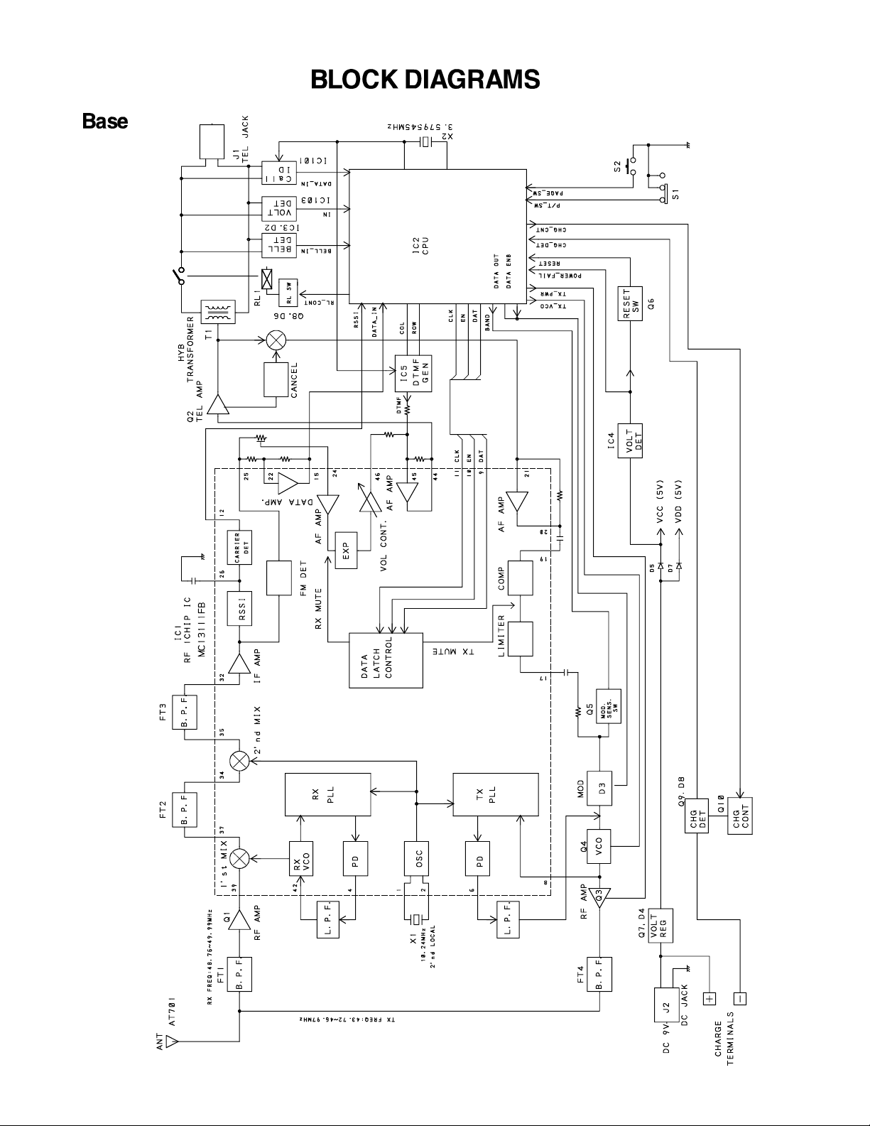
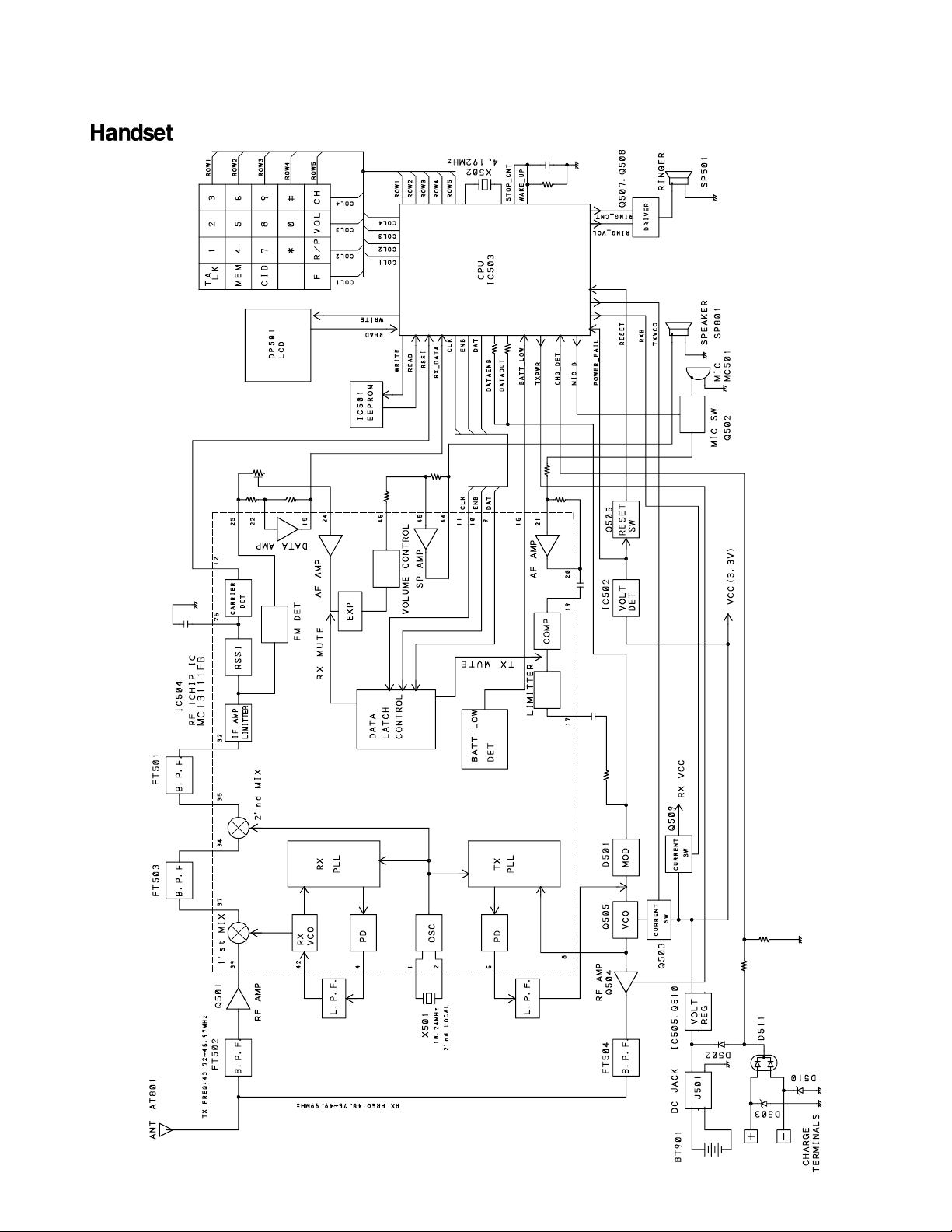
BLOCK DIAGRAMS..............................................................................................................................7
SCHEMATIC DIAGRAMS.....................................................................................................................9
TROUBLESHOOTING HINTS ........................................................................................................... 13
IC AND TRANSISTOR VOLTAGE CHART ....................................................................................... 19
SEMICONDUCTOR LEAD IDENTIFICATION...................................................................................23
ELECTRICAL PARTS LOCATION ..................................................................................................... 27
WIRING DIAGRAM.............................................................................................................................29
EXPLODED VIEW AND MECHANICAL PARTS LIST ...................................................................... 30
PARTS LIST ........................................................................................................................................34
ASSEMBLY PARTS LIST ...................................................................................................................48
SPECIFICATIONS .............................................................................................................................. 49
APPENDIX .......................................................................................................................................... 52
SAFETY PRECAUTIONS
Before returning any models to the customer, a safety check of the entire instrument should be made.
The service technician must be sure that no protective device built into the instrument by the manufacturer
has become defective or inadvertently degraded during servicing.
1. WARNING:
Alterations of the design or circuitry of these models should not be made.
Any design changes or additions such as, but not limited to, circuit modifications, auxiliary speaker
jacks, switches, grounding, active or passive circuitry, etc. may alter the safety characteristics of these
models and potentially create a hazardous situation for the user.
Any design alterations or additions will void the manufacturer’s warranty and will further relieve the
manufacturer of responsibility for personal injury or property damage resulting therefrom.
2. PRODUCT SAFETY NOTICE
Many electrical and mechanical parts in this chassis have special characteristics. These characteristics
often pass unnoticed and the protection afforded by them cannot necessarily be obtained by using
replacement components rated for higher voltage, wattage, etc. Replacement parts that have these
special safety characteristics are identified in this manual and its supplements; electrical components
having such features are identified by a in the schematic diagram and the parts list. Before replacing
any of these components, read the parts list in this manual carefully. The use of substitute replacement
parts that do not have the same safety characteristics as specified in the parts list may create shock, fire
or other hazards.
— 1 —
Page 3
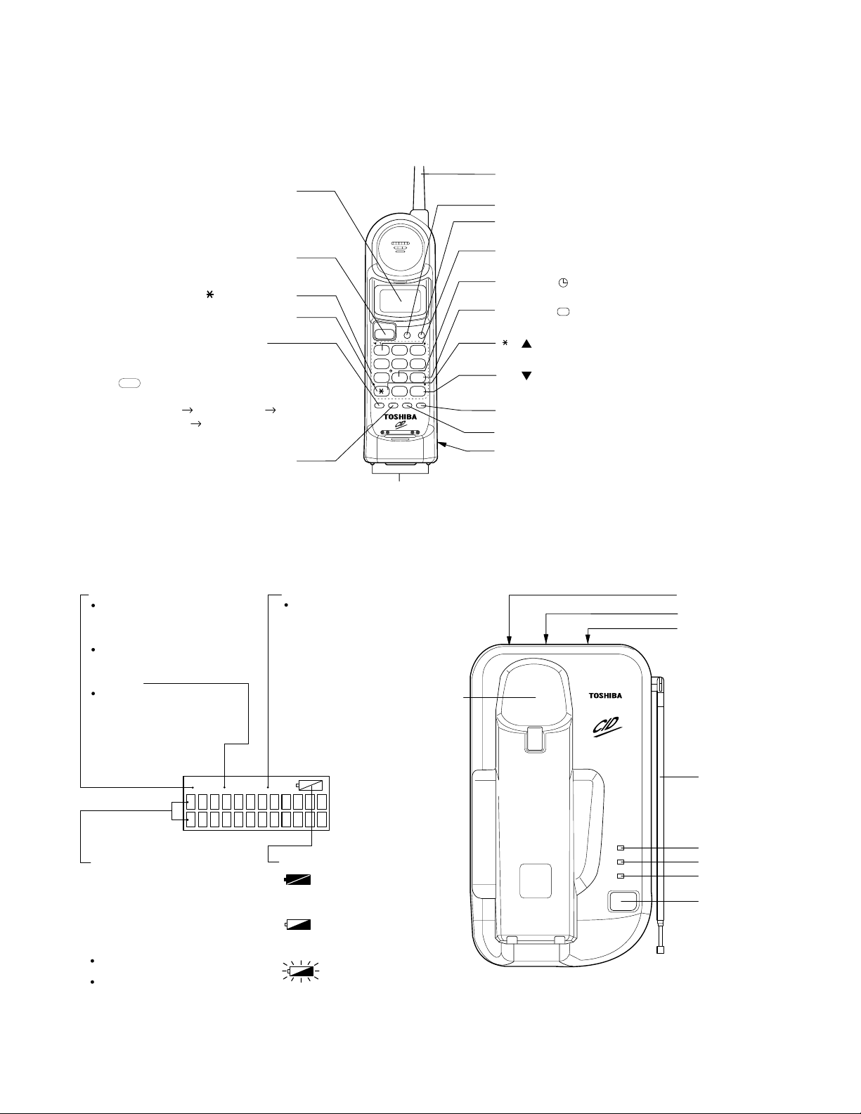
HANDSET CONTROLS
ging
Liquid Crystal Display (LCD)
TALK button
0-9, , # Dial buttons
TONE button
FLASH/FUNC (Function) button
Press to enter the Function Mode to
perform various settings. Each time
FUNC
the button is pressed, the
menu changes in the following order:
DIAL MEMORY AREA CODE
CIDCW ON\OFF AUTO TALK
ON\OFF.
CH (channel)/DELETE button
OPERATING CONTROLS
Helical antenna
MEM button
CID (Caller ID) button
Press to enter the caller ID mode.
Number 1 button
Used for long distance dialing.
Number 8 ( ) button (time button)
Used to display the date and time of the received calls.
TALK
MEM CID
ABC
DEF
JKL
GHI
MNO
"
#
PQ
WX
TUV
RS
Y Z
%
&
TONE
OPER
FLASH CH VOL/RING RDL
FUNC DELETE CANCELPAUSE
Number 9 ( ) button
Used to display the number of calls attempted by a caller
!
$
'
( ) button (up arrow button)
Used to scroll up the display screen.
( ) button (down arrow button)
Used to scroll down the display screen.
RDL(Redial)/PAUSE button
VOL/RING/CHANCEL button
Battery compartment
.
talk icon
Blinks
-while the handset is connecting
to the base unit.
-when a channel is being changed.
Displayed during a call in progress
on the handset.
call id icon
Displayed during the caller ID
review mode.
talk
Dot matrix display
Twelve digits by two lines dot
matrix LCD. Shows the time, caller
ID, memory location, instructions,
error messages, and other
information.
call id mem
Char
mem icon
Displayed
-while data is being stored in an
deleted from memory.
-while the Function Mode is in
use.
contacts
Battery icon
Displayed while the handset is being
charged.
BASE UNIT CONTROLSLCD
Cradle
ALL DIGITAL CALLER ID
CORDLESS TELEPHONE
25 CH SCANNING FT-7807
IN USE
CHARGE
POWER
PAGE
LINE modular jack
DC IN 9V jack
Tone/Pulse switch
Base antenna
IN USE LED
CHARGE LED
POWER LED
PAGE button
The back light of the LCD operates
in the following manner:
Turns on during an incoming call
when the ringer is OFF.
Turns on for 5 seconds and then
off
-when a button is pressed (except
in battery low status).
-when the phone rings and the
handset is lifted from its cradle on
the base unit to answer a call.
Displayed while the handset is being
charged during the battery low status.
Blinks when the battery low status
occurs during standby and phone
conversation.
— 2 —
Page 4
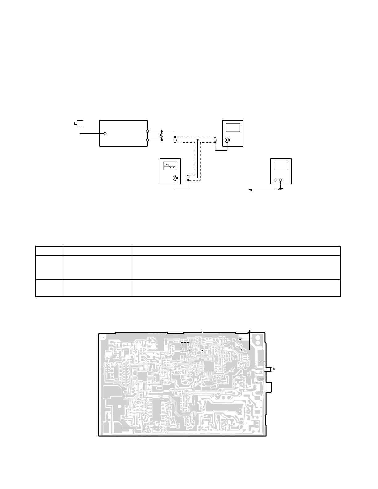
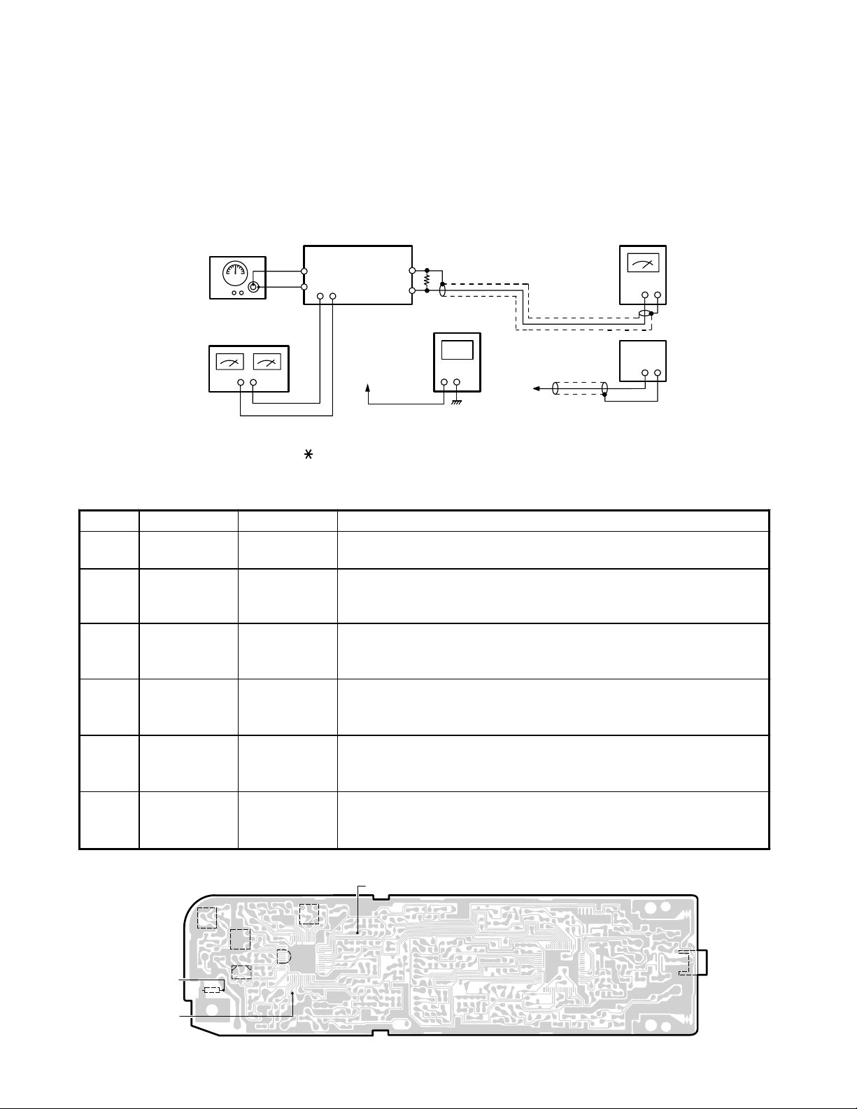
ALIGNMENT PROCEDURE
BASE UNIT / TRANSMITTER
Test Equipment Required and Connections
• Oscilloscope • Dummy Load, 50-ohm
• Frequency Counter • AC Power Supply: 120V, 60Hz (With AC Adapter)
• Digital Voltmeter
AC Adapter
(120V 60Hz)
Base Unit
J2
DC IN 9V
JACK
RF Test
Point
Dummy Load
(50-ohm)
−
+
Oscilloscope Digital Voltmeter
Frequency Counter
TX VCO
Test Point
Preset
a) Set T/P SW to Pulse Mode.
b) Turn on AC power while the Page key is being depressed.
c) Release the Page key about 2 seconds later, then the TX Mode is entered (CH21).
Alignment Procedure
Step Adjustment Remarks
Connect the oscilloscope across a 50-ohm load to RF test point.
1L10
2
Set the digital voltmeter at the test point of TX VCO.
Adjust L10 to indicate DC 2.8 ±0.05 V (VCO).
Connect the frequency counter across a 50-ohm dummy load to RF test
point. Make sure that the frequency is 46.770 MHz ±1500 Hz.
Alignment Point Location on Main (Base Unit) PCB
TX VCO Test Point
L10
— 3 —
RF Test Point
L1
S1
J2
P
T/P SW
T
DC IN 9V J a c k
Page 5
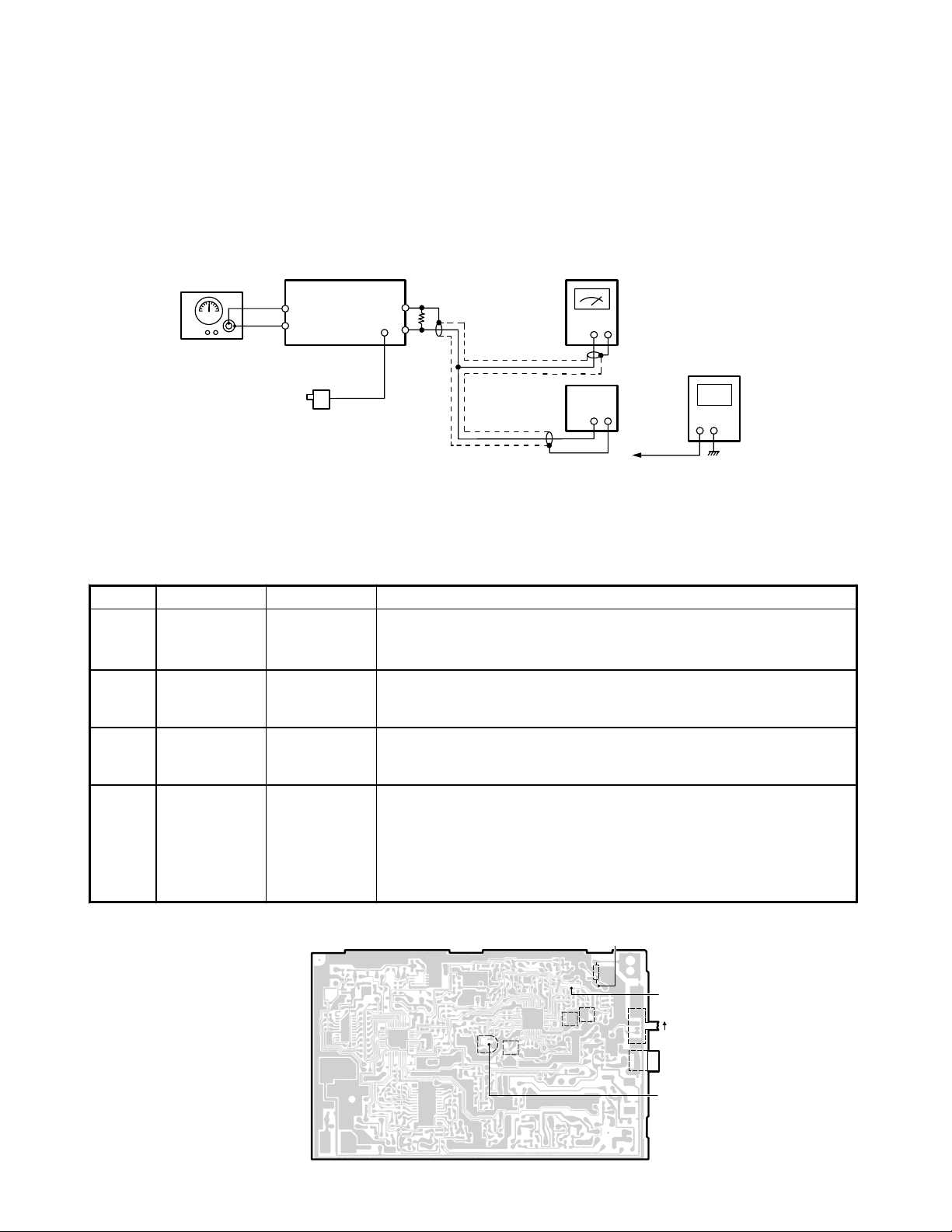
RECEIVER
k
Test Equipment Required and Connections
• SG: RF Signal Generator, 49.830 MHz, 49.160 MHz • Dummy Load, 600-ohm
• Digital Voltmeter • AF SSVM
• SINAD Meter
SG
+
MOD = 1KHz
DEV = ±3kHz
Base Unit AF SSVM
Dummy Load
RF Test
Point
TEL Jack
(600-ohm)
Digital Voltmeter
AC Adapter
(120V 60HZ)
SINAD
Meter
RX VCO
Test Point
Preset
a) Set T/P SW to Pulse Mode.
b) Turn on AC power while the Page key is being depressed.
c) Release the Page key about 2 seconds later, then the TX Mode is entered (CH21).
d) Press the Page key 4 times, then the RX Mode is entered (CH21).
Alignment Procedure
Step Preset to Adjustment Remarks
Connect the SG to the RF test point.
Connect the digital voltmeter to the test point of the RX VCO.
Adjust L7 to indicate DC 1.4 ±0.05 V.
Connect the digital voltmeter to the test point of Discriminator.
Adjust L3 to indicate DC 2.0 ±0.05V.
Adjust RT1 to make AF SSVM value −5 dBm ±0.5 dB.
Set T/P SW to TONE Mode. Press the Page key once, then CH
changes to CH 8.
Connect the AF SSVM to the TEL LINE across a 600-ohm dummy
load.
Keep the SINA D re ad in g at 12 d B b y a dj usti ng t h e S G ou tp ut . Adju st
L6 for maximum SINAD reading.
1
No modulation
2
3
1 kHz ±3 kHz
4
1 kHz ±3 kHz
SG: 1 mV
SG: 1 mV
1 kHz ±3kHz
deviation
SG: 1 mV
deviation
SG: 1 mV
deviation
L7
L3
RT1
L6
Alignment Point Location on Main (Base Unit) PCB
RT1
— 4 —
L3
L7
RF Test Point
L1
L6
S1
J2
RX VCO
Test Point
P
T/P SW
T
DC IN 9V Jac
Discriminator
Test Point
Page 6
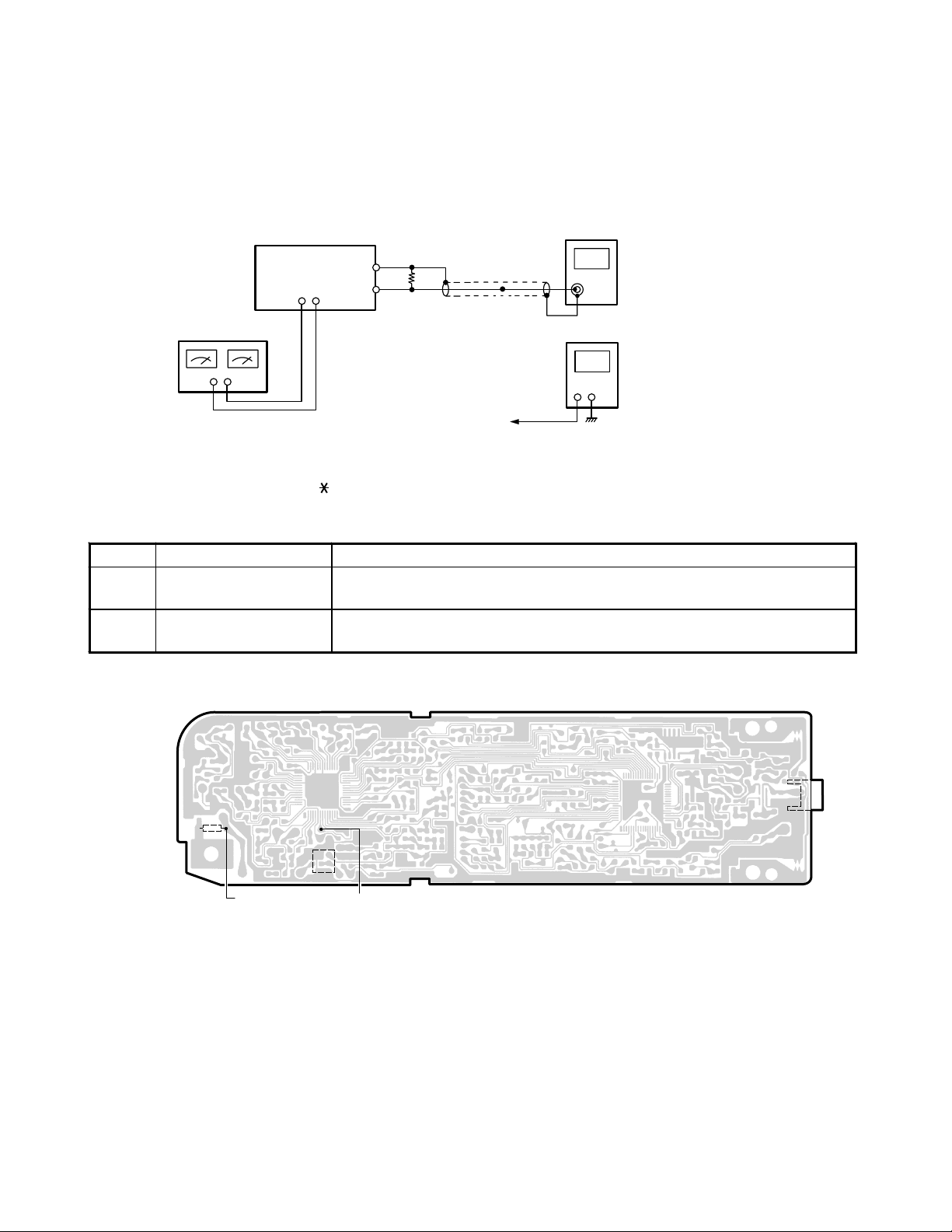
HANDSET / TRANSMITTER
Test Equipment Required and Connections
• DC Power Supply, 3.6V • Digital Voltmeter
Frequency Counter
Digital Voltmeter
TX VCO
Test Point
DC Power Supply
3.6V
Handset Unit
RF Test Point
Batt Termin a l
Dummy Load
(50-ohm)
+
Preset
Turn Power on while depressing “ ” and “#” keys. A beep will be heard. Then the TX Mode is entered (CH21).
Alignment Procedure
Step Adjustment Remarks
1L509
2
Set the digital voltmeter at the test point of TX VCO, then adjust L509 to
indicate DC 2.0 V ±0.05 V at CH21.
Connect the frequency counter across a 50-ohm dummy load to RF test
point. Make sure that the frequency is 49.830 MHz ±1500 Hz.
Alignment Point Location on Main (Handset Unit) PCB
L504
L509
RF
Test Point
TX VCO
Test Point
J501
Battery
Terminal
— 5 —
Page 7
RECEIVER
y
Test Equipment Required and Connections
• SG: RF Signal Generator, 46.770 MHz, 46.610 MHz • Dummy Load, 150-ohm
• VTVM • DC Power Supply: 3.6 V
• Digital Voltmeter • SINAD Meter
SG
MOD = 1KHz
DEV = ±3kHz
DC Power Supply
3.6V
Preset
a) Turn Power on while depressing “ ” and “#” keys. A beep will be heard. Then the TX Mode is entered (CH21).
b) Press “4” key, then the RX ADJ Mode is entered (CH21).
Alignment Procedure
Step Preset to Adjustment Remarks
1L505
SG: 1 mV
2
3
4
5
6
(CH21)
MOD OFF
SG: 1 mV
(CH21)
1 kHz ±3 kHz dev.
SG: 158 µV
(CH16)
1 kHz ±3 kHz dev.
SG: 3 µV
(CH16)
1 kHz ±3 kHz dev.
SG: 1 µV
(CH16)
1 kHz ±3 kHz dev.
L502
RT501
L510
L510 Adjust for maximum SINAD on the SINAD meter at CH16.
L510 Adjust for maximum SINAD on the SINAD meter at CH16.
Handset Unit VTVM
Dummy Load
+
RF Test
Point
Terminal
Batt Termin a l
RX VCO /
Discriminator
Test Point
SP
(150-ohm)
Digital Voltmeter
SP Terminal
across Dumm
Connect the digital voltmeter to the test point (RX VCO).
Adjust for 1.4 V DC at CH21.
Connect the digital voltmeter to th e test point (Discriminator).
Adjust for 1.1 V DC at CH21.
Connect the VTVM to the speaker terminal.
Adjust for 115 mV on the VTVM (SP. OUT) at CH21.
Press the “CH” twice to change the channel to CH16.
Adjust for maximum SINAD on the SINAD METER at CH16.
SINAD
Meter
Load
Alignment Point Location on Main (Handset Unit) PCB
Discriminator
Test Point
Terminal
RF
Test Point
RX VCO
Test Point
SP
L510
L504
L505
J502
L502
RT501
— 6 —
J501
Battery
Terminal
Page 8
— 7 —
Page 9
— 8 —
Page 10
TEST POINT
(Discriminator)
— 10 —
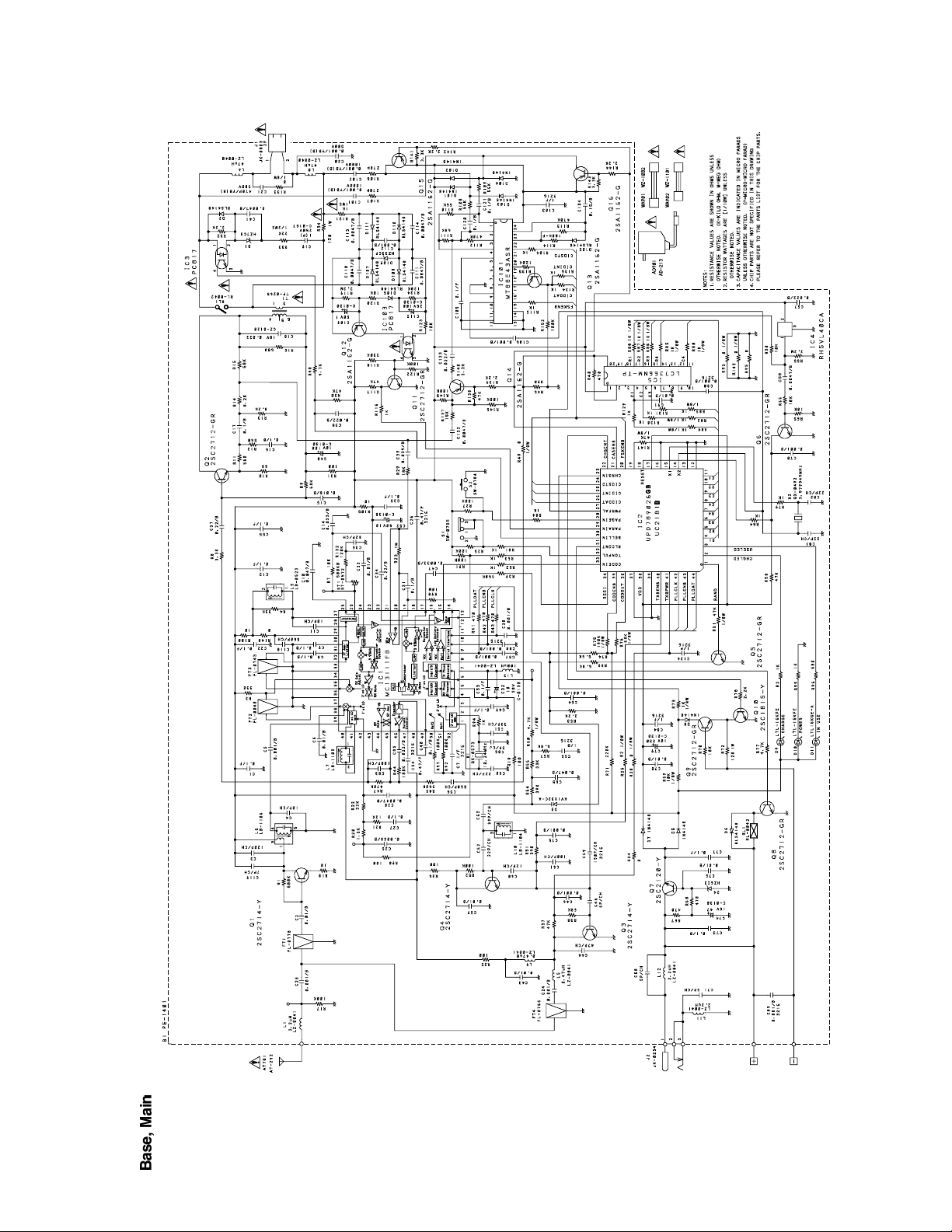
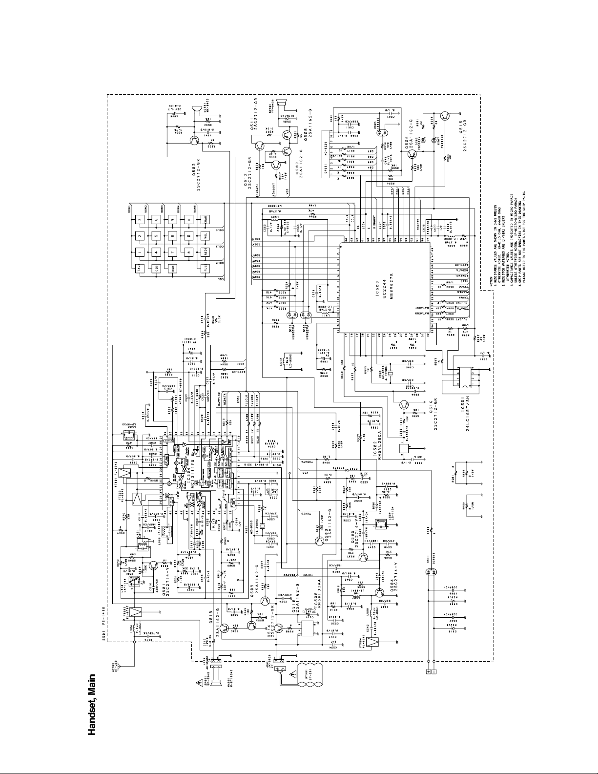
SCHEMATIC DIAGRAMS
(RF)
TEST POINT
TEST POINT
TEST POINT(TX VCO)
(RX VCO)
— 9 —
Page 11
TEST POINT
(Discriminator)
— 12 —
TEST POINT(TX VCO)
TEST POINT
(RX VCO)
— 11 —
TEST POINT
(RF)
Page 12
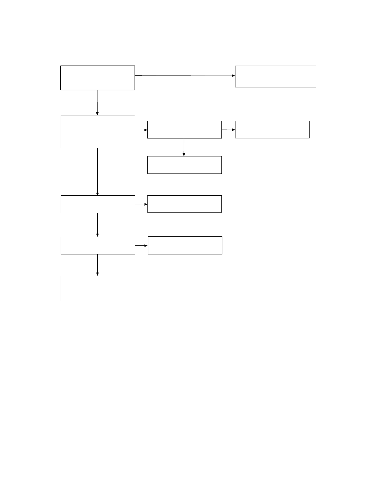
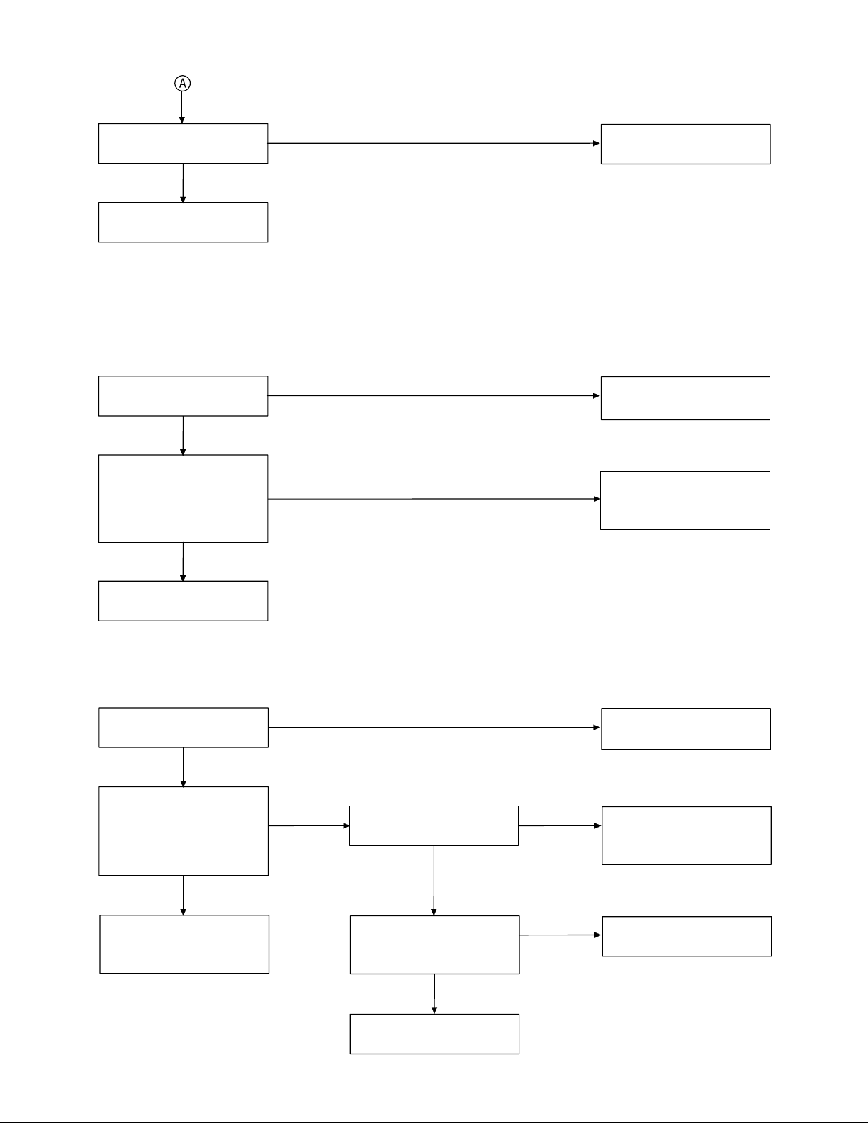
TROUBLESHOOTING HINTS
1. The bell does not ring.
When the PAGE SW of the
base is pressed, does the
ringer on the handset ring?
OK
When the TEL SG is joined
with the base to make bell
signal, is there pulse wave
on Pin 4 of IC3?
OK
Then, is there pulse wave
on Pin30 of IC2?
OK
By using voltage chart,
check IC2.
NG
NG
By using voltage chart,
check IC3.
Check TEL network
primary circuit.
NG
Check IC2, R30 and R48.
NG
IC2 is defective.
See 2. The bell does not ring
& page does not ring.
NG
IC3 is defective.
OK
OK
Check the surrounding
circuit where the
voltage is incorrect.
— 13 —
Page 13
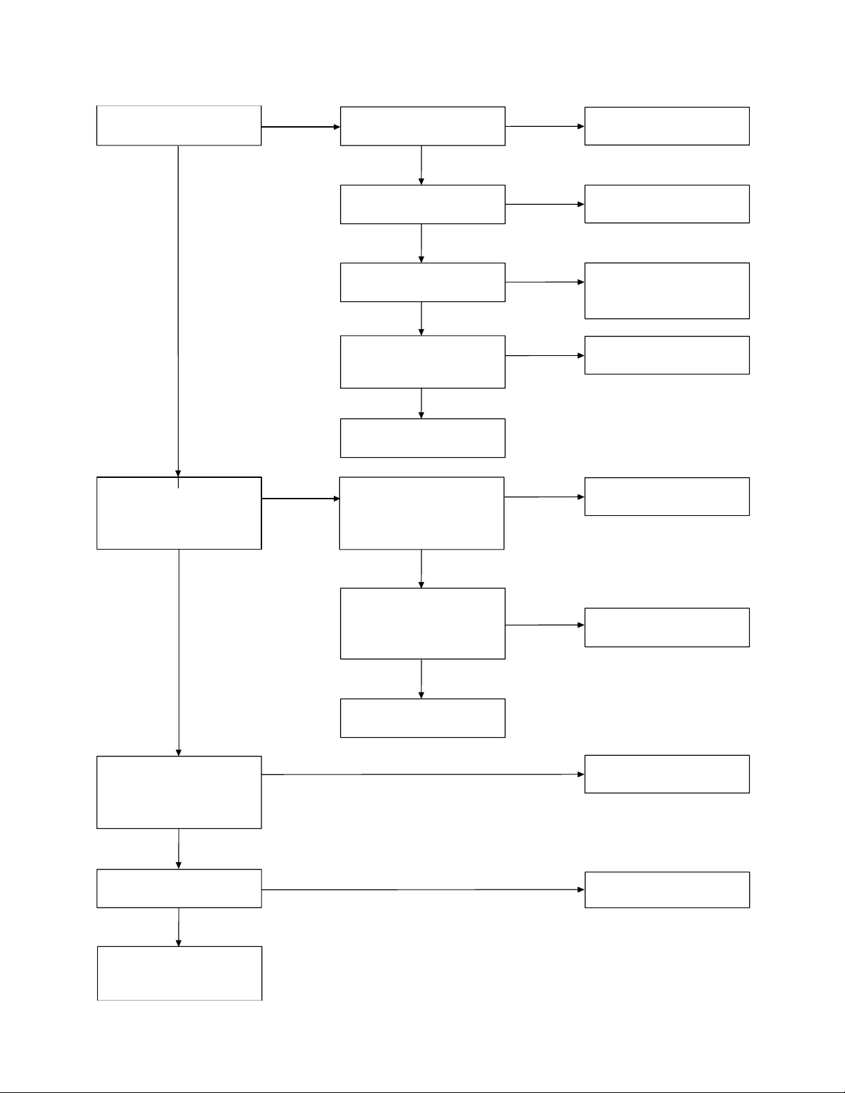
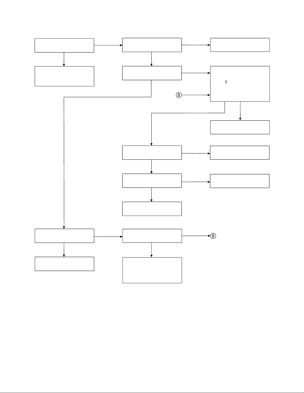
2. The bell does not ring & page does not ring.
Can the base and handset
be connected?
OK
Press handset DIAL key
while in TALK MODE. Can
key touch sound be heard
from the ringer?
NG
NG
Check the base TX power.
OK
Check the base TX data
deviation.
OK
Check the handset RX
sensitivity.
OK
Check RX data pulse
waveforming current
(Pin 15 of IC504).
OK
Check R515.
When the key of the
handset is pressed, can
the pulse output at pin 58
of IC503 be seen?
NG
NG
NG
NG
NG
By using voltage chart,
check the base TX circuit.
Check R53, R74, R71,
R75 and R76.
Check the handset RX RF
circuit (Q501) as well as
FT501 and FT503.
Check R505, C511 and
C539.
Check IC503.
OK
When the PAGE SW of the
base is pressed, does
Pin 28 of IC2 change from
high to low?
OK
By using voltage chart,
check IC2.
OK
Check the surrounding
circuit where the voltage is
incorrect.
NG
NG
OK
At the Q507 and Q512
collector, can the pulse
wave be seen?
OK
RINGER is defective.
NG
Check R556, R561, R569,
Q507 and Q512.
Check S2, R27 and R84.
IC2 is defective.
— 14 —
Page 14
3. The base and handset cannot connect.
Check whether the
handset and the base unit
are connected.
OK
Check the handset TX
POWER.
OK
NG
NG
Check the base TX power.
OK
Check the base TX data
deviation.
OK
Check the handset RX
sensitivity.
OK
Check the handset RX
data pulse wave forming
current (Pin 15 of IC503).
OK
Check R515.
NG
NG
NG
NG
By using voltage chart,
check the base TX circuit.
Check R53, R74, R71,
R75 and R76.
Check the handset RX RF
and mixer circuit (Q501) as
well as FT501 and FT503.
Check R505, C511 and
C539.
By using voltage chart,
check the handset TX
circuit.
Check the handset data
deviation.
OK
Check the base RX
sensitivity.
Then, can the sine wave
be seen at Pin 24 of IC1?
OK
NG
NG NG
NG
Check the handset MIC
sensitivity.
OK
Check the handset data
circuit (R540, R541, R584,
and R587).
Check the base RX TEL
OUT.
OK
Check the base RX RF and
mixer circuit (around Q1)
as well as FT3 and FT2.
NG
Check the handset TX AF
circuit (around Pins 17,
19 ~ 21 of IC504).
In the base, with the SG
standard modulation of
1kHz 3kHz deviation and
input signal of 1mV, can
the sine wave be seen at
Pin 25 of IC1?
OK
Check the base IF circuit
(around Pins 26~29 of IC1).
C heck circuit around P in 24
o f IC 1 .
NG
— 15 —
Page 15
Then, can the sine wave
be seen at the Q2 Collector.
OK
Check the surrounding
circuit of T1.
NG
4. Cannot make a phone call (pulse).
Check Q2 and surrounding
circuit of Q2.
Can the base and handset
be connected?
OK
While in TALK MODE,
press dial key of the
handset. Can pulse
feedback be heard from
the handset speaker?
OK
Check the base TEL-line
network primary circuit.
NG
NG
5. Cannot make a phone call (tone).
Can the base and handset
be connected?
OK
NG
See 3. The base and
handset cannot connect.
Check the base RELAY
control (around Pin23
of IC2.
See 3. The base and
handset cannot connect.
While in TALK MODE,
press dial key of the
handset. From the
speaker, does the TONE
ring up?
OK
Check the base TEL-line
circuit and RELAY control
circuit.
NG
Check the base modulation
sensitivity.
OK
At Pin 20 of IC5 of the
base, can the TONE
wave output be seen?
OK
Check R45, R46, R49 and
C56.
— 16 —
NG
NG
Check the base TX AF
circuit (around Pins 17,
19~21 of IC1).
Check IC5 by using
voltage chart.
Page 16
6. Voice cannot be transmitted to other party (outgoing call).
Check the handset MIC
sensitivity.
OK
Check the handset TX AF
circuit (around Pins 17,
19~21 of IC504).
NG
At the MIC of the handset,
does the bias voltage exist?
OK
Check the base RX
TEL-line out.
OK
Then, can the sine wave
be seen at Pin 24 of IC1?
OK
Then, can the sine wave be
seen at the Q2 collector?
NG
NG
NG
NG
Check R548, R534, R532
and C555.
In the base, with the SG
standard modulation of
1kHz 3kHz deviation and
input signal of 1mV, can
the sine wave be seen at
Pin 25 of IC1?
OK
Check the base IF circuit
(around Pins 26~29 of IC1).
Check circuit around Pin 24
of IC1.
Check Q2 and the
sorrounding circuit of Q2.
NG
Check the base RX
sensitivity.
OK OK
The handset MIC is
defective.
NG
OK
Check the sorrounding
circuit of T1.
Check the base RX
TEL-line out.
Check RX RF and mixer
circuit of the base (around
Q1) as well as FT3 and
FT2.
NG
— 17 —
Page 17

7. The voice of the caller cannot be heard (incoming call).
Check the handset RX SP
out.
OK
Check the handset RX
sensitivity.
OK NG
Check the handset RX RF
and mixer circuit (around
Q501) as well as FT501 and
FT503.
NG
In the handset, with the SG
standard modulation of
1kHz 3kHz deviation and
input signal of 1mV, can
the sine wave be seen at
Pin 25 of IC504?
OK
Then, can the sine wave
be seen at Pin 24 of IC504?
OK
Then, can the sine wave be
seen at Pin 46 of IC504
and C515?
OK
Then, can the sine wave of
the handset SP Limit be
seen?
OK
SP of handset is defective.
NG
NG
NG
NG
Check the handset IF
circuit (around Pins 26~29
of IC504).
Check circuit around Pin 24
of IC504.
Check around Pins 44~46,
52 of IC504.
The wire connecting the
handset SP is cut.
Check the base TX power.
OK
Check the base TX
modulation sensitivity.
OK
SP of handset is defective.
NG
NG
Check the base TX circuit
using voltage chart.
Check the base TX AF
circuit (around Pins 17,
19~21 of IC1).
— 18 —
Page 18

IC AND TRANSISTOR VOLTAGE CHART
Transistors Unit [V]
Ref.
Pin STBY TALK Note
No.
B 0.7 0.7
Q1 C 4.7 4.8
E 0.0 0.0
B 1.3 1.3
Q2 C 3.6 3.5
E 0.7 0.6
B 0.0 0.7
Q3 C 4.7 3.3~4.8
E 0.0 0.0
B 4.7 1.6~2.2
Q4 C 4.7 4.5
E 4.3 1.2~1.6
B 0.0~0.6 0.6
Q5 C 0.0 0.0
E 0.0 0.0
B 0.0 0.0
Q6 C 4.9 4.9
E 0.0 0.0
B 9.0 9.0
Q7 C 6.2 6.2
E 5.7 5.7
B 0.0 0.7
Q8 C 9.0 0.0
E 0.0 0.0
B 0.0 0.0
Q9 C 4.5 4.5
E 0.0 0.0
B 0.0 0.0
Q10 C 0.7 0.7
E 0.0 0.0
B 0.6 0.5
Q11 C 0.0 0.1
E 0.0 0.0
B 0.0 0.0
Q12 C 0.0 0.0
E 0.0 0.0
B 4.7 4.7
Q13 C 0.0 0.0
E 4.7 4.7
B 4.9 0.2
Q14 C 0.0 0.7
E 3.7 0.7
B 4.9 4.0
Q15 C 0.0 4.7
E 4.8 4.7
B 0.0 4.0
Q16 C 0.0 4.7
E 4.7 4.7
Ref.
Pin STBY TALK Note
No.
B 0.0~0.8 0.7
Q501 C 0.0~3.2 3.3
E 0.0 0.1
B 0.0 1.0
Q502 C 0.0 1.9
E 0.0 0.3
B 2.8~3.3 2.5
Q503 C 0.0 3.2
E 3.3 3.3
B 0.0 0.6~0.8
Q504 C 0.0 1.4~3.4
E 0.0 0.1
B 0.0 1.4~2.2
Q505 C 0.0 3.2
E 0.0 0.7~1.4
B 3.2 2.7
Q506 C 0.0~2.0 3.3
E 3.3 3.3
B 3.0 3.0
Q507 C 0.0 0.0
E 3.6 3.5
B 0.0 0.0
Q508 C 0.0 0.0
E 0.0 0.0
B 2.6 2.8
Q509 C 3.3 0.0~3.2
E 3.3 3.3
B 2.8 2.8~3.3
Q510 C 3.3 3.3
E 3.5 3.6
B 0.0 0.0
Q511 C 0.0 0.0
E 0.0 0.0
B 0.0 0.0
Q512 C 3.3 3.0
E 0.0 0.0
B 3.0 2.9
Q513 C 0.0 3.5
E 3.6 3.5
B 0.0~0.6 0.7
Q514 C 3.0 0.0
E 0.0 0.0
B 0.0 0.0
Q515 C 2.0 2.0
E 0.0 0.0
B 0.0 0.0
Q516 C 3.2 3.2
E 0.0 0.0
Unit [V]
—19—
Page 19

IC’S Unit [V]
Ref.
Pin STBY TALK Note
No.
1 0~4.2 0~4.2
2 0.4~4.0 0.4~4.0
3 1.5 1.5
4 0.0 0.0
5 4.5 4.5
6 4.5 1.5
7 0.0 0.0
8 4.5 4.2~4.7
9 0~4.9 0.0
10 0~4.9 0.0
11 0~4.9 0.0
12 0.0 0.0
13 4.7 0.0
14 0.0 0.0
15 0~4.7 0.0 DATA
16 0.0 0.0
17 1.5 1.5
18 4.7 4.6
19 1.5 1.5
20 1.5 1.5
21 1.5 1.5
22 4.0 4.0
23 4.7 4.7
24 1.1~1.7 1.4
25 0.1~0.3 1.8~2.3
IC1 26 0.4 1.5
27 4.6~4.9 4.6~4.9
28 3.7~4.7 3.7~4.0
29 4.8 4.7
30 4.1 4.1
31 4.1 4.1
32 4.1 4.0~4.2
33 0.0 0.0
34 4.7 4.7
35 3.2~3.7 3.3~3.6
36 0.0 0.0
37 3.5 3.3~3.6
38 4.7 4.7
39 4.7 4.7
40 0.3~0.5 0.3~0.5
41 0.0 0.3~0.5
42 0.0 0.1
43 0.0 0.0
44 1.5 1.5
45 1.5 1.5
46 1.5 1.5
47 4.7 4.7
48 1.5 1.5
49 0.0 1.5
50 0.0 0.0
51 0.0 0.0
52 1.5 1.5
Ref.
Pin STBY TALK Note
No.
1 0~4.9 4.9 DATA
2 4.9 4.9
3 4.9 0.1
4 0.0 0.0
5 0.0 0.0
6 0.0 0.0
7 0.0 0.0
8 0.0 0.0
9 0.0 0.0
10 0.0 0.0
11 0.0 0.0
12 0.0 0.0
13 0.0 0.0
14 2.0~3.6 2.0~3.6
15 2.0~3.1 2.0~3.2
16 0.0 0.0
17 4.9 4.9
18 4.9 0.0
19 0.0 0.0
20 0.0 0.0
21 4.7 0.1
IC2 22 4.9 4.8
23 4.7 4.7
24 0.0 0.0
25 0.0 0.0
26 0.0 0.0
27 4.9 4.7
28 4.9 4.7
29 0.0 0.1
30 0.0 4.7
31 0.0 4.9
32 4.7 4.7
33 0~4.7 4.7 DATA
34 4.7 0.1
35 0.0 0.0
36 0.1 0.1
37 0.0 0.0
38 4.9 4.9
39 0.0 0.0
40 4.3 0.1
41 0.0 4.9
42 0.0~4.9 0.0
43 0.0~4.9 0.0
44 0.0~4.9 0.0
1 0.0 0.0
2 0.0 0.0
IC3
3 0.0 0.0
4 5.0 5.0
1 4.7 4.7
IC4 2 4.7 4.7
3 0.0 0.0
Unit [V]
—20—
Page 20

IC’S Unit [V]
Ref.
Pin STBY TALK Note
No.
1 4.7 4.7
2 4.7 4.6
3 0.0 0.0
4 0.0 0.0
5 0.0 0.0
6 0.0 0.0
7 0.0 0.0
8 0.0 0.0
9 -0.8~0.9 -0.8~0.9
10 4.7 4.7
IC5
11 0.0 0.0
12 0.0 0.0
13 0.0 0.0
14 0.0 0.0
15 0.0 0.0
16 0.0 0.0
17 0.0 0.0
18 0.0 0.0
19 0.0 0.0
20 2.1 2.1
1 2.3 2.3
2 2.4 2.3
3 2.4 2.3
4 2.4 2.3
5 2.4 2.3
6 0.0 0.0
7 0.0 0.0
8 0.0 0.0
9 0.0 0.0
10 1.4~3.2 3.2~1.4
11 0.6~3.4 0.0
IC101 12 0.0 0.0
13 0.0 0.0
14 0.0 0.0
15 0.0 0.0
16 4.7 4.7
17 4.7 4.7
18 4.7 4.7
19 4.7 0.0
20 0.0 0.0
21 0.0 0.0
22 0.0 0.0
23 0.0 0.0
24 4.7 4.7
1 0.0 0.0
IC103
IC501
2 0.0 0.0
3 0.0 0.0
4 0.5 0.5
1 0.0 0.0
2 0.0 0.0
3 0.0 0.0
4 0.0 0.0
Ref.
Pin STBY TALK Note
No.
5 3.3 3.2
IC501
IC502 2 3.3 3.3
IC503 23 -0.1~3.0 -0.1~3.4
6 0.0 3.2
7 0.0 0.0
8 3.3 3.3
1 3.3 3.3
3 0.0 0.0
1 3.3 3.3
2 0.0 0.0
3 0.0 0.0
4 0.0 0.0
5 0.0 0.0
6 0.0 0.0
7 0.0 0.0
8 0.0 0.0
9 0.0 0.0
10 0.0 0.0
11 3.3 3.3
12 0.0 0.0
13 0.0 0.0
14 3.3 3.3
15 1.1~3.2 3.2
16 0.0 0.0
17 3.3 3.3
18 0.0 0.0
19 3.3 3.2
20 0.0 0.0
21 0.0 0.0
22 0.0~3.0 -0.1~3.0
24 0.0 0.0
25 0.0 0.0
26 0.0 0.0
27 0.0 0.0
28 0.0 0.0
29 0.0 0.0
30 0.0 0.0
31 0.0 0.0
32 0.0 3.3
33 3.3 3.3
34 1.1~3.3 3.3
35 0.0~3.2 0.0
36 0.0 0.0
37 0.0 0.1
38 0.0~3.2 0.0
39 0.0 1.3
40 0.0~3.2 0.0
41 2.8~3.3 0.0
42 0.0~3.3 0.0
43 0.0 0.0
44 0.0~3.2 0.1~3.2 DATA
45 0.0~3.2 3.2
46 0.0 0.0
Unit [V]
—21—
Page 21

Ref.
Pin STBY TALK Note
No.
47 0.0 0.0
48 0.0 0.0
49 0.0 0.0
50 0.0~2.7 0.0
51 0.0 0.0
52 0.0 0.0~3.3 DATA
53 0.0 0.0~3.3 DATA
54 0.0 0.0~3.2 DATA
IC503
IC504
55 0.0 0.0~3.2 DATA
56 3.3 3.3
57 3.3 0.0~3.2 DATA
58 0.0 0.0
59 0.0 0.0~3.2 DATA
60 3.3 0.0
61 0.0 0.0~3.2 DATA
62 3.3 3.3
63 3.3 3.3
64 3.3 3.3
1 0.0~2.6 0.3~2.5
2 0.0~2.6 0.4~2.7
3 0.0~2.8 1.5
4 0.0~3.2 1.2
5 0.0~3.3 3.2
6 0.1 1.3~2.7
7 0.0 0.0
8 0.0~3.3 3.0~3.6
9 0.0~3.3 0.1
10 0.0~3.2 0.1
11 0.0~3.2 0.1
12 0.0 0.0
13 0.0~3.2 0.0
14 0.0 0.0
15 0.0~3.2 0.0~3.2 DATA
16 0.0~33 3.2
17 0.0 1.5
18 0.0~3.3 3.2
19 0.0 1.5
20 0.0 1.5
21 0.0 1.5
22 0.1~1.8 2.5
23 0.0~3.3 3.3
24 0.0 1.5
25 -0.1~2.2 0.8~1.4
26 0.0~0.5 0.9
27 0.0~3.4 3.0~3.4
28 0.0~2.6 2.1~2.6
29 0.0~3.3 3.3
30 0.0~2.6 2.6
31 0.0~2.6 2.6
32 0.0~2.6 2.6
33 0.0 0.1
34 0.0~3.3 3.2
Unit [V]
Ref.
Pin STBY TALK Note
No.
35 0.0 2.0
36 0.0 0.1
37 0.0 1.8~2.0
38 0.0~3.3 3.2
39 0.0~3.3 3.3
40 0.0~0.7 0.3~0.6
41 0.0~0.7 0.3~0.6
42 0.0~3.0 1.3
IC504
IC505
43 0.0 0.0
44 0.0 1.5
45 0.0 1.5
46 0.0 1.5
47 0.0~3.3 3.2
48 0.0~0.3 1.5
49 0.0~0.3 1.5
50 0.0~1.6 1.6
51 0.0 0.0
52 0.0~1.5 1.5
1 0.0 0.0
2 3.6 3.6
3 3.3 3.3
4 2.9~3.4 2.9
5 0.0 0.0
Unit [V]
—22—
Page 22

Base Unit
SEMICONDUCTOR LEAD IDENTIFICATION
D1: HZ7C3
D4: HZ6C3
D5/D7/D8/D101/D102/
D103/D104: 1N4148
D109: HZ33CP
Cathode
D3: KV1832C
Cathode
Anode
Anode
D2/D6/D105/D106/D107/
D108/D110/D111: RLS4148
Cathode
D9/D10: LTL-16KPE-A
D11: LTL-16KGE-A
Cathode
Anode
Anode
Q1/Q3/Q4: 2SC2714-Y
Q2/Q5/Q6/Q8/Q9/Q11: 2SC2712-GR
Q12/Q13/Q14/Q15/Q16: 2SA1162-G
C
BE
B: Base
E: Emitter
C: Collector
Q7: 2SC2120-Y
Q10: 2SC1815-Y
E
C
B
B: Base
E: Emitter
C: Collector
— 23 —
Page 23

IC1
T
MC13111FB
IC2
µPD789026
LO2 In
LO2 Out
Vag
Rx PD
PLL Vref
Tx PD
GND PLL
TX VCO
Data
En
Clk
Clk Out
CD Out
IC3/IC103
PC817
1
1
2
3
4
5
6
7
8
9
10
11
12
13
VB
Ref2
Ref1
51
52
14
15
DA Out
BD2 Out
BD1 Out
Scr Out
E In
49
50
161718
C Cap
Tx Out
48
E Cap
47
19
C In
4
SA Out
E Out
SA In
44
45
46
20
21
22
Tx In
DA In
Amp Out
1
GND Audio
V Cap Ctrl
434241
23
24
Det Out
Vcc Audio
Rx Audio In
P13
LO1 In
LO1 Out
40
Mix1 In1
!'
Mix1 In2
38
37
Mix1 Out
36
GND RF
Mix2 Out
35
Mix2 In
34
SGND RF
33
Lim In
32
Lim C1
31
Lim C2
30
Vcc RF
29
Lim Out
28
Q Coil
27
25
26
RSSI
P12
P11
P10
P47/KR7
P46/KR6
P45/KR6
P44/KR4
P43/KR3
P42/KR2
P41/KR1
P40/KR0
P14
44
434241403938373635
1
2
3
4
5
6
7
8
9
10
11
1213141516171819202122
NC
IC(Vpp)
P15
X2
P16
X1
P17
Vss
Vss
VddNCP00
Vdd
RESET
P53
P52
P01
P51/T02
P02
34
33
32
31
30
29
28
27
26
25
24
23
P03
P04
P05
P06
P07
P20/ASCK/SCK0
P21TxD/SO0
P22/RxD/SI0
P30/INTP0
P31/INTP1
P32/INTP2/CPT2
P50/T10/T00
IC4 RH5VL40CA
V
DD
4
2
IC5
LC7366NM
1
V
DD
2
XMIT
3
C1
4
5
C2
6
C3
Vss
7
8
9
OSCI
10
OSCO
3
20
TONE OUT
19
CD
18
R1
17
16
R2
15
R3
R4
14
13
12
MUTE
11
C4
2
3
3
2
1
Vss
OU
IC101
MT88E43
IN+
IN
GS
VRef
CAP
TRIGin
TRIGRC
TRIGout
MODE
OSCin
OSCout
Vss
V
1
2
−
3
4
5
6
7
8
9
10
11
12
24
23
22
21
20
19
18
17
16
15
14
13
DD
St/GT
ESt
StD
INT
CD
DR
DATA
DCLK
FSKen
PWDN
IC
— 24 —
Page 24

Handset
D501: KV1832C
Cathode
D504: 1SS226
A
C / A
D502: 1N4148
D503/D510: HZ6C3
Cathode
Anode
Anode
D505/D507: PG3822K
C
Cathode
Anode
D506: RLS4148
Cathode
D511: DCB010
A
D508//D509: HSM88WA
A / A
Anode
CC
Q501/Q504/Q505: 2SC2714-Y
Q502/Q511/Q512/Q514/Q515/Q516: 2SC2712-GR
C
A
Q503/Q506/Q507/Q508/Q509/Q510/Q513: 2SA1162-G
C
BE
B: Base
E: Emitter
C: Collector
— 25 —
Page 25

T
IC501 24LC16BT/SN
A0
A1
A2
Vss
1
2
3
4
8
7
6
5
Vcc
WP
SCL
SDA
IC502 RH5VL28CA
3
2
1
V
Vss
DD
OU
IC503
MB89627R
P46/INT26
P47/INT27
P50/AN0
P51/AN1
P52/AN2
P53/AN3
P54/AN4
P55/AN5
P56/AN6
P57/AN7
AVcc
AVR
AVss
P60/INT10
P61/INT11
P62/INT12
P63/INT13
P64
RST
P45/IN25
P44/IN24
P43/IN23
P42/IN22
P41/IN21
P40/IN20
P36/WTO
VCC
X1
P37/PT0
Vss
P27
P26
P25
P24
64 63 62 61 60 59 58 57 56 55 54 53 52
1
2
3
4
5
6
7
8
9
10
11
12
13
14
15
16
17
18
19
20 21 22 23 24 25 26 27 28 29 30 31 32
X0
MOD0
MOD1
P35/PWC
P23
P34/PT02
P22/PPGI
P33/SI1
P21/PPGI
P32/SO1
P20/PWCI
51
P31/SCK1
50
P30/PPG03
49
VSS
48
P00
47
P01
46
P02
45
P03
44
P04
43
P05
42
P06
41
P07
40
P10
39
P11
38
P12
37
P13
36
P14
35
P15
34
P16
33
P17
IC504
MC13111FB
LO2 In
LO2 Out
Vag
Rx PD
PLL Vref
Tx PD
GND PLL
TX VCO
Data
En
Clk
Clk Out
CD Out
1
2
3
4
5
6
7
8
9
10
11
12
13
VB
Ref1
51
52
14
15
DA Out
BD1 Out
Ref2
Scr Out
E In
48
49
50
161718
C Cap
Tx Out
BD2 Out
E Cap
E Out
46
47
19
20
C In
Amp Out
SA In
45
21
Tx In
GND Audio
SA Out
44
434241
22
23
DA In
Vcc Audio
LO1 In
V Cap Ctrl
LO1 Out
40
Mix1 In1
39
Mix1 In2
38
37
Mix1 Out
36
GND RF
Mix2 Out
35
Mix2 In
34
SGND RF
33
Lim In
32
Lim C1
31
Lim C2
30
Vcc RF
29
Lim Out
28
Q Coil
27
24
25
26
RSSI
Det Out
Rx Audio In
IC505
RN5RF33AA
1
GND
2
V
DD
OUT
3
5
CE
EXT
4
— 26 —
Page 26

— 27 —
Page 27

— 28 —
Page 28

— 29 —
Page 29

EXPLODED VIEW AND MECHANICAL PARTS LIST
Base Unit
— 30 —
Page 30

Base Unit
QTY
LOC.
NO.
10 RC000941 SSCW802608N Screw, P Tight Bind HD + D2.6X8 NI 3
11 RC004028 SSCW802616N Screw, P Tight Bind HD + D2.6X16 NI 4
12 RC001752 SSCW283012N Screw, Tapping Bind+& SP Washer D3X12 NI 1
13 RC005524 GCAS356904Z Desk Top/Wall Mount Bracket ABS 1
14 RC005533 RUTC457141Z Wool Coated Paper, Wool Tack 1
15 RC005180 PLBZ456717Z Label, Indication 1
16 RC005531 PLBZ457408Z Label, Indication 1
PART NO. REF. NO. DESCRIPTION
1 RC005527 GNBZ356907Z Button, Push ABS 1
2 RC005523 GCAS356903Z Case, Bottom ABS 1
3 RC005522 GCAS156902Z Case, Top ABS 1
4 RC005665 HTML457208Z Charge Terminal (Comp) C5191(PBP) 2
5 RC008796 PLBS458442Z Label, ID 1
6 RC005532 RCLR419970Z Cushion Bumpon 2
7 RC002384 LFUT428079Z Foot Bumpon SJ-5916 1.6T 2
8 RC005526 GCAS456906Z Hook ABS 1
9 RC005525 GCAS456905Z LED Lens PMMA 1
— 31 —
Page 31

Handset
— 32 —
Page 32

Handset
QTY
LOC.
NO.
51 RC004280 HTML451205Z Antenna Contact C5191(PBP) 1
52 RC005561 RBLD456730Z Blind PVC 1
53 RC005551 GNBZ356911Z Button, Function ABS 1
54 RC005552 GNBZ456912Z Button, Push ABS 1
55 RC005547 GCAS156908Z Case, Front ABS 1
56 RC005548 GCAS356909Z Case, Rear ABS 1
57 RC005671 HTML457209Z Chage Terminal C2680(BSP) 1
58 RC005672 HTML457210Z Charge Terminal C2680(BSP) 1
59 RC005549 GCAS356910Z Case, Battery ABS 1
60 RC004286 RCUN451209Z Cushion Neoprene 1
61 RC005562 RCUN454106Z Cushion Neoprene 1
62 RC004687 RCUM441420A Cushion Batt Moltprene, Nitto #500 1
63 RC005556 LHDZ455784Z Dual Holder EPDM 1
64 RC005544 GHDZ456417Z Holder, Display PC 1
65 RC005545 HHDZ456419Z Holder, Display SPTE 1
66 RC005550 GHDZ356415Z Holder, Speaker ABS 1
67 RC003990 SSCW282616N Screw, Tapping Bind +&SP Washer D2.6X16 NI 1
68 RC005557 LNBZ356400Z Key Rubber SI 1
69 RC005555 KDPZ456988Z Plate, Didplay PMMA 1
70 RC005546 RETC456608Z Reflection Sheet 1
71 RC000941 SSCW802608N Screw, P Tight Bind HD + D2.6X8 NI 6
72 RC004285 PLBZ451727Z Label, Caution Paper 1
73 RC005560 PLBZ457411Z Label, Caution 1
74 RC008803 PLBS458443Z Label, ID 1
75 RC005559 PLBS457410Z Label, ID 1
PART NO. REF. NO. DESCRIPTION
— 33 —
Page 33

PARTS LIST
20+80
0.5
PRODUCT SAFETY NOTE: Products marked with a have special characteristics important to safety.
Before replacing any of these components, read carefully the product safety notice of this service manual.
Don't degrade the safety of the product through important servicing.
Symbol F G J K M N Z P Symbol C D
% ±1 ±2 ±5 ±10 ±20 ±30 −
0+100 pF ±0.25 ±
LOC.
NO.
CAPACITORS
The following codes indicate variation of capacitors against temperatures,:
YA = ±5%, YB = ±10%, YD = +20 −30%, YE = +20 −50% (−25 ~ +85 °C), ZF = +30 −80%, (−10 ~ +79 °C),
CH = 0 ±60 ppm/°C, TH = −470 ppm/°C, ±60 ppm/°C, B = ±10%, F = +30 −80%,
SL = +350 ppm/
C1 RC004741 BCUP811040Z CERAMIC 0.1UF 50V Z F
C2 RC004497 BCUB811035Z CERAMIC 0.01UF 50V K B
C3 RC004736 BCUA811214Z CERAMIC 120PF 50V J CH
C4 RC004477 BCUA811002Z CERAMIC 10PF 50V D CH
C5 RC004496 BCUB811025Z CERAMIC 0.001UF 50V K B
C6 RC004497 BCUB811035Z CERAMIC 0.01UF 50V K B
C7 RC004508 BCXC311050Z CERAMIC 1UF 16V Z F
C8 RC004494 BCUB511045Z CERAMIC 0.1UF 25V K B
C9 RC004494 BCUB511045Z CERAMIC 0.1UF 25V K B
C10 RC004502 BCUB814735Z CERAMIC 0.047UF 50V K B
C11 RC004477 BCUA811002Z CERAMIC 10PF 50V D CH
C12 RC004741 BCUP811040Z CERAMIC 0.1UF 50V Z F
C14 RC004739 BCUB813335Z CERAMIC 0.033UF 50V K B
C15 RC004498 BCUB811535Z CERAMIC 0.015UF 50V K B
C16 RC004494 BCUB511045Z CERAMIC 0.1UF 25V K B
C17 RC004494 BCUB511045Z CERAMIC 0.1UF 25V K B
C18 RC000777 BCZY0120001 SEMI-CONDUCTOR 0.022UF 18V CZ-120
C19 RC003189 BCQL521055Z MYLAR 1UF 250V K C-167
C20 RC000752 BCKB821025Z CERAMIC 0.001UF 500V K YB(B)
C21 RC004411 BCKB824715A CERAMIC 470PF 500V K B C-080
C22 RC004741 BCUP811040Z CERAMIC 0.1UF 50V Z F
C23 RC004496 BCUB811025Z CERAMIC 0.001UF 50V K B
C24 RC004496 BCUB811025Z CERAMIC 0.001UF 50V K B
C25 RC004573 BCUB816825Z CERAMIC 0.0068UF 50V K B
C26 RC004960 BCXC514740Z CERAMIC 0.47UF 25V Z F
C27 RC004494 BCUB511045Z CERAMIC 0.1UF 25V K B
C28 RC004562 BCUB814725Z CERAMIC 0.0047UF 50V K B
C30 RC004496 BCUB811025Z CERAMIC 0.001UF 50V K B
C31 RC004494 BCUB511045Z CERAMIC 0.1UF 25V K B
C32 RC004951 BCAP811006Z ELECTROLYTIC 10UF 50V M C-130
C33 RC004497 BCUB811035Z CERAMIC 0.01UF 50V K B
C34 RC004608 BCUB312245Z CERAMIC 0.22UF 16V K B
C35 RC004741 BCUP811040Z CERAMIC 0.1UF 50V Z F
PART NO.
°C ~ −1000 ppm/°C, UJ = −750 ppm/°C ±120 ppm/°C, CJ = 0 ± 120 ppm/°C, CK = 0 ± 250 ppm/°C
REF
NO.
DESCRIPTION
— 34 —
Page 34

LOC.
NO.
PART NO.
REF
NO.
DESCRIPTION
C36 RC004492 BCUA818204Z CERAMIC 82PF 50V J CH
C37 RC004608 BCUB312245Z CERAMIC 0.22UF 16V K B
C38 RC004500 BCUB812235Z CERAMIC 0.022UF 50V K B
C39 RC004561 BCUB813935Z CERAMIC 0.039UF 50V K B
C40 RC004945 BCAP111016Z ELECTROLYTIC 100UF 10V M C-130
C41 RC004562 RCUB814725Z CERAMIC 0.0047UF 50V K B
C43 RC004497 BCUB811035Z CERAMIC 0.01UF 50V K B
C44 RC004487 BCUA814704Z CERAMIC 47PF 50V J CH
C45 RC004490 BCUA816092Z CERAMIC 6PF 50V D CH
C46 RC004496 BCUB811025Z CERAMIC 0.001UF 50V K B
C47 RC004560 BCUB813325Z CERAMIC 0.0033UF 50V K B
C48 RC004494 BCUB511045Z CERAMIC 0.1UF 25V K B
C49 RC004741 BCUP811040Z CERAMIC 0.1UF 50V Z F
C50 RC004482 BCUA812204Z CERAMIC 22PF 50V J CH
C51 RC004485 BCUA813304Z CERAMIC 33PF 50V J CH
C52 RC004951 BCAP811006Z ELECTROLYTIC 10UF 50V M C-130
C53 RC004741 BCUP811040Z CERAMIC 0.1UF 50V Z F
C54 RC004960 BCXC514740Z CERAMIC 0.47UF 25V Z F
C55 RC004741 BCUP811040Z CERAMIC 0.1UF 50V Z F
C56 RC004737 BCUA815614Z CERAMIC 560PF 50V J CH
C57 RC004500 BCUB812235Z CERAMIC 0.022UF 50V K B
C58 RC004562 BCUB814725Z CERAMIC 0.0047UF 50V K B
C59 RC004497 BCUB811035Z CERAMIC 0.01UF 50V K B
C60 RC004479 BCUA811204Z CERAMIC 12PF 50V J CH
C61 RC004478 BCUA811014Z CERAMIC 100PF 50V J CH
C62 RC004482 BCUA812204Z CERAMIC 22PF 50V J CH
C63 RC005388 BCUA813904Z CERAMIC 39PF 50V J CH
C64 RC004496 BCUB811025Z CERAMIC 0.001UF 50V K B
C65 RC004502 BCUB814735Z CERAMIC 0.047UF 50V K B
C66 RC005514 BCXB311055Z CERAMIC 1UF 16V K B
C68 RC004489 BCUA815091Z CERAMIC 5PF 50V C CH
C69 RC005513 BCXA811514Z CERAMIC 150PF 50V J CH
C70 RC004496 BCUB811025Z CERAMIC 0.001UF 50V K B
C71 RC004489 BCUA815091Z CERAMIC 5PF 50V C CH
C73 RC004494 BCUB511045Z CERAMIC 0.1UF 25V K B
C74 RC00494 BCAP314706Z ELECTROLYTIC 47UF 16V M C-130
C75 RC004496 BCUB811025Z CERAMIC 0.001UF 50V K B
C76 RC004497 BCUB811035Z CERAMIC 0.01UF 50V K B
C77 RC004741 BCUP811040Z CERAMIC 0.1UF 50V Z F
C78 RC004497 BCUB811035Z CERAMIC 0.01UF 50V K B
C79 RC005160 BCAP113316Z ELECTROLYTIC 330UF 10V M C-130
C80 RC004659 BCXB811025Z CERAMIC 0.001UF 50V K B
C81 RC004482 BCUA812204Z CERAMIC 22PF 50V J CH
C82 RC004482 BCUA812204Z CERAMIC 22PF 50V J CH
C83 RC004478 BCUA811014Z CERAMIC 100PF 50V J CH
C84 RC004508 BCXC311050Z CERAMIC 1UF 16V Z F
— 35 —
Page 35

LOC.
NO.
PART NO.
REF
NO.
DESCRIPTION
C85 RC004500 BCUB812235Z CERAMIC 0.022UF 50V K B
C86 RC004740 BCUE813091Z CERAMIC 3PF 50V C CJ
C87 RC004496 BCUB811025Z CERAMIC 0.001UF 50V K B
C88 RC004659 BCXB811025Z CERAMIC 0.001UF 50V K B
C89 RC004659 BCXB811025Z CERAMIC 0.001UF 50V K B
C91 RC004497 BCUB811035Z CERAMIC 0.01UF 50V K B
C101 RC005512 BCKB131025Z CERAMIC 0.001UF 1000V K YB(B)
C102 RC005512 BCKB131025Z CERAMIC 0.001UF 1000V K YB(B)
C103 RC004508 BCXC311050Z CERAMIC 1UF 16V Z F
C104 RC004559 BCUB311545Z CERAMIC 0.15UF 16V K B
C105 RC004741 BCUP811040Z CERAMIC 0.1UF 50V Z F
C106 RC004496 BCUB811025Z CERAMIC 0.001UF 50V K B
C109 RC004952 BCAP811096Z ELECTROLYTIC 1UF 50V M C-130
C110 RC004562 BCUB814725Z CERAMIC 0.0047UF 50V K B
C111 RC004562 BCUB814725Z CERAMIC 0.0047UF 50V K B
C112 RC004496 BCUB811025Z CERAMIC 0.001UF 50V K B
C113 RC004562 BCUB814725Z CERAMIC 0.0047UF 50V K B
C114 RC004562 BCUB814725Z CERAMIC 0.0047UF 50V K B
C115 RC004948 BCAP511016Z ELECTROLYTIC 100UF 25V M C-130
C118 RC004737 BCUA815614Z CERAMIC 560PF 50V J CH
C119 RC005182 BCUA817092Z CERAMIC 7PF 50V D CH
C120 RC004494 BCUB511045Z CERAMIC 0.1UF 25V K B
C121 RC004494 BCUB511045Z CERAMIC 0.1UF 25V K B
C122 RC004562 BCUB814725Z CERAMIC 0.0047UF 50V K B
C123 RC004500 BCUB812235Z CERAMIC 0.022UF 50V K B
C124 RC004508 BCXC311050Z CERAMIC 1UF 16V Z F
C501 RC004497 BCUB811035Z CERAMIC 0.01UF 50V K B
C502 RC004477 BCUA811002Z CERAMIC 10PF 50V D CH
C503 RC004482 BCUA812204Z CERAMIC 22PF 50V J CH
C504 RC004484 BCUA812704Z CERAMIC 27PF 50V J CH
C505 RC004497 BCUB811035Z CERAMIC 0.01UF 50V K B
C506 RC004502C BCUB814735Z CERAMIC 0.047UF 50V K B
C507 RC004502 BCUB814735Z CERAMIC 0.047UF 50V K B
C508 RC004502 BCUB814735Z CERAMIC 0.047UF 50V K B
C509 RC004500 BCUB812235Z CERAMIC 0.022UF 50V K B
C510 RC004502 BCUB814735Z CERAMIC 0.047UF 50V K B
C511 RC004739 BCUB813335Z CERAMIC 0.033UF 50V K B
C512 RC004956 BCUA811814Z CERAMIC 180PF 50V J CH
C513 RC004659 BCXB811025Z CERAMIC 0.001UF 50V K B
C514 RC004185 BCSS951006Z TANTALUM CHIP 10UF 7V M A C-241
C515 RC001045 BCEQ311006Z ELECTROLYTIC 10UF 16V M C-125
C516 RC004747 BCUA813314Z CERAMIC 330PF 50V J CH
C517 RC004478 BCUA811014Z CERAMIC 100PF 50V J CH
C518 RC004500 BCUB812235Z CERAMIC 0.022UF 50V K B
C519 RC004496 BCUB811025Z CERAMIC 0.001UF 50V K B
C520 RC004502 BCUB814735Z CERAMIC 0.047UF 50V K B
— 36 —
Page 36

LOC.
NO.
PART NO.
REF
NO.
DESCRIPTION
C521 RC004185 BCSS951006Z TANTALUM CHIP 10UF 7V M A C-241
C522 RC004497 BCUB811035Z CERAMIC 0.01UF 50V K B
C523 RC004491 BCUA816804Z CERAMIC 68PF 50V J CH
C524 RC004488 BCUA814714Z CERAMIC 470PF 50V J CH
C525 RC004502 BCUB814735Z CERAMIC 0.047UF 50V K B
C526 RC004497 BCUB811035Z CERAMIC 0.01UF 50V K B
C527 RC004497 BCUB811035Z CERAMIC 0.01UF 50V K B
C528 RC004481 BCUA811514Z CERAMIC 150PF 50V J CH
C529 RC001045 BCEQ311006Z ELECTROLYTIC 10UF 16V M C-125
C530 RC004497 BCUB811035Z CERAMIC 0.01UF 50V K B
C531 RC004497 BCUB811035Z CERAMIC 0.01UF 50V K B
C532 RC004494 BCUB511045Z CERAMIC 0.1UF 25V K B
C533 RC004573 BCUB816825Z CERAMIC 0.0068UF 50V K B
C534 RC004562 BCUB814725Z CERAMIC 0.0047UF 50V K B
C536 RC004659 BCXB811025Z CERAMIC 0.001UF 50V K B
C537 RC004564 BCUP514740Z CERAMIC 0.47UF 25V Z F
C538 RC004564 BCUP514740Z CERAMIC 0.47UF 25V Z F
C539 RC004608 BCUB312245Z CERAMIC 0.22UF 16V K B
C540 RC005165 BCUB811235Z CERAMIC 0.012UF 50V K B
C541 RC005667 BCUB811835Z CERAMIC 0.018UF 50V K B
C542 RC004496 BCUB811025Z CERAMIC 0.001UF 50V K B
C543 RC004485 BCUA813304Z CERAMIC 33PF 50V J CH
C544 RC004497 BCUB811035Z CERAMIC 0.01UF 50V K B
C545 RC004496 BCUB811025Z CERAMIC 0.001UF 50V K B
C546 RC004558 BCUA811804Z CERAMIC 18PF 50V J CH
C547 RC004478 BCUA811014Z CERAMIC 100PF 50V J CH
C548 RC004487 BCUA814704Z CERAMIC 47PF 50V J CH
C549 RC004477 BCUA811002Z CERAMIC 10PF 50V D CH
C550 RC004558 BCUA811804Z CERAMIC 18PF 50V J CH
C551 RC004496 BCUB811025Z CERAMIC 0.001UF 50V K B
C552 RC004502 BCUB814735Z CERAMIC 0.047UF 50V K B
C553 RC005514 BCXB311055Z CERAMIC 1UF 16V K B
C554 RC005166 BCUP311050Z CERAMIC 1UF 16V Z F
C555 RC004657 BCEQ514796Z ELECTROLYTIC 4.7UF 25V M C-125
C556 RC004497 BCUB811035Z CERAMIC 0.01UF 50V K B
C557 RC004497 BCUB811035Z CERAMIC 0.01UF 50V K B
C558 RC004504 BCXB511045Z CERAMIC 0.1UF 25V K B
C560 RC004741 BCUP811040Z CERAMIC 0.1UF 50V Z F
C561 RC004747 BCUA813314Z CERAMIC 330PF 50V J CH
C562 RC004494 BCUB511045Z CERAMIC 0.1UF 25V K B
C563 RC004741 BCUP811040Z CERAMIC 0.1UF 50V Z F
C564 RC008797 BCDU903316Z ELECTROLYTIC 330UF 6.3V M C-308
C565 RC004741 BCUP811040Z CERAMIC 0.1UF 50V Z F
C566 RC004494 BCUB511045Z CERAMIC 0.1UF 25V K B
C567 RC005134 BCUA812714Z CERAMIC 270PF 50V J CH
C568 RC004497 BCUB811035Z CERAMIC 0.01UF 50V K B
— 37 —
Page 37

LOC.
NO.
PART NO.
REF
NO.
DESCRIPTION
C569 RC005166 BCUP311050Z CERAMIC 1UF 16V Z F
C570 RC004741 BCUP811040Z CERAMIC 0.1UF 50V Z F
C571 RC004490 BCUA816092Z CERAMIC 6PF 50V D CH
C572 RC004496 BCUB811025Z CERAMIC 0.001UF 50V K B
C573 RC004747 BCUA813314Z CERAMIC 330PF 50V J CH
C574 RC004659 BCXB811025Z CERAMIC 0.001UF 50V K B
C576 RC008841 BCUC817581Z CERAMIC 0.75PF 50V C CK
C577 RC005166 BCUP311050Z CERAMIC 1UF 16V Z F
C578 RC004497 BCUB811035Z CERAMIC 0.01UF 50V K B
C580 RC003247 BCPT954796Z TANTALUM CHIP 4.7UF 7V M A C-228
C581 RC004741 BCUP811040Z CERAMIC 0.1UF 50V Z F
C582 RC004504 BCXB511045Z CERAMIC 0.1UF 25V K B
C583 RC004562 BCUB814725Z CERAMIC 0.0047UF 50V K B
C584 RC004496 BCUB811025Z CERAMIC 0.001UF 50V K B
C585 RC004482 BCUA812204Z CERAMIC 22PF 50V J CH
C586 RC004482 BCUA812204Z CERAMIC 22PF 50V J CH
C587 RC004483 BCUA812214Z CERAMIC 220PF 50V J CH
C588 RC004483 BCUA812214Z CERAMIC 220PF 50V J CH
C589 RC004497 BCUB811035Z CERAMIC 0.01UF 50V K B
C590 RC004497 BCUB811035Z CERAMIC 0.01UF 50V K B
DIODES
D1 RC002470 BDAY0492033 ZENER HZ7C3 TD
D2 RC001826 BDAY0433001 DIODE RLS4148 TE11
D3 RC005088 BDAY0943001 DIODE KV1832C-A TR
D4 RC002471 BDAY0492045 ZENER HZ6C3 TD
D5 RC002236 BDAY0246003 DIODE 1N4148 T-77
D6 RC001826 BDAY0433001 DIODE RLS4148 TE11
D7 RC002236 BDAY0246003 DIODE 1N4148 T-77
D8 RC002236 BDAY0246003 DIODE 1N4148 T-77
D9 RC004189 BDAY0866001 LED LTL-16KPE-A
D10 RC004189 BDAY0866001 LED LTL-16KPE-A
D11 RC004190 BDAY0867001 LED LTL16KGE-A
D101 RC002236 BDAY0246003 DIODE 1N4148 T-77
D102 RC002236 BDAY0246003 DIODE 1N4148 T-77
D103 RC002236 BDAY0246003 DIODE 1N4148 T-77
D104 RC002236 BDAY0246003 DIODE 1N4148 T-77
D105 RC001826 BDAY0433001 DIODE RLS4148 TE11
D106 RC001826 BDAY0433001 DIODE RLS4148 TE11
D107 RC001826 BDAY0433001 DIODE RLS4148 TE11
D108 RC001826 BDAY0433001 DIODE RLS4148 TE11
D109 RC003194 BDAY0272010 ZENER HZ33CP
D110 RC001826 BDAY0433001 DIODE RLS4148 TE11
D111 RC001826 BDAY0433001 DIODE RLS4148 TE11
D501 RC005088 BDAY0943001 DIODE KV1832C-A TR
D502 RC002236 BDAY0246003 DIODE 1N4148 T-77
— 38 —
Page 38

LOC.
PD S TX
RPF ND
NO.
PART NO.
REF
NO.
DESCRIPTION
D503 RC002471 BDAY0492045 ZENER HZ6C3TD
D504 RC001635 BDAY0274001 DIODE 1SS226 TE85L
D505 RC005534 BDAY0931001 LED PG3822K
D506 RC001826 BDAY0433001 DIODE RLS4148 TE11
D507 RC005534 BDAY0931001 LED PG3822K
D508 RC002240 BDAY0485001 DIODE HSM88WA TL
D509 RC002240 BDAY0485001 DIODE HSM88WA TL
D510 RC002471 BDAY0492045 ZENER HZ6C3 TD
D511 RC002658 BDAY0423002 DIODE DCB010 TB
FILTERS
FT1 RC004640 BFLY0778001 BPF FL-778 B803D-1087RX
FT2 RC002479 BFLY0048001 CERAMIC FL-048 SFE10.7MS2-M
FT3 RC004638 BFLY0743001 CERAMIC FL-743 LTW33-455D
FT4 RC004639 BFLY0766001 LC FL-766 B803D-1077TX
FT501 RC004638 BFLY0743001 CERAMIC FL-743 LTW33-455D
FT502 RC004664 BFLY0767001 LC FL-767 SH829D-1079RX
FT503 RC002479 BFLY0048001 CERAMIC FL-048 SFE10.7MS2-M
FT504 RC004397 BFLY0742001 FILTER FL-742 H829D-1001TX
IC’s
IC1 RC004706 BDEY2916001 MC13111FB
IC2 RC008808 BDDY0722003 UC2181B
IC3 RC000802 BDEY0577001 PC817 or
RC000802 BDEY0577001 TLP521-1
IC4 RC005075 BDEY2938003 RH5VL40CA-T1 or
RC005075 BDEY2938003 S80740AL-A4-T1
IC5 RC005516 BDEY1058003 LC7366NM-TP-T2
IC101 RC008809 BDEY3544003 MT88E43ASR
IC103 RC000802 BDEY0577001 PC817 or
RC000802 BDEY0577001 TLP521-1
IC501 RC008799 BDEY3181003 24LC16BT/SN
IC502 RC005074 BDEY2937003 RH5VL28CA-T1 or
RC005074 BDEY2937003 S80728AL-AR-T1
IC503 RC008798 BDDY0785001 UC2244
IC504 RC004706 BDEY2916001 MC13111FB
IC505 RC008800 BDEY3643003 RN5RF33AA-TR
JACKS
J1 RC003586 BJKY0803002 TEL JK-803 A36-006-4910A 2P
J2 RC001094 BJKY0234001 JACK JK-234 DJ13-1
J501 RC003619 BJKY0628001 JACK JK-628 M60-02-30-134P-6
J502 RC002252 BJKY0600002 JACK JK-600 SB20-02WS 2P
COILS
L1 RC004249 BLZY0041229 INDUCTOR LZ-041 2.2UH K
L3 RC004666 BLBY0523001 COIL LB-523 L7BRE-1293Z
— 39 —
Page 39

LOC.
NO.
PART NO.
REF
NO.
DESCRIPTION
L4 RC004248 BLZY0040470 INDUCTOR LZ-040 47UH
L5 RC003693 BLZY0041478 INDUCTOR LZ-041 0.47UH K
L6 RC004643 BLBY1106001 COIL LB-1106 PD600XCAS-9475RS
L7 RC004642 BLBY1105001 COIL LB-1105 291XCAS-9471IB
L8 RC004248 BLZY0040470 INDUCTOR LZ-040 47UH
L9 RC003693 BLZY0041478 INDUCTOR LZ-041 0.47UH K
L10 RC004641 BLBY1104001 COIL LB-1104 291XCAS-9472IB
L11 RC004249 BLZY0041229 INDUCTOR LZ-041 2.2UH K
L12 RC004249 BLZY0041229 INDUCTOR LZ-041 2.2UH K
L13 RC001769 BLZY0041101 INDUCTOR LZ-041 100UH K
L501 RC004670 BLBY1110001 COIL LB-1110 PD600XCAS-9550X
L502 RC004666 BLBY0523001 COIL LB-523 L7BRE-1293Z
L503 RC005541 BLZY0080278 INDUCTOR LZ-080 0.27UH K TAPE
L504 RC004249 BLZY0041229 INDUCTOR LZ-041 2.2UH K
L505 RC004668 BLBY1108001 COIL LB-1108 291XCAS-9462IB
L506 RC005541 BLZY0080278 INDUCTOR LZ-080 0.27UH K TAPE
L507 RC004400 BLZY0041109 INDUCTOR LZ-041 1UH K
L508 RC004401 BLZY0041398 INDUCTOR LZ-041 0.39UH K
L509 RC005539 BLBY1134001 COIL LB-1134 291XCAS-9656IB
L510 RC004669 BLBY1109001 COIL LB-1109 P291XCAS-9459BY
L511 RC005541 BLZY0080278 INDUCTOR LZ-080 0.27UH K TAPE
L512 RC005540 BLZY0080100 INDUCTOR LZ-080 10UH K TAPE
T1 RC003234 BTFY0265001 TRANSFORMER TF-265 IT-24E-1B(R295403)
TRANSISTORS
Q1 RC002245 BDBC2714124 TRANSISTOR DB-718 2SC2714-Y TE85L
Q2 RC001637 BDBC2712303 TRANSISTOR DB-381 2SC2712-GR TE85L
Q3 RC002245 BDBC2714124 TRANSISTOR DB-718 2SC2714-Y TE85L
Q4 RC002245 BDBC2714124 TRANSISTOR DB-718 2SC2714-Y TE85L
Q5 RC001637 BDBC2712303 TRANSISTOR DB-381 2SC2712-GR TE85L
Q6 RC001637 BDBC2712303 TRANSISTOR DB-381 2SC2712-GR TE85L
Q7 RC000799 BDBC2120124 TRANSISTOR DB-300 2SC2120-Y
Q8 RC001637 BDBC2712303 TRANSISTOR DB-381 2SC2712-GR TE85L
Q9 RC001637 BDBC2712303 TRANSISTOR DB-381 2SC2712-GR TE85L
Q10 RC000796 BDBC1815124 TRANSISTOR DB-299 2SC1815-Y
Q11 RC001637 BDBC2712303 TRANSISTOR DB-381 2SC2712-GR TE85L
Q12 RC001081 BDBA1162107 TRANSISTOR DB-036 2SA1162-G(GR)TE85L
Q013 RC001081 BDBA1162107 TRANSISTOR DB-036 2SA1162-G(GR)TE85L
Q014 RC001081 BDBA1162107 TRANSISTOR DB-036 2SA1162-G(GR)TE85L
Q015 RC001081 BDBA1162107 TRANSISTOR DB-036 2SA1162-G(GR)TE85L
Q016 RC001081 BDBA1162107 TRANSISTOR DB-036 2SA1162-G(GR)TE85L
Q501 RC002245 BDBC2714124 TRANSISTOR DB-718 2SC2714-Y TE85L
Q502 RC001637 BDBC2712303 TRANSISTOR DB-381 2SC2712-GR TE85L
Q503 RC001081 BDBA1162107 TRANSISTOR DB-036 2SA1162-G(GR)TE85L
Q504 RC002245 BDBC2714124 TRANSISTOR DB-718 2SC2714-Y TE85L
Q505 RC002245 BDBC2714124 TRANSISTOR DB-718 2SC2714-Y TE85L
— 40 —
Page 40

LOC.
NO.
PART NO.
REF
NO.
DESCRIPTION
Q506 RC001081 BDBA1162107 TRANSISTOR DB-036 2SA1162-G(GR)TE85L
Q507 RC001081 BDBA1162107 TRANSISTOR DB-036 2SA1162-G(GR)TE85L
Q508 RC001081 BDBA1162107 TRANSISTOR DB-036 2SA1162-G(GR)TE85L
Q509 RC001081 BDBA1162107 TRANSISTOR DB-036 2SA1162-G(GR)TE85L
Q510 RC001081 BDBA1162107 TRANSISTOR DB-036 2SA1162-G(GR)TE85L
Q511 RC001637 BDBC2712303 TRANSISTOR DB-381 2SC2712-GR TE85L
Q512 RC001637 BDBC2712303 TRANSISTOR DB-381 2SC2712-GR TE85L
Q513 RC001081 BDBA1162107 TRANSISTOR DB-036 2SA1162-G(GR)TE85L
Q514 RC001637 BDBC2712303 TRANSISTOR DB-381 2SC2712-GR TE85L
Q515 RC001637 BDBC2712303 TRANSISTOR DB-381 2SC2712-GR TE85L
Q516 RC001637 BDBC2712303 TRANSISTOR DB-381 2SC2712-GR TE85L
RESISTORS
R1 RC004547 BRFX016844Z CARBON 680K 1/10W J BULK
R2 RC004512 BRFX011024Z CARBON 1K 1/10W J BULK
R3 RC004533 BRFX013314Z CARBON 330 1/10W J BULK
R4 RC004535 BRFX013334Z CARBON 33K 1/10W J BULK
R7 RC004513 BRFX011034Z CARBON 10K 1/10W J BULK
R8 RC004534 BRFX013324Z CARBON 3.3K 1/10W J BULK
R9 RC004546 BRFX016834Z CARBON 68K 1/10W J BULK
R10 RC004746 BRFX016804Z CARBON 68 1/10W J BULK
R11 RC004745 BRFX015614Z CARBON 560 1/10W J BULK
R12 RC004745 BRFX015614Z CARBON 560 1/10W J BULK
R13 RC004548 BRFX018224Z CARBON 8.2K 1/10W J BULK
R14 RC004548 BRFX018224Z CARBON 8.2K 1/10W J BULK
R15 RC004546 BRFX016834Z CARBON 68K 1/10W J BULK
R16 RC004544 BRFX016814Z CARBON 680 1/10W J BULK
R17 RC004514 BRFX011044Z CARBON 100K 1/10W J BULK
R18 RC004510 BRFX011004Z CARBON 10 1/10W J BULK
R19 RC004511 BRFX011014Z CARBON 100 1/10W J BULK
R20 RC004742 BRFX011524Z CARBON 1.5K 1/10W J BULK
R21 RC004516 BRFX011234Z CARBON 12K 1/10W J BULK
R22 RC004526 BRFX012234Z CARBON 22K 1/10W J BULK
R23 RC004515 BRFX011054Z CARBON 1M 1/10W J BULK
R24 RC004509 BRFX010004Z CARBON 0 1/10W J BULK
R25 RC004514 BRFX011044Z CARBON 100K 1/10W J BULK
R26 RC005664 BRFX188204Z CARBON 82 1/8W J BULK
R27 RC004514 BRFX011044Z CARBON 100K 1/10W J BULK
R28 RC004550 BRFX180004Z CARBON 0 1/8W J BULK
R29 RC004522 BRFX011834Z CARBON 18K 1/10W J BULK
R30 RC004539 BRFX014734Z CARBON 47K 1/10W J BULK
R31 RC004511 BRFX011014Z CARBON 100 1/10W J BULK
R32 RC004525 BRFX012224Z CARBON 2.2K 1/10W J BULK
R33 RC003231 BRSJ222234Z METAL OXIDE 22K 1/2WS J
R34 RC002350 BRSN101514Z METAL OXIDE(FORMED) 150 1W J (P=12.5)
R35 RC004511 BRFX011014Z CARBON 100 1/10W J BULK
— 41 —
Page 41

LOC.
NO.
PART NO.
REF
NO.
DESCRIPTION
R36 RC004511 BRFX011014Z CARBON 100 1/10W J BULK
R37 RC004539 BRFX014734Z CARBON 47K 1/10W J BULK
R38 RC004546 BRFX016834Z CARBON 68K 1/10W J BULK
R39 RC004543 BRFX015644Z CARBON 560K 1/10W J BULK
R40 RC004537 BRFX014714Z CARBON 470 1/10W J BULK
R41 RC004537 BRFX014714Z CARBON 470 1/10W J BULK
R42 RC004537 BRFX014714Z CARBON 470 1/10W J BULK
R43 RC004537 BRFX014714Z CARBON 470 1/10W J BULK
R44 RC004523 BRFX011844Z CARBON 180K 1/10W J BULK
R45 RC004543 BRFX015644Z CARBON 560K 1/10W J BULK
R46 RC004743 BRFX013914Z CARBON 390 1/10W J BULK
R47 RC004540 BRFX014744Z CARBON 470K 1/10W J BULK
R48 RC004538 BRFX014724Z CARBON 4.7K 1/10W J BULK
R49 RC004550 BRFX180004Z CARBON 0 1/8W J BULK
R50 RC004513 BRFX011034Z CARBON 10K 1/10W J BULK
R51 RC004743 BRFX013914Z CARBON 390 1/10W J BULK
R52 RC004514 BRFX011044Z CARBON 100K 1/10W J BULK
R53 RC004525 BRFX012224Z CARBON 2.2K 1/10W J BULK
R54 RC004572 BRFX013934Z CARBON 39K 1/10W J BULK
R55 RC004528 BRFX012254Z CARBON 2.2M 1/10W J BULK
R56 RC004535 BRFX013334Z CARBON 33K 1/10W J BULK
R57 RC004545 BRFX016824Z CARBON 6.8K 1/10W J BULK
R58 RC004539 BRFX014734Z CARBON 47K 1/10W J BULK
R59 RC004545 BRFX016824Z CARBON 6.8K 1/10W J BULK
R60 RC004965 BRFX184724Z CARBON 4.7K 1/8W J BULK
R61 RC004756 BRFX184734Z CARBON 47K 1/8W J BULK
R62 RC004512 BRFX011024Z CARBON 1K 1/10W J BULK
R63 RC004512 BRFX011024Z CARBON 1K 1/10W J BULK
R64 RC004512 BRFX011024Z CARBON 1K 1/10W J BULK
R65 RC004513 BRFX011034Z CARBON 10K 1/10W J BULK
R66 RC004513 BRFX011034Z CARBON 10K 1/10W J BULK
R67 RC004537 BRFX014714Z CARBON 470 1/10W J BULK
R68 RC004537 BRFX014714Z CARBON 470 1/10W J BULK
R69 RC004566 BRFX181034Z CARBON 10K 1/8W J BULK
R70 RC004513 BRFX011034Z CARBON 10K 1/10W J BULK
R71 RC004527 BRFX012244Z CARBON 220K 1/10W J BULK
R72 RC002830 BRSJ101214Z METAL OXIDE 120 1W J
R73 RC004551 BRFX181024Z CARBON 1K 1/8W J BULK
R74 RC004541 BRFX015624Z CARBON 5.6K 1/10W J BULK
R75 RC004567 BRFX181844Z CARBON 180K 1/8W J BULK
R76 RC005663 BRFX186834Z CARBON 68K 1/8W J BULK
R77 RC004538 BRFX014724Z CARBON 4.7K 1/10W J BULK
R78 RC004525 BRFX012224Z CARBON 2.2K 1/10W J BULK
R79 RC004512 BRFX011024Z CARBON 1K 1/10W J BULK
R80 RC004551 BRFX181024Z CARBON 1K 1/8W J BULK
R81 RC004512 BRFX011024Z CARBON 1K 1/10W J BULK
— 42 —
Page 42

LOC.
NO.
PART NO.
REF
NO.
DESCRIPTION
R82 RC004551 BRFX181024Z CARBON 1K 1/8W J BULK
R83 RC004551 BRFX181024Z CARBON 1K 1/8W J BULK
R84 RC004512 BRFX011024Z CARBON 1K 1/10W J BULK
R85 RC004551 BRFX181024Z CARBON 1K 1/8W J BULK
R86 RC004551 BRFX181024Z CARBON 1K 1/8W J BULK
R87 RC004551 BRFX181024Z CARBON 1K 1/8W J BULK
R88 RC004551 BRFX181024Z CARBON 1K 1/8W J BULK
R89 RC004551 BRFX181024Z CARBON 1K 1/8W J BULK
R90 RC004511 BRFX011014Z CARBON 100 1/10W J BULK
R91 RC004514 BRFX011044Z CARBON 100K 1/10W J BULK
R92 RC004514 BRFX011044Z CARBON 100K 1/10W J BULK
R93 RC004550 BRFX180004Z CARBON 0 1/8W J BULK
R94 RC004512 BRFX011024Z CARBON 1K 1/10W J BULK
R95 RC004509 BRFX010004Z CARBON 0 1/10W J BULK
R96 RC004544 BRFX016814Z CARBON 680 1/10W J BULK
R97 RC004514 BRFX011044Z CARBON 100K 1/10W J BULK
R98 RC004645 BRFX011064Z CARBON 10M 1/10W J BULK
R99 RC004512 BRFX011024Z CARBON 1K 1/10W J BULK
R100 RC004510 BRFX011004Z CARBON 10 1/10W J BULK
R104 RC004512 BRFX011024Z CARBON 1K 1/10W J BULK
R105 RC004510 BRFX011004Z CARBON 10 1/10W J BULK
R106 RC004532 BRFX012744Z CARBON 270K 1/10W J BULK
R107 RC004532 BRFX012744Z CARBON 270K 1/10W J BULK
R108 RC004542 BRFX015634Z CARBON 56K 1/10W J BULK
R109 RC004542 BRFX015634Z CARBON 56K 1/10W J BULK
R110 RC004542 BRFX015634Z CARBON 56K 1/10W J BULK
R111 RC004546 BRFX016834Z CARBON 68K 1/10W J BULK
R112 RC004540 BRFX014744Z CARBON 470K 1/10W J BULK
R113 RC004540 BRFX014744Z CARBON 470K 1/10W J BULK
R114 RC005520 BRFX011043Z CARBON 100K 1/10W F BULK
R115 RC004512 BRFX011024Z CARBON 1K 1/10W J BULK
R116 RC004512 BRFX011024Z CARBON 1K 1/10W J BULK
R117 RC004539 BRFX014734Z CARBON 47K 1/10W J BULK
R118 RC004536 BRFX013344Z CARBON 330K 1/10W J BULK
R119 RC004528 BRFX012254Z CARBON 2.2M 1/10W J BULK
R120 RC004513 BRFX011034Z CARBON 10K 1/10W J BULK
R121 RC004183 BRSJ001024Z METAL OXIDE 1K 1WS J
R122 RC004514 BRFX011044Z CARBON 100K 1/10W J BULK
R123 RC004513 BRFX011034Z CARBON 10K 1/10W J BULK
R124 RC004517 BRFX011244Z CARBON 120K 1/10W J BULK
R129 RC004512 BRFX011024Z CARBON 1K 1/10W J BULK
R130 RC004512 BRFX011024Z CARBON 1K 1/10W J BULK
R131 RC004512 BRFX011024Z CARBON 1K 1/10W J BULK
R132 RC004517 BRFX011244Z CARBON 120K 1/10W J BULK
R133 RC004550 BRFX180004Z CARBON 0 1/8W J BULK
R134 RC004512 BRFX011024Z CARBON 1K 1/10W J BULK
— 43 —
Page 43

LOC.
NO.
PART NO.
REF
NO.
DESCRIPTION
R135 RC004517 BRFX011244Z CARBON 120K 1/10W J BULK
R136 RC004512 BRFX011024Z CARBON 1K 1/10W J BULK
R137 RC004518 BRFX011534Z CARBON 15K 1/10W J BULK
R138 RC004539 BRFX014734Z CARBON 47K 1/10W J BULK
R139 RC004525 BRFX012224Z CARBON 2.2K 1/10W J BULK
R140 RC004534 BRFX013324Z CARBON 3.3K 1/10W J BULK
R141 RC004534 BRFX013324Z CARBON 3.3K 1/10W J BULK
R142 RC004525 BRFX012224Z CARBON 2.2K 1/10W J BULK
R143 RC004534 BRFX013324Z CARBON 3.3K 1/10W J BULK
R144 RC004525 BRFX012224Z CARBON 2.2K 1/10W J BULK
R145 RC004514 BRFX011044Z CARBON 100K 1/10W J BULK
R146 RC004514 BRFX011044Z CARBON 100K 1/10W J BULK
R147 RC004756 BRFX184734Z CARBON 47K 1/8W J BULK
R148 RC004509 BRFX010004Z CARBON 0 1/10W J BULK
R149 RC004550 BRFX180004Z CARBON 0 1/8W J BULK
R152 RC004514 BRFX011044Z CARBON 100K 1/10W J BULK
R501 RC004752 BRFX181014Z CARBON 100 1/8W J BULK
R502 RC004513 BRFX011034Z CARBON 10K 1/10W J BULK
R503 RC004539 BRFX014734Z CARBON 47K 1/10W J BULK
R504 RC004512 BRFX011024Z CARBON 1K 1/10W J BULK
R505 RC004513 BRFX011034Z CARBON 10K 1/10W J BULK
R506 RC004512 BRFX011024Z CARBON 1K 1/10W J BULK
R507 RC004512 BRFX011024Z CARBON 1K 1/10W J BULK
R508 RC004767 BRFX012233Z CARBON 22K 1/10W F BULK
R509 RC004517 BRFX011244Z CARBON 120K 1/10W J BULK
R510 RC004767 BRFX012233Z CARBON 22K 1/10W F BULK
R511 RC004512 BRFX011024Z CARBON 1K 1/10W J BULK
R512 RC004538 BRFX014724Z CARBON 4.7K 1/10W J BULK
R513 RC004551 BRFX181024Z CARBON 1K 1/8W J BULK
R514 RC004543 BRFX015644Z CARBON 560K 1/10W J BULK
R515 RC004513 BRFX011034Z CARBON 10K 1/10W J BULK
R516 RC004519 BRFX011544Z CARBON 150K 1/10W J BULK
R517 RC004551 BRFX181024Z CARBON 1K 1/8W J BULK
R518 RC004511 BRFX011014Z CARBON 100 1/10W J BULK
R519 RC004526 BRFX012234Z CARBON 22K 1/10W J BULK
R520 RC004510 BRFX011004Z CARBON 10 1/10W J BULK
R521 RC004566 BRFX181034Z CARBON 10K 1/8W J BULK
R522 RC004527 BRFX012244Z CARBON 220K 1/10W J BULK
R523 RC005669 BRFX183944Z CARBON 390K 1/8W J BULK
R524 RC004535 BRFX013334Z CARBON 33K 1/10W J BULK
R525 RC004178 BRPA612234Z CARBON 22K 1/6W J TAPING
R526 RC005668 BRFX183914Z CARBON 390 1/8W J BULK
R527 RC004551 BRFX181024Z CARBON 1K 1/8W J BULK
R528 RC004551 BRFX181024Z CARBON 1K 1/8W J BULK
R529 RC004551 BRFX181024Z CARBON 1K 1/8W J BULK
R530 RC004566 BRFX181034Z CARBON 10K 1/8W J BULK
— 44 —
Page 44

LOC.
NO.
PART NO.
REF
NO.
DESCRIPTION
R531 RC004742 BRFX011524Z CARBON 1.5K 1/10W J BULK
R532 RC004513 BRFX011034Z CARBON 10K 1/10W J BULK
R533 RC004512 BRFX011024Z CARBON 1K 1/10W J BULK
R534 RC004538 BRFX014724Z CARBON 4.7K 1/10W J BULK
R535 RC004513 BRFX011034Z CARBON 10K 1/10W J BULK
R536 RC004529 BRFX012714Z CARBON 270 1/10W J BULK
R537 RC004572 BRFX013934Z CARBON 39K 1/10W J BULK
R538 RC004525 BRFX012224Z CARBON 2.2K 1/10W J BULK
R539 RC004514 BRFX011044Z CARBON 100K 1/10W J BULK
R540 RC005112 BRFX013924Z CARBON 3.9K 1/10W J BULK
R541 RC004527 BRFX012244Z CARBON 220K 1/10W J BULK
R542 RC004535 BRFX013334Z CARBON 33K 1/10W J BULK
R543 RC004513 BRFX011034Z CARBON 10K 1/10W J BULK
R544 RC004525 BRFX012224Z CARBON 2.2K 1/10W J BULK
R545 RC004513 BRFX011034Z CARBON 10K 1/10W J BULK
R546 RC004513 BRFX011034Z CARBON 10K 1/10W J BULK
R548 RC004525 BRFX012224Z CARBON 2.2K 1/10W J BULK
R549 RC004525 BRFX012224Z CARBON 2.2K 1/10W J BULK
R550 RC004509 BRFX010004Z CARBON 0 1/10W J BULK
R551 RC005002 BRFX013304Z CARBON 33 1/10W J BULK
R552 RC005002 BRFX013304Z CARBON 33 1/10W J BULK
R553 RC004513 BRFX011034Z CARBON 10K 1/10W J BULK
R554 RC004513 BRFX011034Z CARBON 10K 1/10W J BULK
R555 RC004513 BRFX011034Z CARBON 10K 1/10W J BULK
R556 RC004534 BRFX013324Z CARBON 3.3K 1/10W J BULK
R557 RC004534 BRFX013324Z CARBON 3.3K 1/10W J BULK
R558 RC004756 BRFX184734Z CARBON 47K 1/8W J BULK
R559 RC004513 BRFX011034Z CARBON 10K 1/10W J BULK
R560 RC004514 BRFX011044Z CARBON 100K 1/10W J BULK
R561 RC005173 BRFX015604Z CARBON 56 1/10W J BULK
R562 RC004509 BRFX010004Z CARBON 0 1/10W J BULK
R563 RC004509 BRFX010004Z CARBON 0 1/10W J BULK
R564 RC004550 BRFX180004Z CARBON 0 1/8W J BULK
R565 RC004550 BRFX180004Z CARBON 0 1/8W J BULK
R566 RC004509 BRFX010004Z CARBON 0 1/10W J BULK
R567 RC004509 BRFX010004Z CARBON 0 1/10W J BULK
R568 RC004513 BRFX011034Z CARBON 10K 1/10W J BULK
R569 RC004566 BRFX181034Z CARBON 10K 1/8W J BULK
R570 RC004513 BRFX011034Z CARBON 10K 1/10W J BULK
R571 RC004513 BRFX011034Z CARBON 10K 1/10W J BULK
R572 RC004539 BRFX014734Z CARBON 47K 1/10W J BULK
R573 RC004539 BRFX014734Z CARBON 47K 1/10W J BULK
R574 RC004539 BRFX014734Z CARBON 47K 1/10W J BULK
R575 RC004539 BRFX014734Z CARBON 47K 1/10W J BULK
R576 RC004533 BRFX013314Z CARBON 330 1/10W J BULK
R577 RC004514 BRFX011044Z CARBON 100K 1/10W J BULK
— 45 —
Page 45

LOC.
NO.
PART NO.
REF
NO.
DESCRIPTION
R578 RC004527 BRFX012244Z CARBON 220K 1/10W J BULK
R579 RC004513 BRFX011034Z CARBON 10K 1/10W J BULK
R580 RC004540 BRFX014744Z CARBON 470K 1/10W J BULK
R581 RC004513 BRFX011034Z CARBON 10K 1/10W J BULK
R582 RC004551 BRFX181024Z CARBON 1K 1/8W J BULK
R583 RC004512 BRFX011024Z CARBON 1K 1/10W J BULK
R584 RC004526 BRFX012234Z CARBON 22K 1/10W J BULK
R585 RC004512 BRFX011024Z CARBON 1K 1/10W J BULK
R586 RC004544 BRFX016814Z CARBON 680 1/10W J BULK
R587 RC004542 BRFX015634Z CARBON 56K 1/10W J BULK
R588 RC004512 BRFX011024Z CARBON 1K 1/10W J BULK
R589 RC005670 BRFX184704Z CARBON 47 1/8W J BULK
R590 RC004756 BRFX184734Z CARBON 47K 1/8W J BULK
R591 RC004511 BRFX011014Z CARBON 100 1/10W J BULK
R592 RC004550 BRFX180004Z CARBON 0 1/8W J BULK
R593 RC004512 BRFX011024Z CARBON 1K 1/10W J BULK
R594 RC004753 BRFX181044Z CARBON 100K 1/8W J BULK
R595 RC004514 BRFX011044Z CARBON 100K 1/10W J BULK
R596 RC004512 BRFX011024Z CARBON 1K 1/10W J BULK
R597 RC004512 BRFX011024Z CARBON 1K 1/10W J BULK
R598 RC004572 BRFX013934Z CARBON 39K 1/10W J BULK
R599 RC004512 BRFX011024Z CARBON 1K 1/10W J BULK
R601 RC004509 BRFX010004Z CARBON 0 1/10W J BULK
R602 RC004509 BRFX010004Z CARBON 0 1/10W J BULK
R606 RC004550 BRFX180004Z CARBON 0 1/8W J BULK
R607 RC004509 BRFX010004Z CARBON 0 1/10W J BULK
R608 RC004550 BRFX180004Z CARBON 0 1/8W J BULK
R609 RC004550 BRFX180004Z CARBON 0 1/8W J BULK
RT1 RC004674 BRTY0572504 SEMI-FIXED RT-572 NVZ6TL1B504 500KB
RT501 RC005543 BRTY0550474 SEMI-FIXED RT-550 470KB
SWITCHS
S1 RC003604 BSWY0755001 SW-755 SBHA12B-06
S2 RC004253 BSWY0784001 SW-784 KSM0611B
CRYSTALS
X1 RC004251 BQXY0573001 QX-573 10.240MHZ
X2 RC003599 BQXY0492001 QX-492 3.579545M
X501 RC003746 BQXY0565001 QX-565 10.24MHZ
X502 RC003720 BQXY0526001 QX-526 4.192M
OTHER ELECTRICAL PARTS
AD901 RC005139 BADY0213001 AC ADAPTOR AD-213 HY-7087
AT701 RC005176 BATY0292001 ANTENNA AT-292 TY-9512-0802
AT801 RC004273 BATY0268001 ANTENNA AT-268 ANT1CP-079
— 46 —
Page 46

LOC.
BT-291 AA-884(3N-270AA)
NO.
PART NO.
REF
NO.
DESCRIPTION
BT901 RC004362 BBTY0291001 BATTERY
DP501 RC005538 BDLY0166001 MODULE:LCD DL-166 NCOG-030
MC501 RC004062 BMKY0475001 MICROPHONE MK-475 WM-034BZ
RL1 RC000867 BRLY0042001 RELAY RL-042 OMR-108H
SP501 RC002358 BYYY0438001 PIEZO ELECTRIC BUZZER YY-438 CB-12GP
SP801 RC004272 BSPY0348001 SPEAKER SP-348 KR-286HA
WA801 RC002514 CZDZ071854Z WIRES ASSEMBLED W-071854
WA901 RC001861 BWZY1082001 CORD:TEL CORD WZ-1082 1850 W/P
WA902 RC001872 BWZY1101001 CORD:TEL CORD WZ-1101 230W/P
PACKING PARTS
RC005198 UDZZ73535ZZ CAUTION BELT
RC004291 WETC420086Z COVER:ANT EPE
RC008724 WBXZ358279Z DISPLAY BOX
RC004688 PLBB454286Z LABEL:BARCODE PAPER
RC004689 PLBB454287Z LABEL:BARCODE PAPER
RC008740 UDZZ01559ZZ OWNER'S MANUAL
RC005458 WSLV429033Z PACKING BAG MIRA MAT
RC005566 WSLV156469Z PULPMOLD PAD
RC005564 UDZZ69545ZZ QUICK REFERENCE GUIDE
RC008804 WCTZ458166Z SHIPPING CARTON BOX
RC005080 WSLV453148Z SLEEVE
RC005567 WSLV457135Z SLEEVE
RC008720 VNYL2304070 VINYL BAG 300X400X700X0.07T
RC005454 VNYH1153500 VINYL BAG 150X350X0.05T HIPE
RC005455 VNYH1304000 VINYL BAG 300X400X0.05T HIPE
RC002946 VNYL3070800 VINYL BAG 70X80X0.1T
— 47 —
Page 47

ASSEMBLY PARTS LIST
NOTE: Following part numbers are not available as replacement parts.
Order parts necessary for repair or contact the Toshiba Factory Service Center.
LOC.
NO.
PART NO.
RC008805 AD559ZLBA BASE MAIN ASSEMBLY
RC008806 AD559ZLPA HANDSET MAIN ASSEMBLY
REF
NO.
DESCRIPTION
— 48 —
Page 48

SPECIFICATIONS
MEASUREMENT CONDITIONS
1. Standard voltage:
Handset: DC 3.6 V ±0.025 V
Base: AC 120 V ±3 V 60 Hz
2. Temperature: 25°C ±5 °C
3. Channel: CH Handset (TX Frequency) Base (TX Frequency)
1 48.760 MHz 43.720 MHz
2 48.840 MHz 43.740 MHz
3 48.860 MHz 43.820 MHz
4 48.920 MHz 43.840 MHz
5 49.020 MHz 43.920 MHz
6 49.080 MHZ 43.960 MHz
7 49.100 MHz 44.120 MHz
8 49.160 MHz 44.160 MHz
9 49.200 MHz 44.180 MHz
10 49.240 MHz 44.200 MHz
11 49.280 MHz 44.320 MHz
12 49.360 MHz 44.360 MHz
13 49.400 MHz 44.400 MHz
14 49.460 MHz 44.460 MHz
15 49.500 MHz 44.480 MHz
16 49.670 MHz 46.610 MHz
17 49.845 MHz 46.630 MHz
18 49.860 MHz 46.670 MHz
19 49.770 MHz 46.710 MHz
20 49.875 MHz 46.730 MHz
21 49.830 MHz 46.770 MHz
22 49.890 MHz 46.830 MHz
23 49.930 MHz 46.870 MHz
24 49.990 MHz 46.930 MHz
25 49.970 MHz 46.970 MHz
4. Telephone Line Voltage/Load: DC 48 V ±2 V/600 ohm
5. Ring Frequency: 20 Hz
6. Ring Duration: 2 sec ON, 4 sec OFF
7. Standard Modulation: 1 kHz ±3 kHz Dev.
8. Secure Code: 65536 Combination
9. Method of Measurement: According to EIA Standard, RS-316A
10. Portable RX Load: 150 ohm
— 49 —
Page 49

BASE UNIT
RECEIVER Unit Nominal Limit
1. Sensitivity 12 dB SINAD µV 0.6 1.5
2. Bandwidth at 6 dB down kHz 17 12
3. Frequency Response 0.3 kHz dB −3.5 −7.5 ~ +0.5
3.0 kHz dB −5 −9 ~ −1
4. Distortion at 1 mV Input % 2 7
5. S/N ratio at 1 mV RF Input dB 66 60
TRANSMITTER
1. RF Power at 50 Ω Load dBm −6 −11 ~ −1
2. Modulation Sensitivity (Tel Line Input −15 dBm) kHz Dev ±3 ±2 ~ ±4.2
3. Frequency Response 0.3 kHz dB 0 −4 ~ +4
3.0 kHz dB 0 −4 ~ +4
4. Frequency Tolerance Hz ±600 ±1500
TELEPHONE LINE
1. Off-hook Impedance (at 1 kHz) ohm 1000 230 ~ 1570
2. Off-hook DC Resistance (DC 40 mA) ohm 230 100 ~ 300
3. Minimum Ringer Input Level (at 20 Hz) Vrms 23 40
TELEPHONE DIAL UNIT
1. PULSE DIALING
a. Dialing Rate 10 pps pps 10 8 ~ 11
b. Make Ratio 10 pps % 40 36 ~ 42
2. DTMF DIALING
a. DTMF Frequency
Row 1 Hz 697 687 ~ 707
Row 2 Hz 770 759 ~ 781
Row 3 Hz 852 840 ~ 864
Row 4 Hz 941 927 ~ 955
Column 1 Hz 1209 1191 ~ 1227
Column 2 Hz 1336 1316 ~ 1356
Column 3 Hz 1477 1455 ~ 1499
b. Signal Level on Single Tone
Low Group dBm −7> −10
High Group dBm −5> −8
c. High Group Component/ dB 2 0 ~ 4
Low Group Component Difference
— 50 —
Page 50

HANDSET UNIT
RECEIVER Unit Nominal Limit
1. Sensitivity 12 dB SINAD µV 0.5 1.0
2. Bandwidth at 6 dB down kHz 16 12
3. Frequency Response 0.3 kHz dB −3 −7 ~ +1
3.0 kHz dB −6 −10 ~ −2
4. Audio Output Power at 1 mV Input mV 115 75 ~ 170
5. Distortion at 1 mV Input % 1 6
6. S/N ratio at 1 mV RF Input dB 70 55
7. Leakage Ring Level at Ear Piece dBSPL 75 120
8. Ringer Level at 30 cm from Ringer (Page) dBSPL 83 75
9. Page Tone Level dBSPL 83 75
TRANSMITTER
1. RF Power at 50 Ω Load dBm +1 −3 ~ +7
2. Modulation Sensitivity (at ±3 kHz Dev.) kHz Dev ±3 ±2 ~ ±4.2
3. Frequency Response 0.3 kHz dB −4.5 −8.5 ~ −0.5
3.0 kHz dB −1 −4 ~ +3
4. Frequency Tolerance Hz ±400 ±1500
POWER CONSUMPTION
1. Base Unit 9 V DC (TEL LINE ON) mA 70 90
2. Handset Unit
a. Stand-by (average) mA 1.0 1.5
b. In-use mA 30 45
3. Battery Charge Current with Full-charged Battery mA 19 14 ~ 29
Battery Low Light: Turn-on Level 3.05 to 3.55 V
Battery: 270 mAH (@1.2 V x3=3.6)
Mode Switch: DTMF-Pulse (10 pps) Selectable
Memory: 1 Redial Memory (32 digits)
20 Dial Memories (Number: 16 digits, Name: 12 digits, Backup Time: min. 24 hours)
40 CID Memories (Number: 16 digits, Name: 16 digits, Backup Time: min. 24 hours)
Operating Temperature: −10 °C ~ 50 °C
Storage Temperature: −20 °C ~ 60 °C
REQUIREMENTS COMPLIANCE
Unit is designed to fully meet with UL 1459 and FCC Rules, Part 15 and 68 for USA, or with applicable CSA and
IC standards for Canada.
Note: Nominal specs represent the design specs. All units should be able to approximate these ¾ some will
exceed and some may drop slightly below these specs. Limit specs represent the absolute worst condition that still
might be considered acceptable; in no case should a unit fail to meet limit specs.
— 51 —
Page 51

APPENDIX
Deletion of the Caller ID memory
To delete the Caller ID memory in the EEPROM, proceed with the following steps:
1) Turn the power ON while pressing the handset "! "and " #" buttons at the same time for about 1 second.
2) Press CID (Caller ID) button. Then, the Caller ID memory will be deleted with the confirmation beep sound.
Information of the Serial No. for Model FT-7807R
The production of Model FT-7807R was started in April 1998, and the Serial No. started from 846000001.
— 52 —
Page 52

MECHANICAL PARTS LIST
 Loading...